Evidence for non-Markovian electron dynamics in the microwave absorption of a two-dimensional electron system
S. I. Dorozhkin and A. A. Kapustin
Institute of Solid State Physics RAS, 142432 Chernogolovka, Moscow District, Russia I. A. Dmitriev
Department of Physics, University of Regensburg, 93040 Regensburg, Germany and Ioffe Institute, 194021 St. Petersburg, Russia
V. Umansky
Department of Physics, Weizmann Institute of Science, 76100 Rehovot, Israel K. von Klitzing and J. H. Smet
Max-Planck-Institut für Festkörperforschung, Heisenbergstrasse 1, D-70569 Stuttgart, Germany (Received 12 July 2017; revised manuscript received 16 August 2017; published 20 October 2017) We have studied the absorption of monochromatic microwave radiation in high-quality two-dimensional electron systems for the frequency span from 10 to 380 GHz using a bolometric method. For frequencies above 100 GHz the absorption exhibits an anomalous magnetic field dependence. Minima form at harmonics of the cyclotron resonance frequency. The results contrast previously reported data for other frequency ranges.
Quasiclassical memory effects originating from the non-Markovian dynamics of electrons in a disorder potential containing short-range scatterers on top of a smooth potential background favorably account for the observed behavior.
DOI:10.1103/PhysRevB.96.155306 I. INTRODUCTION
Quasiclassical memory effects play an increasingly im- portant role in modern research on the dc-magnetotransport properties of two-dimensional electron systems (2DES). They represent a class of non-Markovian effects in which stochas- tic motion of a classical electron is strongly affected by its return to the random impurity potential region it has already experienced before. Such return processes are not properly captured by the standard Boltzmann-Drude kinetic theory. Due to the cyclotron motion and restricted dimension- ality, these memory effects become particularly pronounced in the magnetotransport of 2DES. They were shown to induce strong positive [1] or negative [2–8] magnetoresistance in models with smooth disorder or isolated strong scatterers, respectively. Studies of more realistic mixed disorder models, including strong scatterers on top of a smooth background, revealed a nontrivial interplay of non-Markovian effects originating from both types of disorder [10,11]. This interplay results in a variety of parametric regimes and yields a complex nonmonotonic behavior of magnetotransport characteristics (for a review, see, e.g., Refs. [12,13]). In particular, in the limit of strong magnetic fieldB, both one-component disorder models predict complete classical localization leading to vanishing dc resistivity ρxx [2–4,9]. In the mixed disorder model, by contrast, each disorder component impedes the development of localization induced by the other component, such that ρxx grows with B in the limit of strong B [11].
The above theories satisfactorily explain, in particular, the positive magnetoresistance observed for composite fermions subjected to a smooth random magnetic field [14,15] as well as the negative magnetoresistance in random antidot arrays [16–21].
Recent experiments revealed a giant negative magnetoresis- tance in high-mobility 2DES without intentionally introduced impurities [22–27]. This phenomenon has also been discussed in terms of memory effects. However, a complete understand- ing within this framework has not yet been reached, as the observed temperature dependence requires the inclusion of electron-electron interactions in the non-Markovian dynamics.
An alternative explanation in terms of the viscous flow of the 2D electron fluid has also been put forward [28].
While the above mentioned examples occur in dc transport, it has been proposed that memory effects should also produce strong and distinct effects in the ac magnetoconductivity. So far, these predictions have not been addressed experimentally.
The most prominent predicted features are sharp dips of the absorption at harmonics of the cyclotron resonance (CR), which emerge in models with strong impurities both in the absence [29] and in the presence [30] of a smooth disorder background. In this paper, we experimentally address this issue and indeed confirm such dips in the absorption of incident microwave (MW) radiation. The positions and shape of the minima in the observed magnetoabsorption agree well with theoretical predictions of Ref. [30].
II. EXPERIMENTAL RESULTS
Our studies were performed on several samples made from two different GaAs/AlGaAs heterostructures with a 60 nm and 50 nm GaAs quantum well. Hereafter, these different wafers will be referred to as W1 and W2, respectively. The electron density and mobility at low temperature werenW1=1.9× 1011cm−2,nW2=1.2×1011cm−2,μW1=7×106cm2/Vs, andμW2=10×106cm2/Vs. In both structures, 2D electrons
doping layer a
Pmw
GaAs/AlGaAs d2 d1
a L
gate 2DES annealed contact Iac,s Vac,s
Vac,g
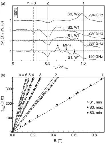
FIG. 1. (a) Cross section of the samples and the measurement circuitry. The lateral dimensions for sample S1 and S3 areL=3.4 mm anda=0.14 mm. The gate covers the whole width of the 2DES (W=1.5 mm). Sample S2 has only one ungated area with a= 0.3 mm, L=0.5 mm, andW=1 mm. The layer thicknesses as determined from the heterostucture growth ared1W1=142 nm,d1W2= 167 nm,d2W1=91 nm, andd2W2=85 nm.
were provided by modulation doping from a short-period GaAs/AlGaAs superlattice with a Si δ-doping layer located within the GaAs layers. This doping scheme [31,32] has been frequently used to enhance the fractional quantum Hall effect, but may also lead to a finite conductivity of the doping layer (DL) that survives down to the temperatures explored in the experiments here [33–35].
To measure the absorption of incident microwave radiation, we utilize a recently introduced bolometric method [33]. It is based on the extreme thermal sensitivity of the doping layer.
Its conductivity exhibits thermally activated behavior [33,35].
The measurement setup and a typical sample layout are illustrated in Fig.1. The absorption of microwave radiation by the highly conducting 2DES elevates the temperature of both the 2DES and the nearby DL. The microwave-induced heating is monitored by measuring the low-frequency impedance between the gate and alloyed contacts connected to both the 2DES and the DL. This impedance is very sensitive to changes in the DL conductivity at appropriately selected measurement frequencies (see Ref. [33] for details). In a current detecting scheme, an ac voltageVac,gwith an amplitude of 20 mV and a frequencyfbetween 5 and 60 Hz was applied to the gate. The generated ac-current signalIac,swas converted to an ac voltage Vac,s with the help of a transimpedance preamplifier whose output was measured with a dual-phase lock-in amplifier. In this work, we analyze the amplitude of the capacitive signal componentVc, i.e., the signal that is 90◦out-of-phase relative toVac,g. This capacitive signal always increases with increasing DL conductivity due to an absorption-induced temperature elevation [33]. Only a moderate radiation power Pmw has been used to ensure a linear relationship between Vc and the microwave absorption of the 2DES. The dc component of the gate voltage was kept zero for all data presented.
The samples were mounted in an oversized circular waveg- uide with a diameter of 18 mm and immersed in liquid3He in a cryostat with a temperature ofT =0.5 K. The normal to the 2DES was parallel to both the waveguide axis and a magnetic field B applied by a superconducting magnet. To
)0(V/)B(Vcc
0.0 0.2 0.4 0.6 0.8
0 100 200 300
(b) 1
S1, min S3, max S3, min 5 4 3
fwm)zHG(
B(T) 2 n= 6
0 0.5 1.0
1 1 1 1
S1, W1
337 GHz 237 GHz 294 GHz S3, W2
S2, W1
140 GHz MPR
(a)
S1, W1
fmw
2
c/
100%
1
3 2
n=
FIG. 2. (a) Microwave induced variation of the capacitive signal Vc,Vc(B), normalized to its zero magnetic field value, Vc(0), as a function of ωc/2πfmw. The data for three samples S1, S2, and S3 and different MW frequencies are shown. For the sake of clarity the curves are vertically shifted and the unity levels are marked by horizontal dashed lines. The abscissas were calculated for electrons with effective massmb=0.067me. Vertical solid lines mark positions of the cyclotron resonance and its second and third harmonics. The vertical dashed line corresponds to the position of the third harmonic assuming an electron effective massm∗=0.06me. On the lower curve the arrows mark the confined magnetoplasma resonances (MPRs). The wafer and sample numbers as well as the MW frequencies are listed for each curve. (b) Extrema in the bolometric response to microwave radiation (triangles - maxima, circles - minima) in the (B, fmw) plane. Open (closed) symbols have been used for sample S1 (S3). The dashed lines represent the magnetodispersion of the CR (n=1) and its second harmonic (n=2) for an electron effective massmb=0.067me. The solid lines mark CR harmonics withn=2,3,4,5,6 andm∗=0.06me.
irradiate the sample with microwave radiation backward-wave oscillators covering frequencies fmw between 10 GHz and 380 GHz were used. The maximum power level applied to the sample is estimated to be 1 mW. The magnetoresistance was measured on ungated samples processed from wafer W1.
Figure2(a)illustrates typical magnetic field dependencies of the bolometric response. Plotted is the microwave-induced change inVc, hereafter referred to asVc, for samples S1, S2 (both from wafer W1) and sample S3 (wafer W2). The results are presented with the ratioωc/2πfmwas the abscissa. Here,
ωc= |e|B/mbis the cyclotron frequency calculated using the valuemb=0.067mefor the electron effective mass. This ratio is proportional to the magnetic field B. The most striking features, present in all curves, are dips at the second and third CR harmonics. Note the large depth of these dips. It can exceed 50% of the photoresponse. This is the key experimental result. Weaker minima at higher harmonics are clearly seen on samples S1 and S2 and can also be resolved for sample S3. In our samples these minima in the magnetoabsorption become well pronounced at microwave frequencies above approximately 100 GHz and are dominant features above 200 GHz. Three additional peaks on the lower curve in between the CR and the second harmonic originate from the excitation of confined magnetoplasmons in the ungated part of sample S1. The complicated lateral sample geometry, formed by both gated and ungated areas, makes it necessary to distinguish signal contributions originating from these different parts of the sample. This can be accomplished by comparing the results measured at different frequenciesf[33,35]. Such comparison has shown that the features of the MW absorption at the CR harmonics described below are similar for gated and ungated parts of the sample, whereas the magnetoplasmon features stem from the ungated sample parts only. These plasmon modes are always present in the intermediate frequency range between 50 and 100 GHz and were reported earlier in Ref. [33].
For the sake of completeness, we mention a qualitative difference in the microwave photoresponse at the CR position (ωc/2πfmw=1) for samples produced from different wafers.
Whereas sample S3 shows a pronounced peak, the signals from samples S1 and S2 drop smoothly withωc/2πfmw. This different behavior is presently not understood.
The magnetic field locations of the CR peak (sample S3) and the dips at the CR harmonics (samples S1 and S3) have been collected in Fig.2(b)for the investigated frequency range. The CR peak and dip at the second harmonic follow straight lines corresponding to the electron effective massmb=0.067meof bulk GaAs. The other minima condense onto lines describing higher harmonics (2πfmw/ωc=n=3,4,5,6) for a different effective mass m∗=0.06me. The appearance of different effective masses is in accord with previous reports exploiting different transport phenomena to extract the mass. For instance, the effective mass obtained from the periodicity of the microwave-induced resistance oscillations (MIRO) is approximately 0.06me for our carrier densities [36–38]. A higher effective mass was obtained from the position of a narrow magnetoresistance spike at the second CR harmonic [22,39]. The values 0.066me[22] and 0.063me[39] have been reported.
In Fig. 3we present a comparison of the periodicity and phase of MIRO and our bolometrically detected absorption data in the magnetic field range corresponding to n2.
There is full correlation between these two signals. The positions of the magnetoabsorption minima coincide with nodes of MIRO. It is well established both theoretically and experimentally that these nodes occur at harmonics of the CR [13]. Hence, the data in Fig. 3 confirm that the minima in the magnetoabsorption trace indeed appear at the harmonics corresponding to effective massm∗=0.06me. Further elabo- rations on the different effective masses are relegated to future work.
fmw= 191 GHz (a)
0 0.1 0.2
0.0 0.5 1.0 (b)
B(T) )0(cV/)B(cV mwdP/ xxd
n=6 5 4 3 2
FIG. 3. Microwave photoresistancedρxx/dPmw (a) and magne- toabsorption signal (b) versus magnetic field for MW frequency fmw=191 GHz. The vertical dotted lines are drawn through the minima of the magnetoabsorption trace.
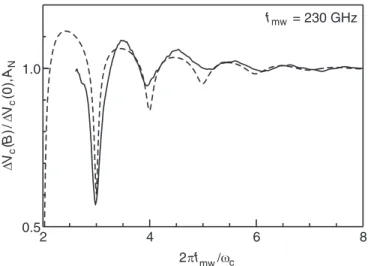
III. COMPARISON TO THEORY AND DISCUSSION In Fig.4we compare our main experimental findings with predictions of the theory of Ref. [30]. This theory accounts for memory effects in a 2DES subjected to disorder described by a two-component model including rare short-range scatterers
2 4 6 8
0.5 1.0
fmw= 230 GHz
2 fmw/ c
NccA),0(V/)B(V
FIG. 4. Experimental dependence Vc(B)/ Vc(0) versus 2πfmw/ωc calculated for m∗=0.06me (solid line) and its fit by ANgiven by Eqs. (1) and (2) (dashed line).fmw=230 GHz. The fit parameter values areτL=1.1 ns anda=24 nm.
(S) on top of a long-range smooth random potential (L). Within the Drude-Boltzmann description, these short- and long-range components of the random potential are characterized by their respective transport scattering ratesτS−1andτL−1. In the region
|ω±ωc| τ−1we are interested in (ω=2πfmw), the Drude absorptionADis proportional to the total transport rateτ−1= τS−1+τL−1. According to Ref. [30], inclusion of memory effects is equivalent to a replacement ofτS−1→(1−M)τS−1 in the Drude expression. The resulting absorption coefficient A, normalized to its Drude valueAD, is thus given by
AN≡A/AD =τ/τL+(1−M)τ/τS. (1) The non-Markovian correction M follows from the sum of probabilities to return to a strong impurity with cross section aafterncyclotron revolutions,
M=
∞
n=1
aδ−1
√π ncos2π nω ωc exp
−2π n
ωcτS −3π nω2 ω3cτL
. (2)
Hereδ=2vF
π/ωc3τL denotes the mean shift of the center of a cyclotron orbit over one cyclotron period due to angular diffusion in the smooth random potential andvF is the Fermi velocity. We note thatM(ωc=0)=0, so that normalization to the Drude absorption is equivalent to normalization to the zero magnetic field absorption. It is easy to see that memory effects induce 1/B-periodic oscillations in AN with minima at the CR harmonics. Moreover, these minima develop into sharp dips if the damping factor in the exponent of then=1 term is small, so that many terms contribute to the sum. Such dips can indeed be identified in the experiment when they are of intermediate amplitude. In the data presented here, this is mainly apparent for the absorption minimum at the third harmonic (see Figs.2–4). At fixed radiation frequencyfmw= ω/2π, the shape and low-B damping of magnetooscillations in Eq. (2) are fully determined by the values of τS andτL, while the cross sectiona enters as an overall prefactor. The shape and damping of the observed magnetooscillations can at all MW frequencies be fitted satisfactorily using a single value ofτL=1.1 ns. The other rateτS−1=τ−1−τL−1follows from the transport mobilityμ= |e|τ/mb. For example, for wafer W1,τ =0.27 ns and thereforeτS=0.36 ns. The validity of a single value forτLand the good agreement of the shape and relative depths of the dips forn3 supports the interpretation of the observed absorption minima in terms of memory effects [30]. The effective cross sectionafor short-range impurities, extracted from the fit to the data in Fig.4, equals 24 nm. This value is of the order of the Bohr radiusaB =10 nm as expected for background impurities sitting in the quantum well or close to the heterointerface. A comparison of the experimental data and theory for additional microwave frequencies is presented in AppendixA.
To further corroborate that memory effects are indeed important in our samples, we have measured the dc magnetore- sistanceρxx(see Fig.6in AppendixB). Similar to other recent reports [23–25,27], we observed a strong negative magnetore- sistance, which combines a parabolicT-independent region at lowB and a nonmonotonic T-dependent magnetoresistance at higherB. Note that the corresponding theory for parabolic magnetoresistance [10,11] employs the same two-component model of disorder and its result can be reproduced from Eq. (2)
by taking theω=0 limit. Comparison of the experimental magnetoresistance traces with predictions of Eq. (2) in this limit using the same parameter values as those used in Fig. 4 does reproduce the characteristic magnetoresistance value but does not yield the entire structure and temperature dependence. More systematic and complete studies of memory effects in magnetoresistance are still needed. In particular, one may expect electron-electron scattering to have an impact on these memory effects. It may also be responsible for the experimentally observed temperature dependence of the magnetoresistance.
For the sake of completeness, it should be mentioned that previous works on Si MOSFETs [40] and GaAs/AlGaAs het- erostructures [41] have also reported harmonic features in the MW absorption data. Unlike the present report, these studies revealedsmoothmagnetooscillations with absorptionmaxima at the CR harmonics. These oscillations were attributed to the effect of Landau quantization producing an ωc-periodic modulation in the energy dependence of the scattering rate and in the local density of states [42,43]. Here we report data at frequencies substantially larger than the maximum frequency addressed in Ref. [41] (fmw<60 GHz). At lower MW frequencies, our results indeed become more complex and maxima do occur at the CR harmonics whenfmw<50 GHz [35]. The mechanism for this transformation when moving to lower frequencies remains unclear.
IV. CONCLUSION
In summary, we have observed minima in the absorption of monochromatic microwave radiation by a 2DES at the har- monics of its cyclotron resonance frequency. This anomalous absorption behavior can be accounted for by non-Markovian electron dynamics, which allows for memory effects not captured in the Boltzmann kinetic theory. This explanation is also corroborated by the concomitant observation of negative magnetoresistance in the same material.
ACKNOWLEDGMENTS
We thank D. G. Polyakov for discussions. The experimen- tal investigations were supported by the Russian Scientific Foundation (Grant No. 14-12-00599, S.I.D. and A.A.K.).
I.A.D. gratefully acknowledges the support from the Deutsche Forschungsgemeinschaft (Project No. DM1/4-1). J.H.S. and V.U. acknowledge support from the GIF.
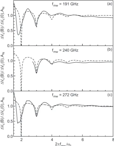
APPENDIX A: MAGNETOABSORPTION DATA FOR ADDITIONAL MICROWAVE FREQUENCIES The absorption curve shown in Fig.4 has been recorded at a microwave frequencyfmw=230 GHz. In this Appendix we present magnetoabsorption data (solid lines in Fig.5) for several additional microwave frequencies. The experimental data are compared with the theory reported in Ref. [30]
(dashed lines). Figures5(a)–5(c)correspond to illumination with fmw=191, 240, and 272 GHz microwave radiation.
Dashed lines in all panels represent the results of calculations using Eqs. (1) and (2). As in Fig. 4, the shape of the theoretical curves is determined by the single fit parameter
2 4 6 8 0.0
0.5 1.0
2 fmw/ c fmw= 272 GHz (c) 0.0
0.5 1.0
fmw= 191 GHz (a)
0.0 0.5 1.0
fmw= 240 GHz (b)
NccA),0(V/)B(VNccA),0(V/)B(VNccA),0(V/)B(V
FIG. 5. Magnetoabsorption data, Vc(B)/ Vc(0), plotted as a function of 2πfmw/ωc(solid lines). The abscissa has been calculated withm∗=0.06me. Fits to the experimental data withAN given by Eqs. (1) and (2) from the main text are included as dashed lines. All fits were obtained with a single value of the fit parameterτL=1.1 ns. (a), (b), and (c) correspond tofmw=191, 240, and 272 GHz. As for Fig.4, these data were obtained on sample S1.
τL=1.1 ns [andτS=(1/τ−1/τL)−1 0.36 ns follows from the transport mobilityμ= |e|τ/mb]. With the exception of the dip at the second CR harmonic 2πfmw/ωc=n=2, theory reproduces the shape and relative magnitude of the dips in the magnetoabsorption data quite well for all frequencies.
The above mentioned discrepancy between the data and theory near the second CR harmonic should not be considered as a failure of the proposed explanation since Eq. (2) is derived assuming|M| 1 while the observed dip atn=2 corresponds to|M| ∼1 [44]. When the probability of return to a short-range impurity becomes sufficiently large, processes with multiple returns should be taken into account self- consistently. Such self-consistent calculations are expected to reduce the magnitude and broaden the width of the largest dips, in accordance with the data in Fig.5. The origin of the shift in position of the experimental dip at the second CR harmonic relative to the 2πfmw/ωc=2 value, which has been discussed in the main text in terms of a different effective mass, remains unclear.
In Eqs. (1) and (2), the magnitude of the memory effect is proportional to the cross sectiona of a short-range impurity.
These impurities are treated as identical classical hard-wall scatterers. Matching the magnitude of the dips for the data
2 . 0 0
. 0 2
. 0 - -0.4 -0.2 0.0
B (T)
T=0.5 K -9B2
-180B2
-16B2 -230 B2
T=1.5 K 1)0(/)B(xxxx
FIG. 6. Solid lines: normalized longitudinal dc resistance ρxx(B)/ρxx(0)−1 as a function of B, measured on a Hall bar sample processed from wafer W1. The data has been recorded at T =0.5 K and T =1.5 K as marked. Dotted and dashed lines:
parabolic fitsρxx(B)/ρ(0)−1= −cB2+C0 to magnetoresistance in regions of weak (dotted lines,C0=0) and moderateB(dashed lines,C0≈ −0.07). The parabolic dependence−cB2with numerical value of the fit parametercin units of T−2is provided for every line.
shown in Fig. 5 using Eqs. (1) and (2) yields the effective cross sectiona=37, 22, and 14 nm forfmw=191, 240, and 272 GHz, respectively. These values are in the expected range a∼aB for background impurities present in the immediate vicinity of the 2DES. Here aB 10 nm is the Bohr radius characterizing the spatial scale below which static screening of the impurity potential by the 2DES becomes ineffective.
The variation of a(fmw) should not be taken literally as a dependence of the cross section for short-range impurity scattering on magnetic field or microwave frequency. It rather signals that while the model of Ref. [30] captures the essential physics, it is insufficient to reproduce all quantitative features of the experimental data. Hence, it is desirable to study analytically and simulate numerically the electron dynamics using more elaborate models. In addition, the influence of electron-electron interactions on the memory effects deserves attention.
APPENDIX B: NEGATIVE MAGNETORESISTANCE IN THE DC TRANSPORT
In Fig.6we present the magnetoresistanceρxx(B) normal- ized to its value ρxx(0) at B=0 recorded at two different temperatures on an ungated sample produced from wafer W1. The experimental traces exhibit two distinct negative magnetoresistance contributions that can be clearly separated.
The first contribution is restricted to a narrow region around B=0 and only exhibits a weak T dependence, while the second contribution extends up to much higher B field and possesses an apparentT dependence as well as a quadraticB dependence at moderate magnetic fields. These observations are similar to results reported in Refs. [22–27]. To quantify the observed behavior, we fit both the narrow and wide magnetoresistance contributions with parabolas according to ρxx(B)/ρ(0)−1= −cB2+C0. These parabolic fits have
been added as dotted (C0=0) and dashed (C0≈ −0.07) lines in Fig.6. The extracted curvature coefficientscin units of T−2 have been included in Fig.6.
The narrow magnetoresistance peaks have been previously attributed to non-Markovian memory effects [27]. They ap- parently result from so-called oval defects, which have large sizea aB and originate from Ga droplets that form during the growth process [27]. The corresponding theory for the parabolic magnetoresistance [10,11,27] considers the same two-component model of disorder as Ref. [30]. The expected dc magnetoresistance can be calculated from Eq. (2) in the ω=0 limit,
ρxx(B)
ρxx(0) −1= −aδ−1 1+τS/τL
∞
n=1
√1 π nexp
−2π n ωcτS
. (B1)
Both the narrow as well as wide parabolic features in the magnetoresistance mostly belong to the range of classically strong magnetic fields,ωcτ 1 (ωcτ ∼1 corresponds toB∼ 1 mT). For parameters used in Fig. 5 and Fig.4, τ ∼τS∼ 0.3τL,ωcτS1 and Eq. (B1) can be approximated as
ρxx(B)/ρxx(0)−1= −ω2c/ω20, (B2) where ω−02 av−F1
τSτL/8π2(1+τS/τL)−1, in accord with the result of Ref. [10].
With the parameters used in Figs. 4 and 5 together with the density and mobility for sample S1, we obtain ρxx(B)/ρxx(0)−1= −cB2 from Eq. (B2) with c[T−2] 1.7a[nm], where expressions in square brackets denote the units for the corresponding quantities. Within the interpre- tation of Ref. [27], this yields an effective cross section for scattering off of oval defects of the order of 0.1 μm. The same procedure for the wide parabolic magnetoresistance contribution yields a 9 nm at T =0.5 K and a 5 nm at T =1.5 K. These cross sections are likely associated with charged impurities in the close vicinity of the 2DES, the second source of short-range scattering. These cross- section values are similar to the values extracted from the magnetoabsorption data. This points to a common origin of the wide negative magnetoresistance contribution and the dips in the magnetoabsorption and corroborates the importance of memory effects. The temperature dependence remains an unresolved discrepancy between experiment and theory [45].
We speculate that the temperature dependence can originate from the influence of electron-electron interactions which should enhance the probability to miss the strong impurity after one or more cyclotron revolutions. This mechanism does not violate Kohn’s theorem and should lead to a reduction of the memory effect with increasing T similar to what is observed here in experiment.
[1] A. D. Mirlin, J. Wilke, F. Evers, D. G. Polyakov, and P. Wölfle, Strong Magnetoresistance Induced by Long-Range Disorder, Phys. Rev. Lett.83,2801(1999).
[2] E. M. Baskin, L. N. Magarill, and M. V. Entin, Two-dimensional electron-impurity system in a strong magnetic field, Zh. Eksp.
Teor. Fiz.75, 723 (1978) [Sov. Phys. JETP48, 365 (1978)].
[3] E. M. Baskin and M. V. Entin, Magnetic localization of classical electrons in 2D disordered lattice,Physica B249,805(1998).
[4] A. V. Bobylev, F. A. Maao, A. Hansen, and E. H. Hauge, Two-Dimensional Magnetotransport According to the Classical Lorentz Model,Phys. Rev. Lett.75,197(1995).
[5] A. V. Bobylev, F. A. Maao, A. Hansen, and E. H. Hauge, There is more to be learned from the Lorentz model,J. Stat. Phys.87, 1205(1997).
[6] A. Kuzmany and H. Spohn, Magnetotransport in the two- dimensional Lorentz gas,Phys. Rev. E57,5544(1998).
[7] A. Dmitriev, M. Dyakonov, and R. Jullien, Classical mechanism for negative magnetoresistance in two dimensions,Phys. Rev. B 64,233321(2001).
[8] V. V. Cheianov, A. P. Dmitriev, and V. Yu. Kachorovskii, Non- Markovian effects on the two-dimensional magnetotransport:
Low-field anomaly in magnetoresistance, Phys. Rev. B 70, 245307(2004).
[9] M. M. Fogler, A. Yu. Dobin, V. I. Perel, and B. I. Shklovskii, Suppression of chaotic dynamics and localization of two- dimensional electrons by a weak magnetic field,Phys. Rev. B 56,6823(1997).
[10] A. D. Mirlin, D. G. Polyakov, F. Evers, and P. Wölfle, Quasiclassical Negative Magnetoresistance of a 2D Electron gas: Interplay of Strong Scatterers and Smooth Disorder, Phys. Rev. Lett.87,126805(2001).
[11] D. G. Polyakov, F. Evers, A. D. Mirlin, and P. Wölfle, Quasiclassical magnetotransport in a random array of antidots, Phys. Rev. B64,205306(2001).
[12] I. A. Dmitriev, F. Evers, I. V. Gornyi, A. D. Mirlin, D. G. Polyakov, and P. Wölfle, Magnetotransport of electrons in quantum Hall systems, Phys. Status Solidi B 245, 239 (2008).
[13] I. A. Dmitriev, A. D. Mirlin, D. G. Polyakov, and M. A. Zudov, Nonequilibrium phenomena in high Landau levels,Rev. Mod.
Phys.84,1709(2012).
[14] F. Evers, A. D. Mirlin, D. G. Polyakov, and P. Wölfle, Semiclassical theory of transport in a random magnetic field, Phys. Rev. B60,8951(1999).
[15] J. H. Smet, Ballisic transport of composite fermions in semi- conductor nanostructures, inComposite Fermions, edited by O.
Heinonen (World Scientific, Singapore, 1998).
[16] G. M. Gusev, P. Basmaji, Z. D. Kvon, L. V. Litvin, Yu. V. Nastau- shev, and A. I. Toropov, Negative differential magnetoresistance and commensurability oscillations of two-dimensional electrons in a disordered array of antidots,J. Phys.: Condens. Matter6, 73(1994).
[17] K. Tsukagoshi, S. Wakayama, K. Oto, S. Takaoka, K. Murase, and K. Gamo, Magnetotransport through disordered and anisotropic antidot lattices in GaAs/AlxGa1−xAs heterostruc- tures,Phys. Rev. B52,8344(1995).
[18] G. Lütjering, Nanostrukturierte Antidot-Systeme, Ph. D. thesis, Stuttgart University, 1996.
[19] G. Nachtwei, Z. H. Liu, G. Lütjering, R. R. Gerhardts, D. Weiss, K. von Klitzing, and K. Eberl, Critical currents in quantum Hall conductors with antidot arrays, Phys. Rev. B 57, 9937 (1998).
[20] S. Cina, D. D. Arnone, H. P. Hughes, C. L. Foden, D. M.
Whittaker, M. Pepper, and D. A. Ritchie, Electron dynamics of a two-dimensional electron gas with a random array of InAs quantum dots,Phys. Rev. B60,7780(1999).
[21] O. Yevtushenko, G. Lütjering, D. Weiss, and K. Richter, Weak Localization in Antidot Arrays: Signature of Classical Chaos, Phys. Rev. Lett.84,542(2000).
[22] Y. Dai, R. R. Du, L. N. Pfeiffer, and K. W. West, Observation of A Cyclotron Harmonic Spike in Microwave-Induced Resistances in Ultraclean GaAs/AlGaAs Quantum Wells,Phys. Rev. Lett.
105,246802(2010).
[23] L. Bockhorn, P. Barthold, D. Schuh, W. Wegscheider, and R. J. Haug, Magnetoresistance in a high-mobility two- dimensional electron gas,Phys. Rev. B83,113301(2011).
[24] A. T. Hatke, M. A. Zudov, J. L. Reno, L. N. Pfeiffer, and K. W. West, Giant negative magnetoresistance in high-mobility two-dimensional electron systems,Phys. Rev. B85,081304(R) (2012).
[25] R. G. Mani, A. Kriisa, and W. Wegscheider, Size-dependent giant-magnetoresistance in millimeter scale GaAs/AlGaAs 2D electron devices,Sci. Rep.3,2747(2013).
[26] Q. Shi, P. D. Martin, Q. A. Ebner, M. A. Zudov, L. N. Pfeiffer, and K. W. West, Colossal negative magnetoresistance in a two-dimensional electron gas, Phys. Rev. B 89, 201301(R) (2014).
[27] L. Bockhorn, I. V. Gornyi, D. Schuh, C. Reichl, W. Wegscheider, and R. J. Haug, Magnetoresistance induced by rare strong scatterers in a high-mobility two-dimensional electron gas, Phys. Rev. B90,165434(2014).
[28] P. S. Alekseev, Negative Magnetoresistance in Viscous Flow of Two-Dimensional Electrons,Phys. Rev. Lett.117,166601 (2016).
[29] D. G. Polyakov, F. Evers, and I. V. Gornyi, Cyclotron resonance in antidot arrays, Phys. Rev. B 65, 125326 (2002).
[30] I. A. Dmitriev, A. D. Mirlin, and D. G. Polyakov, Oscillatory ac conductivity and photoconductivity of a two-dimensional electron gas: Quasiclassical transport beyond the Boltzmann equation,Phys. Rev. B70,165305(2004).
[31] K.-J. Friedland, R. Hey, H. Kostial, R. Klann, and K. Ploog, New Concept for The Reduction of Impurity Scattering in Remotely Doped GaAs Quantum Wells, Phys. Rev. Lett. 77, 4616 (1996).
[32] V. Umansky, M. Heiblum, Y. Levinson, J. Smet, J. Nübler, and M. Dolev, MBE growth of ultra-low disorder 2DEG with mobility exceeding 35×106cm2/Vs, J. Cryst. Growth 311, 1658(2009).
[33] S. I. Dorozhkin, D. V. Sychev, and A. A. Kapustin, Bolometric detection of magnetoplasma resonances in microwave absorp- tion by two-dimensional electron systems based on doping layer conductivity measurements in GaAs/AlGaAs heterostructures, J. Appl. Phys.116,203702(2014).
[34] S. Peters, L. Tiemann, C. Reichl, S. Fält, W. Dietsche, and W.
Wegscheider, Improvement of the transport properties of a high- mobility electron system by intentional parallel conduction, Appl. Phys. Lett.110,042106(2017).
[35] S. I. Dorozhkin and A. A. Kapustin, Features of microwave ab- sorption by two-dimensional electron systems at the harmonics of cyclotron resonance, Pis’ma Zh. Eksp. Teor. Fiz.101, 101 (2015) [JETP Lett.101,97(2015)].
[36] A. T. Hatke, M. A. Zudov, J. D. Watson, M. J. Manfra, L. N.
Pfeiffer, and K. W. West, Evidence for effective mass reduction in GaAs/AlGaAs quantum wells,Phys. Rev. B87,161307(R) (2013).
[37] A. V. Shchepetilnikov, D. D. Frolov, Yu. A. Nefyodov, I. V.
Kukushkin, and S. Schmult, Renormalization of the effective mass deduced from the period of microwave-induced resistance oscillations in GaAs/AlGaAs heterostructures,Phys. Rev. B95, 161305(R)(2017).
[38] X. Fu, Q. A. Ebner, Q. Shi, M. A. Zudov, Q. Qian, J. D. Watson, and M. J. Manfra, Microwave-induced resistance oscillations in a back-gated GaAs quantum well,Phys. Rev. B95,235415 (2017).
[39] A. T. Hatke, M. A. Zudov Pfeiffer, and K. W. West, Giant microwave photoresistivity in high-mobility quantum Hall systems,Phys. Rev. B83,121301(R)(2011).
[40] G. Abstreiter, J. P. Kotthaus, and J. F. Koch, Cyclotron resonance of electrons in surface space-charge layers on silicon,Phys. Rev.
B14,2480(1976).
[41] O. M. Fedorych, M. Potemski, S. A. Studenikin, J. A. Gupta, Z. R. Wasilewski, and I. A. Dmitriev, Quantum oscillations in the microwave magnetoabsorption of a two-dimensional electron gas,Phys. Rev. B81,201302(R)(2010).
[42] T. Ando, Theory of cyclotron resonance lineshape in a two- dimensional electron system, J. Phys. Soc. Jpn. 38, 989 (1975).
[43] I. A. Dmitriev, A. D. Mirlin, and D. G. Polyakov, Cyclotron- Resonance Harmonics in The ac Response of a 2D Electron Gas with Smooth Disorder,Phys. Rev. Lett.91,226802(2003).
[44] Full analysis was so far performed [29] only for a random antidot array without smooth disorder.
[45] An alternative explanation [28] of the wideT-dependent peak is based on effects of viscous flow of electron liquid between the oval defects.