Analysis of the charge collection process in pnCCDs
N. Kimmel
a,d, R. Hartmann
c,d, P. Holl
c,d, N. Meidinger
a,d, R. Richter
b,d, L. Str¨ uder
a,da
Max-Planck-Institut f¨ ur extraterrestrische Physik, Giessenbachstraße, 85748 Garching, Germany;
b
Max-Planck-Institut f¨ ur Physik, F¨ ohringer Ring 6, 80805 M¨ unchen, Germany;
c
PNSensor GmbH, R¨ omerstraße 28, 80803 M¨ unchen, Germany;
d
MPI Halbleiterlabor, Otto-Hahn-Ring 6, 81739 M¨ unchen Germany;
ABSTRACT
At MPI Halbleiterlabor, pnCCDs have been continuously developed to improve readout noise, readout speed, charge transfer efficiency and energy resolution. Pixel sizes of 75µm, 51µm and 36µm were realized in addition to the original 150µm pixel design. Reduction of the pixel size evidently changes the electric fields in the pixel structure. This leads to the question of how scaling of the pixel size affects the charge collection at subpixel dimensions. We used the ”mesh-method” to measure the amount of signal charge deposited in a pixel depending on the position of X-Ray photon incidence within the pixel. In this experiment, a mesh with a rectangular hole pattern was mounted above the entrance window or structured front side of the detector. A slight rotation of the mesh ensures that every hole has a different position relative to the pixel below. It corresponds to scanning of a single pixel. Measurements were done with pnCCDs of 150µm, 75µm and 51µm pixel size at photon energies from 0.7keV to 5.4keV. We also used a setup with front side illumination of a pnCCD with 75µm pixel size to investigate the absorption of X-ray photons in the register structure of the device. Numerical simulations delivered results for signal charge distribution into pixels along the charge transfer direction. We analyzed the charge collection in a pixel and the absorption properties of the register structure with a spatial resolution below 5µm and could investigate the accuracy of numerical device simulations.
Keywords: pnCCD, X-Ray, X-Ray detectors, device analysis, charge collection, mesh method
1. INTRODUCTION
The mesh experiment has been introduced as a method for the analysis of pixelized detectors by Tsunemi et al. .1 It was shown that properties like the charge collection behaviour2 3 and the sensitivity to photons in a pixel4can be analyzed to a resolution in the micrometer range. We have adapted this method to the pnCCDs produced in our lab and developed our own analysis procedure for data obtained with mesh measurements. In addition we used a numerical device simulation software to simulate the charge collection process in the used pnCCD with 75µm pixel size and 280µm thickness of the fully depleted5 silicon substrate. A comparison of simulations and measurements helps to verify that our physical model of this pnCCD conforms with the real device. A drawing of the setup principle is shown in fig. 1.
2. MEASUREMENT SETUP
For all measurements we employed meshes of the same geometry and material. The meshes consist of a 10µm thick gold foil and have holes of 5µm diameter arranged in a rectangular array with 150µm hole distance. See fig. 2 for a view of the mesh mounted on a 150µm pixel XMM-type pnCCD. An area of maximally 11x16mm2is covered where the width of the covered sensitive area of the used devices is 9.6mm (150µm and 75µm pixels) and 13.1mm (51µm pixels). This amounts to at least 4000 holes lying in the sensitive area and thus 4000 different hole positions relative to the pixel below. For mechanical stability, the gold mesh was mounted in a steel frame
Further author information: (Send correspondence to N. Kimmel)
N. Kimmel: E-mail: nik@hll.mpg.de, Telephone: +49 89 83940017, Fax: +49 89 83940013
pnCCD type pixel size temperature back contact registers
V9 XMM-type 150x150µm2 125K -170V -15V Phi2/3 storage -20V Phi1 barrier V10 framestore #1 75x75µm2 193K and 153K -90V -15V Phi2/3 storage -21V Phi1 barrier V10 framestore #2 75x75µm2 153K -90V -17V Phi2/3 storage -25V Phi1 barrier V11 framestore 51x51µm2 180K -250V -15V Phi2/3 storage -19V Phi1 barrier
Table 1.Operating voltages and temperatures of the devices during measurements. The optimal voltages depend on the design of the device and can not be freely set for a comparison of pixel geometries. Low temperatures were chosen to supress any dark current contribution during integration times of 0.2s to 0.36s.
pnCCD type pixel size geometry substrate thickness illumination
V9 XMM-type 150x150µm2 64 channels, 200 rows 290µm back side V10 framestore #1 75x75µm2 128 channels, 125 rows imaging area 280µm back side V10 framestore #2 75x75µm2 128 channels, 125 rows imaging area 280µm front side V11 framestore 51x51µm2 264 channels, 264 rows imaging area 450µm back side
Table 2. Geometrical parameters of the pnCCDs used for mesh measurements. The V9 to V11 designation gives the production generation of the device. Devices of version V9 and V10 are made on 4 inch wafers; V10 with 280µm thickness, V9 devices are made on wafers with an additional epi layer and 290µm thickness. The devices from production V11 came available in 2005 and are made on 6 inch wafers of 450µm thickness.
which was mounted either directly on the ceramic board carrying the pnCCD or on the cooling mask of the setup. In either case the distance mesh to pnCCD was smaller than 4mm. Mesh and pnCCD were mounted in an X-ray facility with a distance of 4m to the X-ray source. We used varoius anode targets for X-ray photon energies of 277eV (C-Kα), 705eV (Fe-Lα), 930eV (Cu-Lα), 1487eV (Al-Kα), 1774eV (W-Mα), 4510eV (Ti-Kα) and 5415eV (Cr-Kα). The photon rate was adjusted to 50-100 photons per frame. With the attenuation factor of 8.73·10−4of the mesh in combination with the maximum flux of the X-ray tube, an integration time of 200ms to 360ms was needed. In order to supress any possible noise contribution by thermal dark current, we cooled the devices to -148(150µm pixel pnCCD6), -120(75µm pixel pnCCD7 with front- and back side illumination), -90(51µm pixel pnCCD8 9) and -80 (75µm pnCCD with backside illumination).
3. DATA ANALYSIS METHOD
For each mesh measurement, we took four different data sets: 200 dark frames before a calibration measurement of 5000 frames with flat field illumination and 200 dark frames before a measurement of 10000 frames with illumination through the mesh. Both with flat field illumination and illumination through the mesh, the same X-ray photon energy is used. Dark frames are used to determine noise and pedestal for each pixel. For signal frames, the constant offset is substracted from the pixel signal and the noise is used to define the threshold above which a signal is detected as a photon hit. In the used pnCCDs with full depletion of the detection volume, the high drift field allows for charge spreading over up to four pixels. For a valid photon pattern, all pixels with a signal above the threshold must lie in a square of 2x2 pixels.
3.1. Calibration
All signals above the noise threshold are selected from flat field calibration frames and if possible recombined to patterns with their neighbors. With the measured pulse height of a pattern and the given peak energy of the used X-ray line, charge transfer efficiency and gain are determined for each channel. Gain and charge transfer efficiency of a flat field measurement are then used for calibration of the appropriate mesh measurement.
3.2. Pixel reconstruction
If all photon event patterns collected for a mesh measurement are displayed in a single frame image, one can see the pixels illuminated by a hole as bright spots. If only patterns consisting of a single pixel are shown, a moir´e pattern occurs which consists of pixels where these patterns appear. A similar moir´e pattern occurs if only patterns are shown where the sum of the pulse heights is dominated by the contribution of one pixel.
Figure 1.Principle of the mesh setup, this drawing equivalents to a setup where the hole distance is equal to the pixel size. If only single events are shown in a frame, dark moir´e lines occur where hole lines cross pixel borders with a small ≈4°angle. Horizontal and vertical holes lines and pixel borders can be treated independently in a mesh position analysis.
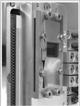
Figure 2.Gold mesh with holder mounted on the cooling mask of a 75µm pixel pnCCD test setup. All areas except the mesh are shielded from X-rays with 0.5mm copper sheet. The mesh is not visible here as its mount extrudes into the cooling mask.
Offset to the lower left frame corner, distance and angle of the dark moir´e lines define the location of the mesh holes relative to the pnCCD pixels. We have developed and implemented an analysis method to determine the parameters of the moir´e line system and to derive the positions of the mesh holes from them. If all hole positions are known, the response of a pixel to the photon incidence position can be reconstructed from the data. For our analysis, we generated six different types of maps of a pixel: I. A map showing the average number of photons counted at a given hole position II. four maps showing the occurence of single, double, triple and quadruple split events in a pixel. Split events with more than four split partners were not observed with the used pnCCDs.
III. a map of the charge collection function showing the relative amount of photon generated charge collected in a pixel depending on the photon incidence position. For all of these maps, only photons in an energy range centered on the used X-ray line are selected.
4. RESULTS OF DATA ANALYSIS
Pixel maps showing the occurence of a certain (split-) event type are not used by us for a quantitative analysis but are important for checking qualitative results expected from a physical model of a pnCCD. They also show if the mesh position was determined correctly. In figures 3, 4, 5 and 6 the occurence of split events is shown for a 75µm pixel framestore pnCCD illuminated through the entrance window on its back side.
As expected, single events occur if photons hit the middle of a pixel while quadruple split events occur if photons hit the corner of a pixel. Triple splits also occur near a corner but not directly on it, double splits occur near the pixel border where signal charge does not reach a third or fourth pixel. If the region where single events occur was shifted relative to the middle of the pixel map, this would indicate that the mesh position was not determined correctly. We generated split event maps for all data sets and checked if the mesh position reconstruction was done correctly as well as our expectations for the split event locations.
Figure 3. Single events gen- erated by 4510eV Ti-Kαpho- tons in a 3x3 pixel map.
Charge transfer is from top to down. The channel coor- dinate is increasing from left to right.
Figure 4. Same as in fig.
3, but double split events are shown. A pixelmap is tiled to a 3x3 map for better illus- tration of the response at the pixel borders.
Figure 5. Same as in fig. 3, but with triple events. Grey shades indicate that there are transition regions where triple events occur with a certain probability.
Figure 6. Same as in fig.
3, but for quadruple events.
They are exactly centered on the pixel corners.
4.1. Influence of the pixel size
Maps of the charge collection function reflect the influence of the signal charge cloud size after drift through the depleted volume and before separation into one or more pixels. The form of this function can be described as an error function. With a least squares fit of an error funtion, the sigma of the charge cloud as a gaussian can be found. This sigma mainly depends on the drift distance before separation of the charge cloud and the back contact voltage. For a known photon energy, the drift distance cannot be varied and has a mean value given by the detector thickness minus the absortion depth below the entrance window and the separation depth below the front side. In our case, the separation depth is an unknown parameter and is best determined from simulations after their verification with measurement data.
Figure 7. Charge collection function of a 150x150µm2 pixel pnCCD, the mean charge cloud size is 6.54µm.
Figure 8. Charge collection function of a 75x75µm2 pixel pnCCD with a mean charge cloud size of 7.02µm.
Figure 9. Charge collection function of a 51x51µm2 pixel pnCCD, we mea- sured a mean charge cloud size of 9.07µm.
Figures 7, 8 and 9 have a scale normalized to the pixel size and show an area of 3x3 pixels of the charge collection function measured with the Ti-Kαline (4510eV). It is easy to see that for smaller pixel sizes charge is spreaded over a larger area relative to the pixel size. With the 51µm pixel pnCCD there is the additional effect of a larger thickness of 450µm of the device, see table 2. The results for the measured charge cloud size are: 6.7µm (row) 6.38µm (transfer) for the 150x150µm2 pixel pnCCD, 7.12µm (row) 6.91µm (transfer) for the 75x75µm2 pixel pnCCD and 9.27µm (row) 8.88µm (transfer) for the 51x51µm2 pixel pnCCD. All measurements were done with the same X-ray energy of 4510eV; the temperature was not equal: 125K with 150µm pixels, 193K with 75µm pixels and 183K with 51µm pixels. As a first conclusion we can say that the measured effective charge
cloud size mainly depends on the drift distance i.e. the thickness of the device and to a much lesser extend on the pixel size. It must also depend on the back contact voltage as it influences the drift time and thus the time for expansion of the charge cloud due to diffusion and electrostatic repulsion. A measurement with the 75x75µm2 pixel pnCCD at 153K and the same energy confirms that the operating temperature has a rather small influence.
4.2. Energy dependence
Figure 10.Projection of the charge collection function of a 75x75µm2 pixel pnCCD along the transfer direction at 1774eV,σtransfer= 6.51µm and 4510eV,σtransfer= 6.91µm.
Figure 11.Projection of the charge collection function of a 51x51µm2 pixel pnCCD along the transfer direction at 1774eV,σtransfer= 8.61µm and 4510eV,σtransfer= 8.88µm.
A variation of the X-ray photon energy has three possible influences on the analysis results. I. If the signal threshold is constant, split partners that are smaller relative to the total signal amplitude can still be detected at higher energies. II. At higher photon energies, the number of signal electrons is proportionally higher. Above a certain number of generated charges, electrostatic repulsion significantly increases the size of the charge cloud;
the holes also generated by photon absorption are immediately separated from the electrons in the drift field and have no significant effect. III. Depending on the mean penetration depth, the drift distance and therefore the drift time before separation varies and influences the measured size of the charge cloud. Only effects II. and III.
are of physical origin, effect I. is an analysis artefact to be considered for the analysis of pixel maps. We chose the characteristic X-ray lines of W-M (1774eV) and Ti-Kα(4510eV) for measurements as their mean penetration depth in silicon is nearly equal: 12.5µm (W-M) and 13.0µm (Ti-Kα). The measured difference of the charge cloud size must then be the result of electrostatic repulsion because diffusion of a charge cloud does not depend on the number of charge carriers. Figures 10 and 11 show that the effect is very small. It only appears in a numerical analysis of the data with a least squares fit to the charge collection function that delivers the sigma of a gaussian charge cloudσcharge cloudfor row and transfer directionσrow,σtransfer. For the 75x75µm2pixel pnCCD we obtain charge cloud sizes of 6.70µm (row) 6.51µm (transfer) at 1774eV and 7.12µm (row) 6.91µm (transfer) at 4510eV. For the 51x51µm2pixel pnCCD we obtain values of 9.02µm (row) 8.61µm (transfer) at 1774eV and 9.27µm (row) 8.88µm (transfer) at 4510eV. The mean differences are 0.25µm for 51µm pixel size and 0.4µm for 75µm pixel size, a value at the limit of our measurement accuracy.
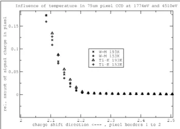
4.3. Temperature effects
Charge carrier mobility and also the diffusion constant both depend on temperature. As a net effect for lower temperatures, the charge cloud size is smaller after a given drift distance if all other operating parameters of a pnCCD remain unchanged. Our measurements with the 75µm pixel pnCCD show a very small effect, see figures 12 and 13. A quantitative analysis was done by a least squares fit of the data to an error function both in charge transfer and line direction. We obtained charge cloud sizes of 7.12µm and 7.02µm (row at 193K and 153K) and 6.91µm and 6.78µm (channel at 193K and 153K) with the 4510eV Ti-Kαline. This is a mean difference of 0.12µm or 1.7%. For the 1774eV W-M line we obtained 6.70µm and 6.58µm (row at 193K and 153K) and
Figure 12.Projection of the charge collection function of a 75x75µm2 pixel pnCCD along the transfer direction at 1774eV (W-M) for device temperatures of 153K and 193K.
Figure 13. Projection of the charge collection function of a 75x75µm2 pixel pnCCD along the transfer direction at 4510eV (Ti-Kα) for device temperatures of 153K and 193K.
6.51µm and 6.38µm (channel at 193K and 153K) corresponding to a mean difference of 0.13µm or 1.9%. If we only look at diffusion related expansion of an electron cloud, the sigma of a gaussian after timet is:
σn= r
2· k·T
e ·µn·t (1)
withkbeing the Boltzmann constant,µnthe electron mobility,ethe elementary charge andσnthe sigma of the electron cloud. For a shallow doped and overdepleted device, t is inversely proportional toµn and the ratio of σnvalues for two temperatures is given byp
T1/T2. In our case we compared measurements at 153K and 193K resulting in a ratio of p
193/153 = 1.12, a difference of 12%. A comparison with the results of the fit to the charge collection function shows that the theoretical value is 7 times higher than the measured value! At this point we are obviously at the limits of measurement accuracy and a close inspection of the reconstructed pixel images shows an irregular warping of the mesh which is cooled with the device. An irregular error of the mesh hole positions which are assumed to be on a regular grid causes a smearing of the charge collection function which explains a measured charge cloudσwhich is too large for low temperatures.
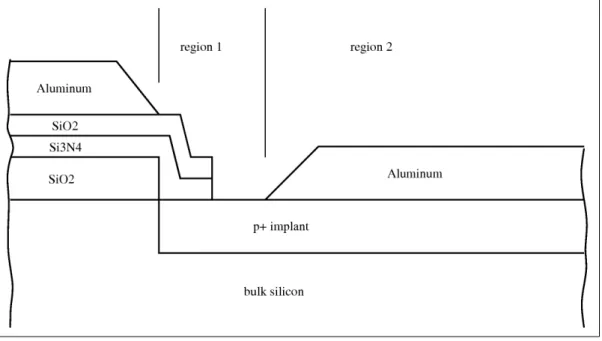
4.4. Photon absorption in the register structure
If a pnCCD is illuminated from the front side which carries the register structure, photons have to pass through the layers of this structure, compare figure 14. With the mesh experiment in combination with front side illumination, we studied the absorption of photons in the various oxide, nitride and aluminum layers of the front side structure. While we could not measure the absolute flux, it is possible to compare the number of counted photons for different hole positions. In combination with our complete knowledge of the production process, it is possible to calculate the expected ratio of the photon count number for different regions in the pixel. If the hole size is considered together with the structure size, it turns out that only the aluminum contact of the p+
register corresponding to region 2 shown in fig. 14 is much lager than a hole. As shown in fig. 14 in region 1, a hole always covers more than one layer and the number of counted photons is determined by the mean absorption of all covered layers. In the figures shown in 15, the qualitative expectations for the experiment are confirmed: The absorption of photons is high in the aluminum register contact and in the MOS-Gate aluminum contact and oxide layers but low in the regions with open Silicon. We also see a strong contrast between Al-Kα and W-M as the W-M line has an energy above the K-edge of aluminum and is thus strongly absorbed. A detailed analysis was done for the region of the p+ register implant which is partly covered by an aluminum contact, partly open silicon and partly covered by a combination of Silicon nitride and Silicon oxide layers. For low energies, the maximum photon count must occur in region 1 of fig. 14 with open silicon and silicon covered
Figure 14. Cut through a part of the channel region of a 75µm pixel pnCCD. For a first analysis of data with front side illumination, we calculated the flux for hole positions above region 1 and above region 2. The diameter of the hole is nearly equal to the width of region 1. Absorption in region 1 is thus the mean absorption of the area below the hole while the absorption in region 2 is defined by the thickness of the aluminum layer.
by nitride and oxide. For a comparison with the measured count rate, we calculated the absorption in region 1 and region 2. Absorption in the p+ doped area below was assumed to be constant for both regions. We see a good confirmation of our model for low energies and corresponding high contrast. Despite good contrast caused by strong absorption in the aluminum contact, the value for the W-M line has a rather high error. A variation of the assumed layer thickness of aluminum results in bigger errors of the results for Fe-L and Cu-L. The strong absorption at the MOS-gates even for the Al-Kα and Ti-Kαlines with high penetration depths in aluminum indicates that there must be an insensitive layer not only of aluminum and oxides/nitrides but also of bulk silicon from where signal electrons are not collected in the pixel. For the Cr-Kαmeasurement, the count rate map of the pixel is nearly flat.
X-ray line theoretical measured error X-ray line theoretical measured error
Fe-L 705eV 1.791 1.794 0.4% Cu-L 930eV 1.299 1.2885 3.5%
Al-Kα1487eV 1.0725 1.0638 12% W-M 1775eV 2.230 1.920 25%
Ti-Kα4510eV 1.061 1.026 57% Cr-Kα5415eV 1.036 ≈1 –
Table 3. Expected and measured photon count ratios calculated as (counts in region 1)/(counts in region 2), compare fig. 14. For Cr-Kα, the ratio cannot be measured as nearly all photons pass through aluminum and oxide+nitride layers.
We are interested in the difference of the ratio to 1. Therefore the error increases drastically as the ratio gets close to 1 for higher energies.
5. DEVICE SIMULATIONS
Device simulations were set up with the two dimensional device simulation program ’TeSCA’. We simulated a cut through the middle of a channel along the charge transfer direction of a 75µm pixel pnCCD. A region of 225µm length and 280µm depth was simulated which means a region covering three pixels and the full thickness of the device. We not only simulated the electric potential in this region but also the drift of a charge cloud generated by an X-ray photon. Varying the charge insertion coordinate along the charge transfer direction, we
Figure 15. 3x3 pixel maps of the photon count rate measured with a front side illuminated 75x75µm2 pixel pnCCD.
From top left to the lower right for X-ray photns of Fe-L (705eV), Cu-L (930eV), Al-Kα(1487eV), W-M (1774eV), Ti-Kα (4510eV) and Cr-Kα(5415eV).
could simulate the charge collection function in this direction. Figures 16 and 17 give an impression of the modification of the electric field in various depths from the front side register structure. As soon as the potential difference between two locations in the silicon is above the thermal voltage, electrons will start to drift toward the location with more positive electric potential. At 193K this is the case for depths below 70µm where separation of the charge cloud begins if it is at the border of two pixels.
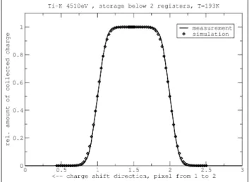
5.1. Comparison with measurements
A comparison of the simulation results with those of measurements delivers the accurancy of the complete simulation process from the electric potential to drift and diffusion of a charge cloud. It will show the error due to the applied simplification to a two dimensional region and the neglection of electrostatic repulsion. Figures 18 and 19 show a good reproduction of the measured results. Apart from the contributions by electrostatic repulsion shown in section 4.2, a two dimensional simulation of the electric potential and the charge drift, diffusion and collection process gives correct results. This is at least true for the middle of a pixel and in charge transfer direction.
6. INTERPRETATION OF RESULTS
The anlysis of the various measurements we made showed which physical parameters have the major influence on the pixel response to the photon interaction position relative to a pixel. On the basis of the results we have now, new measurements can be planned. They can either concentrate on the most relevant physical effects or on an improvement of the measurement precision e.g. means to avoid warping of the mesh due to tensile stress when cooling the mesh together with the pnCCD.
Figure 16.Electric potential in a depth of 70µm along the charge transfer direction. The amplitude of 0.018V is near the thermal voltage of 0.0167V at 193K. In this depth the electric fields begin to split the charge cloud at the border of a pixel.
Figure 17. Electric potential in a depth of 7µm along the charge transfer direction. This depth corresponds to the depth where charge is stored, the dips in the storage minima are caused by the much more positive potential of MOS-gates which insulate the p+ doped register contacts.
Figure 18.Projection of simulated and measured charge collection functions of a 75x75µm2 pixel pnCCD along the transfer direction at 1774eV (W-M) for 193K.
Figure 19.Projection of simulated and measured charge collection functions of a 75x75µm2pixel pnCCD along the transfer direction at 4510eV (Ti-Kα) for 193K.
6.1. Back side illumination
With a a fit of an error function to the measured charge collection function, the effective charge cloud size for both charge transfer and row direction could be determined. Thus, it was possible to determine which physical parameters have the biggest influence on the charge collection process. It is mainly the pixel size but also the drift time of a radiation generated charge cloud as indicated by the larger charge cloud size measured in the 51µm pixel device with larger thickness of the fully depleted substrate. Another effect is the slightly larger measured charge cloud size for the row direction compared to the transfer direction in all used devices. This effect must result from the longer drift time in the channel stop region and will be studied together with simulations of a 2 dimensional cut along the row direction. Measurements with varying back contact voltages and a different charge storage mode are still to be analyzed and compared with device simulations. Electrostatic repulsion at energies below 4510eV and device temperature in the range 153K to 193K both have a much smaller effect on the measured charge cloud size. A change of the charge cloud σin a range of 0.12µm (temperatures 153K and 193K) and 0.4µm (1774eV/486e− and 4510eV/1236e−) was measured. The qualitative expectations of a smaller
charge cloud for lower temperatures and/or photon energies are confirmed but these values are at the limit of our measurement accuracy. Device simulations of the electric potential in a pixel including drift, expansion and collection of a radiation generated charge cloud were used to generate a theoretical charge collection function.
They nearly perfectly reproduce the results of measurements with two different energies and further support the conclusion that the influence of electrostatic repulsion on charge cloud expansion is small for the used energies.
6.2. Front side illumination
Absorption of photons in the front side structure has a clear and expected effect, this operation of the device was for analysis only. Normally, pnCCDs are designed for illumination through the thin entrance window on the back side to obtain optimal low X-ray energy response down to 200eV. We are just at the beginning of analysis of these data. The very good confirmation of the simple absorption model for low energies is in contrast to the rather large error for the W-M 1774eV line which would indicate a 20% lower aluminum thickness. In the first analysis, we used profile cuts of the count maps along the charge transfer direction. Only two hole positions are considered in the simple model in contrast to the many different occuring hole positions in the experiment. To avoid errors of the simple analysis, we need a Monte Carlo simulation considering the measured hole positions and as much known details of the register structure layers as possible. A better analysis can then give reliable information on the depth of the seen insensitive region below the MOS-gates. We will use the obtained result for this depth to improve our device simulations and physical model of the device.
7. SUMMARY AND OUTLOOK
We have successfully made mesh measurements with three different types of pnCCDs and backside illumination.
Our front side illumination measurements with a 75µm pixel pnCCD were also successful. We have developed our own method for a complete analysis of the mesh data. Its reconstruction precision was tested and satisfies our demands on position resolution. With back side illumination, the main parameters that influence charge collection in a pixel are the pixel size and the charge cloud size before eventual separation into neighboring pixels.
The charge cloud size itself mainly depends on the device thickness which together with the back contact voltage determines the drift time before collection in the pixel structure. With nearly the same charge cloud size, the form of the charge collection function mainly depends on the ratioσcharge cloud/pixel size. Device temperature and also the number of signal electrons cause changes of the measured charge cloud size as qualitatively expected but at the limit of measurement accuracy. Numerical device simulations correctly reproduce the measured charge collection function in transfer direction. We will do simulations for the row direction of a pixel to further validate the correctness of our approach. Finally the simulations can be used to have a detailed time resolved look at the charge collection process which is impossible with a measurement. A simple model for photon absorption in the front side structure gives good results for X-rays of 705eV (Fe-L) and 930eV (Cu-L) but a larger than expected error for 1774eV (W-M). At higher energies, the method looses precision due to lower contrast of the count rates as expected. A more sophisticated model including a Monte Carlo simulation of the illumination through mesh holes will be used to obtain more precise results. With a better model of the absorption profile and confirmed layer thicknesses, we can estimate the depth of the insensitive region below the MOS-gates and use the result as an input for device simulations.
ACKNOWLEDGMENTS
The authors wish to thank all people contributing to this paper, especially the technology staff and the electronics group of the semiconductor laboratory of the Max-Planck-Institute.
REFERENCES
1. H. Tsunemi, K. Yoshita, and S. Kitamoto, “New technique of the X-ray efficiency measurement of a Charge- Coupled Device with a subpixel resolution,”Jpn. J. Appl. Phys. 36, p. 2906, 1997.
2. J. Hiraga, H. Tsunemi, K. Yoshita, E. Miyata, and M. Ohtani, “How big are charge clouds inside the Charge- Coupled Device Produced by X-ray photons?,” Jpn. J. Appl. Phys.37, p. 4627, 1998.
3. H. Tsunemi, J. Hiraga, K. Yoshita, E. Miyata, and M. Ohtani, “Comparison of methods of measuring the primary charge-cloud shape produced by an X-ray photon inside the CCD,” Nucl. Instr. and Meth. A439, p. 592, 2000.
4. K. Yoshita, H. Tsunemi, K. C. Gendreau, G. Pennington, and M. W. Bautz, “Direct measurements at the sub-pixel level of the X-ray detection efficiency of the CCD on board the ASCA satellite,”IEEE Trans. Nucl.
Sci. 45, p. 915, 1998.
5. P. Rehak, E. Gatti et al., “Semiconductor drift chambers for position and energy measurements,”Nucl. Instr.
and Meth. A235, p. 224, 1985.
6. L. Str¨uder, H. Br¨auniger et al., “A 36 cm2large monolithic pn-charge-coupled device x-ray detector for the European XMM satellite mission,”Rev. Sci. Instrum. 68, p. 4271, 1997.
7. N. Meidinger et al., “First measurements with a framestore PN-CCD X-ray detector,”Nucl. Instr. and Meth.
A512, p. 341, 2003.
8. R. Hartmann, H. Gorke, N. Meidinger, H. Soltau, and L. Str¨uder, “Results of a fast pnCCD detector system,”
Proc. SPIE 5903 Astronomical Adaptive Optics Systems and Applications II, pp. 59030N–1 – N–9, 2005.
9. N. Meidinger et al., “Systematic testing and results of X-ray CCDs developed for eRosita and other applica- tions,” Proc. SPIE 6276this volume, 2006.