Environmental Control of Charge Density Wave Order in Monolayer 2H-TaS 2
Joshua Hall,
∗,†Niels Ehlen,
†Jan Berges,
‡Erik van Loon,
‡Camiel van Efferen,
†Clifford Murray,
†Malte R¨ osner,
¶Jun Li,
†Boris V. Senkovskiy,
†Martin Hell,
†Matthias Rolf,
†Tristan Heider,
§Mar´ıa C. Asensio,
kJos´ e Avila,
kLukasz Plucinski,
§Tim Wehling,
‡Alexander Gr¨ uneis,
†and Thomas Michely
††II. Physikalisches Institut, Universit¨ at zu K¨ oln, Z¨ ulpicher Straße 77, 50937 K¨ oln, Germany
‡Institut f¨ ur Theoretische Physik, Bremen Center for Computational Materials Science, Universit¨ at Bremen, Otto-Hahn-Allee 1, 28359 Bremen, Germany
¶Institute for Molecules and Materials, Radboud University, 6525 AJ Nijmegen, The
Netherlands
§Peter Gr¨ unberg Institut (PGI-6), Forschungszentrum J¨ ulich GmbH, 52425 J¨ ulich, Germany
kANTARES Beamline, Synchrotron SOLEIL and Universite Paris-Saclay, L’ Orme des Merisiers, Saint Aubin-BP 48, 91192 Gif sur Yvette Cedex, France
E-mail: hall@ph2.uni-koeln.de
Abstract
For quasi-freestanding 2H-TaS
2in monolayer thickness grown by
in situmolecu-
lar beam epitaxy on graphene on Ir(111), we find unambiguous evidence for a charge
density wave close to a 3
×3 periodicity. Using scanning tunneling spectroscopy, we
determine the magnitude of the partial charge density wave gap. Angle-resolved pho- toemission spectroscopy, complemented by scanning tunneling spectroscopy for the unoccupied states, makes a tight-binding fit for the band structure of the TaS
2mono- layer possible. As hybridization with substrate bands is absent, the fit yields a precise value for the doping of the TaS
2layer. Additional Li doping shifts the charge den- sity wave to a 2
×2 periodicity. Unexpectedly, the bilayer of TaS
2also displays a disordered 2
×2 charge density wave. Calculations of the phonon dispersions based on a combination of density-functional theory, density-functional perturbation theory, and many-body perturbation theory enable us to provide phase diagrams for the TaS
2charge density wave as functions of doping, hybridization and interlayer potentials, and offer insight into how they affect lattice dynamics and stability. Our theoretical considerations are consistent with the experimental work presented and shed light on previous experimental and theoretical investigations of related systems.
Keywords
transition metal dichalcogenides, TaS
2, monolayer, charge density wave, layer dependence, doping, hybridization
Condensed matter quantum many-body states are often highly sensitive to stimuli such
as pressure, temperature, or changes in chemical composition. Therefore, the concurrence
of pronounced many-body phenomena in (quasi-) two-dimensional (2d) materials
1–4with
advances in synthesis and vertical heterostructuring
5,6has fueled hopes for controlling elec-
tronic quantum phases on demand.
7These hopes are supported by experiments revealing
electronic phase diagrams of several 2d systems – including Fe-based superconductors
8and
transition metal dichalcogenides (TMDCs)
9–15– to be strongly dependent on dimensionality,
thickness, and substrate. However, the microscopic mechanisms behind these dependencies
often remain elusive and a thorough understanding of how to tune electronic quantum phases
by atomic scale manipulations is largely lacking to date – although being an inevitable re-
quirement for implementation of quantum materials into device applications.
Using the example of the prototypical charge density wave (CDW) material TaS
2, we ex- perimentally and theoretically explore how CDW order is influenced by the control parame- ters doping and hybridization with the substrate. Regarding the latter, this is investigated in monolayer (ML) TaS
2as well as the case of interlayer interaction in bilayer (BL) TaS
2. These parameters add additional dimensions to the phase diagram of TaS
2and allow for quantum phase transitions between different kinds of CDW ordered and distorted states. Based on theoretical modeling, we identify doping and hybridization driven phonon self-energy effects as the microscopic origins of the CDW transitions in the ML.
The material under consideration in the present study is the 2H polytype of TaS
2, where the metal atom coordination is trigonal prismatic. As bulk material, it displays a slightly discommensurate 3 × 3 CDW
16phase with a partial gap,
17–20a CDW transition temperature of 75 K,
21and a transition to a superconducting phase at around 1 K.
22In line with related materials,
9,11,12,23the electronic phase diagram of 2H-TaS
2appears highly layer dependent: when approaching monolayer thickness, the superconducting transi- tion temperature of TaS
2becomes enhanced as compared to the bulk.
13–15,24,25CDW order turns out to depend on the number of layers too, but the monolayer limit remains unclear and controversial until now.
Few experimental works addressed charge order in ML 2H-TaS
2recently. Sanders et al.
26found no CDW when a ML was grown on Au(111) by molecular beam epitaxy (MBE). Also, Yang et al.
14conclude the CDW for ML 2H-TaS
2encapsulated in hexagonal boron nitride to be absent, based on transport measurements. In contrast, Lin et al.
27observed a 3 × 3 superstructure indicative of a CDW for the MBE grown ML on graphene (Gr) grown on 6H-SiC(0001). The situation is puzzling and stimulated several theoretical contributions.
Freestanding undoped ML 2H-TaS
2turns out to be dynamically unstable
27,28and favors
CDW order. Further density functional theory studies show that interaction with substrates
affects the tendency of ML 2H-TaS
2towards CDW formation.
28,29For a doping level consistent with that derived from angle-resolved photoemission of ML 2H-TaS
2on Au(111),
26Albertini et al.
28find the CDW to be suppressed. Shao et al.
30point out that an estimate of the doping level in the ML 2H-TaS
2on Au(111) based on changes in the Fermi surface (FS) may severely overestimate the actual charge transfer through non-linear band distortions as a consequence of hybridization. Correspondingly, Lefcochilos- Fogelquist et al.
29argue that the suppression of the CDW in ML 2H-TaS
2on Au(111) is primarily a consequence of hybridization in consequence of strong S-Au interactions, rather than usual charge doping. However, a clear disentanglement of hybridization and doping effects on CDW order is currently lacking.
Here, we take a close look at this issue and analyze experimentally the absence/presence of CDWs in quasi-freestanding ML 2H-TaS
2at different doping levels, as well as the situation in the BL of 2H-TaS
2. Our theoretical analysis is not only fully consistent with the results of our experiments but also resolves apparent discrepancies in the experimental and theoretical works by clarifying the roles of hybridization, doping and interlayer interaction for lattice (de-)stabilization and the formation of CDW states.
Results/Discussion
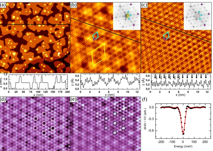
Pristine Monolayer TaS
2Fig. 1 (a) displays a large scale STM topograph of MBE grown TaS
2on Gr/Ir(111) taken at
5 K. The geometrical coverage of 0.7 layers of TaS
2arranges in a network which covers about
65% of the Gr/Ir(111) substrate and readily overgrows a step edge visible in the bottom part
of the image. This network is decorated with about 5% coverage of small triangular islands
in the second layer. As visible in the line profile along the black line in the topograph, the
apparent STM height of ML TaS
2is 6.5 ˚ A. This compares well to both the interlayer distance
measured in bulk 2H-TaS
2of 6.26 ˚ A,
31,32and to our density functional theory calculations
(see Methods).
-200 -100 0 100 200 -0.6
-0.3 0.0
dI/dV / I/V (arb.)
Energy (meV)
(a) (b) (c)
(d) (e) (f)
Figure 1: STM overview of the TaS
2/Gr/Ir(111) sample: (a) Large scale STM topograph of TaS
2islands on Gr/Ir(111). Sample largely covered with ML TaS
2, on which mostly tri- angular second layer islands sit. On the right, a Gr wrinkle is visible, at the bottom right a step edge. The black line shows the position of the line profile at the bottom. (b) Con- stant current STM atomic resolution topograph of ML TaS
2. Three periodic structures are indicated, each with its respective unit cell (Gr/Ir(111) moir´ e yellow, 3 × 3 CDW turquoise, atomic TaS
2lattice violet). Inset: Fourier transform of the STM image with peaks related to the periodicities circled in same the color as unit cell rhomboids. (c) Same image as (b), but with the moir´ e filtered out in Fourier space to enhance the visibility of the CDW. Inset:
Fourier transform of the STM image. The black line shows the position of the line profile at the bottom, where arrows denote the position of the local charge density maximum (see text). (d) Constant height STM topograph of ML TaS
2/Gr/Ir(111) of occupied states. (e) Corresponding constant height STM topograph of unoccupied states. The circles mark the same positions but either show local maxima or minima of the CDW. (f) Constant height tunneling spectrum on ML TaS
2, treated as in Ref. 33. The scale is adjusted to be compa- rable to Fig. 3 (f) and Fig. 4 (b).
Image information [image size, (stabilization) sample bias, (stabilization) tunneling current]:
(a) 200 × 200 nm
2, −1 V, 0.1 nA, (b), (c) 12 × 12 nm
2, −0.15 V, 0.2 nA, (d) 7 × 5 nm
2,
−0.02 V, I
stab= 0.1 nA, (e) 7 × 5 nm
2, 0.02 V, I
stab= 0.1 nA, (f) U
stab= −0.3 V,
I
stab= 0.5 nA.
In Fig. 1 (b), a close-up of the ML TaS
2surface is shown, along with its Fourier transform in the inset. The surface displays three different periodic structures, each being indicated with its respective unit cell in the STM and its corresponding Fourier peak in the inset, respectively.
The largest structure (yellow rhomboid) in the topograph is the moir´ e formed by Gr/Ir(111) which is also visible in the TaS
2layer. Motivated by previous studies on similar TMDC/Gr/Ir(111) systems
34,35we interpret the lack of an additional moir´ e between TaS
2and Gr as a sign for the weak van der Waals (vdW) interaction of the TMDC with its substrate Gr/Ir(111).
Due to the low interaction with the substrate, the TaS
2islands are not strictly epitaxial.
Despite a preferential alignment of the dense-packed TaS
2and Gr rows, orientation scatter is present. For example, in the STM topograph shown in Fig. 1 (b) the orientation mismatch amounts to 4
◦.
The smallest structure (violet rhomboid) is the atomic lattice of TaS
2, which through comparison with the moir´ e can be determined to be (3.37 ± 0.02) ˚ A. It matches well with the bulk in-plane lattice constant found in the literature.
31,32This agreement is consistent with Raman experiments on very similar TMDC/Gr/Ir(111) systems. The investigations have shown that the TMDC layer follows its pristine thermal expansion without indication of strain even after high temperature annealing.
36Therefore, strain is not considered in the following.
The remaining middle-sized periodic structure can be identified as a 3 × 3 superstructure with respect to the atomic TaS
2lattice by filtering out the moir´ e, which is illustrated in Fig. 1 (c). The respective unit cells of the atomic lattice and the 3 × 3 superstructure are indicated in violet and turquoise respectively. In analogy to the bulk counterpart, we associate this 3 × 3 superstructure with a CDW phase of ML TaS
2found at sufficiently low temperatures, and will characterize some of its fingerprints in the following.
It is hard to see the details of the 3 × 3 CDW from the line profile in Fig. 1 (b), as
the profile is dominated by the moir´ e corrugation of about 0.5 ˚ A. Removing the moir´ e in
Fig. 1 (c), allows examination of spatial details of the CDW. Following the black arrows (marking the position of the highest atom in the line profile) from right to left reveals the 3a periodicity, where a is the lattice constant of TaS
2. However, on the left-hand side of the line profile, the 3a periodicity of the highest atoms is drawn by the position of the grey arrows, which are shifted relative to the black arrows. This indicates a phase shift in the CDW consistent with the absence of strict commensurability.
16More details on the interaction of the CDW with island terminations and defects are found in the Supporting Information.
In order to demonstrate the CDW origin of the superstructure, we probe states above and below the Fermi energy by constant height STM and show results in Fig. 1 (d) and (e). A contrast inversion takes place upon change of polarity, as highlighted by the black circles in (d) enclosing brightness maxima and the white circles in (e) enclosing brightness minima. Both sets of circles are located around the same atoms. In a CDW, the occupied and unoccupied states above and below the Fermi energy have the same wave vector k
Fbut different energies, resulting in antiphase behavior in real space. This behavior is clearly reproduced in the respective figures.
Performing scanning tunneling spectroscopy (STS) at 5 K reveals a reduction of the local density of states (LDOS) at the Fermi energy [cf. Fig. 1 (f)], which (to our best knowledge) has not been reported before for ML TaS
2. We associate this feature with partial gapping of the FS similar to the bulk case. Following the methodology of Ref. 33, we divide the dI/dV signal by I/V whereby the features in the LDOS become more pronounced (see Supporting Information). After background subtraction, we find a width of 2∆ = (32 ± 9) meV, where the scatter reflects the variation of the measured CDW gap due to variations of the tip state.
Compared to the data of bulk 2H-TaS
2in which 2∆ = 100 meV,
18,19our gap is signifi-
cantly smaller. To elaborate on this, we note that in previous work the gap size was merely
estimated, while we use a reproducible method described in Ref. 33, which may contribute
substantially to the difference. Ref. 33 points out that in STS on TMDCs the partial CDW
gap may be located very near to features related to the flat d band of the transition metal.
These may be assigned falsely to the CDW gap edge and artificially increase the gap size.
The normalization by I/V helps to disentangle these effects and puts the gap determination on reproducible grounds.
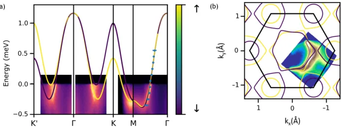
In Fig. 2 (a), angle-resolved photoemission spectroscopy (ARPES) scans in high symme- try directions are shown. The ARPES data indicate a spin-orbit split band in the energy range close to the Fermi level. It is attributed to the Ta d-states, based on literature data for the 2H polytype.
20,37,38The band is composed of a nearly degenerate hole-like pocket around Γ and of spin-split hole-like pockets at the inequivalent K points. Discrete values for the dispersion obtained by standing wave pattern analysis of STS data around Γ are shown as blue dots (see also Supporting Information).
Fig. 2 (b) displays the FS of TaS
2/Gr/Ir(111) measured by ARPES. The hexagonal hole pocket around the center of the Brillouin zone and the spin-split hole pockets around the K-points compare qualitatively well with bulk ARPES results.
37,38We performed a tight-binding (TB) fit of the experimental band structure taking into ac- count all measured experimental ARPES and STS data and treating all TB parameters as mere fit parameters. The fit is represented in Figs. 2 (a) and (b) as lines ranging from yellow to blue in dependence of their spin character. By comparison to the TB fit, the spin-orbit split nature of the band in the ΓK-direction and of the hole-like pockets at the inequivalent K-points become obvious. Overall, the TB fit perfectly reproduces the observed spectra, and the ARPES data display no hybridization between the TaS
2adlayer and its substrate.
From the relative area of the occupied states enclosed by the tight-binding fitted FS,
we calculate the free charge carrier concentration and find 1.10 ± 0.02 electrons per unit
cell, that is an excess or doping of 0.1 electrons per unit cell (in the following denoted as
x = − 0.10) in comparison to half-filling of the band (for details see Methods). As the TB
band structure is a fit to the experimental band structure, the estimate of the doping level
based on it is much more precise than an estimate based on ab initio calculations.
(a) (b)
Energy (meV)
Figure 2: Band structure of ML TaS
2: (a) Tight-binding fit of the band structure based on experimental ARPES and STM (blue dots) data. The color of the calculated bands indicates the spin contribution; yellow: spin up, magenta: spin down. The color scale of the ARPES spectra in the background indicates photoemission intensity from orange (high intensity) to violet (low intensity). (b) Fermi surface as measured with ARPES and tight-binding fit of FS. Color scale of the calculated bands as in (a), color scale of the FS ARPES data in the background indicates photoemission intensity from white (high intensity) to blue (low intensity). ARPES data was taken at about 40 K using 21 eV photon energy, with the exception of the KM direction which was taken at about 100 K and 50 eV photon energy.
In summary, we find slightly doped ML TaS
2to show a CDW state, with a periodicity close to 3 ×3. Both the CDW periodicity and the TB band structure we obtain from ARPES and STS are similar to the bulk counterpart.
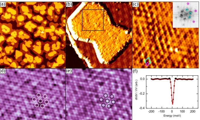
Bilayer TaS
2In Fig. 3 (a), a large scale STM overview of a sample with substantial BL coverage is shown.
The top layer islands grow perfectly aligned to the respective ML TaS
2bottom layer on Gr/Ir(111). We never find the second layer of TaS
2with a rotational misalignment relative to the bottom layer. The strict epitaxial relation of the two TaS
2layers is interpreted as a consequence of a strong interaction between the two layers in the BL case; the absence of the Gr/Ir(111) moir´ e in BL islands is consistent with a stronger interaction of the two TaS
2layers as compared to the Gr-TaS
2interaction.
Fig. 3 (b) shows one of the BL islands in higher resolution which exhibits internal struc-
-200 -100 0 100 200 -0.4
-0.2 0.0
dI/dV / I/V (arb.)
Energy (meV)
(a) (b) (c)
(d) (e) (f)
Figure 3: STM overview of BL TaS
2/Gr/Ir(111). (a) STM overview topograph. (b) Close up of BL TaS
2showing a disturbed 2 × 2 superstructure. The black square indicates the location of panel (c). (c) Constant current STM showing the 2 × 2 superstructure with atomic resolution on BL TaS
2. The respective unit cells (2 × 2 CDW turquoise, atomic TaS
2lattice violet) are shown. Inset: Fourier transform of the STM image with peaks related to the periodicity represented by unit cells circled in same color as unit cell rhomboids. (d) Constant height STM topograph of the occupied states. (e) Corresponding constant height STM topograph of unoccupied states. The circles mark the same positions but indicate either local maxima or minima of the CDW. (f) normalized constant height STS spectrum on BL TaS
2.
33The scale is adjusted to be comparable to Fig. 1 (f) and Fig. 4 (b).
Image information [image size, (stabilization) sample bias, (stabilization) tunneling cur- rent]: (a) 200 × 200 nm
2, 1.5 V, 0.1 nA, (b) 25 × 25 nm
2, −1 V, 1 nA, (c) 8 × 8 nm
2,
−1 V, 4 nA (d) 7 × 5 nm
2, −0.05 V, I
stab= 0.1 nA, (e) 7 × 5 nm
2, 0.05 V, I
stab= 0.1 nA,
(f) U
stab= −0.2 V, I
stab= 10 pA.
ture. This is found to be a 2 × 2 superstructure with respect to the atomic lattice of TaS
2, and is of poor order compared to the 3 × 3 case in the monolayer. Though the atomic lattice does not show an increased defect density, the 2 × 2 periodicity is often only preserved over a few periods and may even be absent in small patches, compare Fig. 3 (c). In (c) the 2 × 2 unit cell and the TaS
2unit cell are indicated. The 2 × 2 superstructure is also visible in the Fourier transform of Fig. 3 (c) shown as an inset.
In analogy to the ML, we investigate the BL superstructure with constant height STM on opposing sides of the Fermi level. A comparison of Fig. 3 (d) and (e) illustrates the out- of-phase behavior of the CDW contrast (the black and white circles again mark the same positions, but are either local CDW maxima or minima). The poorly ordered 2 × 2 thus represents a CDW.
Similar to the ML 3 × 3 CDW, a measurement of the differential conductance shows a reduced LDOS at the Fermi level [cf. Fig. 3 (f)], which is interpreted as a partial CDW gap.
The numerical value of the BL gap width is 2∆ = (18 ± 9) meV, when the same analysis as for the ML is used.
When interpreting the CDW phase transition from 3 × 3 to 2 × 2 in going from the ML to the BL, the different environment of the BL compared to the ML has to be taken into account. To specify, the first layer TaS
2growing on Gr/Ir(111) has a different substrate (i.e.
Gr) than the second layer, which grows on TaS
2as a substrate. Considering the system
ML TaS
2/Gr it can be stated that the interaction between the two layers (and therefore the
hybridization) seems negligible, because: (i) In constant current dI/dV maps standing wave
patterns can be observed (cf. Supporting Information); (ii) ARPES data are not indicative
of any band hybridization. In contrast to this, we assume stronger binding (and therefore
stronger hybridization) of the second TaS
2layer to the first one: (I) Standing wave patterns
are hardly visible in the BL and are strongly distorted; (II) The epitaxial relation between
the second layer and the first layer is strict, while the ML TaS
2islands display orientation
scatter with respect to graphene.
Another factor to consider is the possibility of a surplus of Ta atoms being present in the vdW gap between the two TaS
2layers. This phenomenon of self-intercalation has been observed in bulk TaS
2,
39,40and may provide additional charge. As we will show in the following, this change in doping level might give rise to a modified CDW periodicity.
Though it should be mentioned that evidence for a 2 × 2 ordering has been found in isostructural and -electronic pristine 2H-NbSe
2,
41this structure has not yet been observed in TaS
2.
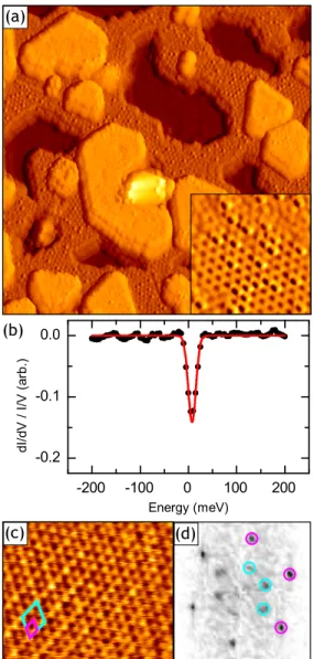
Doped Monolayer TaS
2To investigate the influence of doping on the CDW, TaS
2/Gr/Ir(111) at 500 K is exposed to Li vapor. The STM topograph in Fig. 4 (a) taken after exposure shows distinct features. (A) On the ML TaS
2, a regular superstructure is present, which is enlarged in the inset. Relating this structure to the dense-packed TaS
2directions via the TaS
2lattice allows inference of a ( √
7 × √
7)R19.1
◦superstructure, which we interpret as a result of ordered Li adatom adsorption. (B) The moir´ e of Gr/Ir(111) is no longer visible on the ML TaS
2islands. (C) Li intercalation structures can be observed under Gr. These features lead to the interpretation that Li can be found on TaS
2, under Gr, and presumably also in between Gr and ML TaS
2. The indistinct intercalation distribution impedes a precise Li coverage determination. We estimate 0.2 ML = 2.0 × 10
18atoms m
−1as a lower bound to the total Li coverage. We further performed DFT calculations and estimate an increase of the doping level by 0.25 electrons (x = − 0.25) through Li adsorption with a coverage corresponding roughly to the experimental one, see Supporting Material.
The normalized differential conductance around the Fermi level of the ( √ 7 × √
7)R19.1
◦superstructure of ML TaS
2is shown in Fig. 4 (b). The partial energy gap of size 2∆ = (19 ± 9) meV is strong evidence for a remanent CDW. We note that at the spectroscopy temperature of
5 K the STM tip is not able to remove Li. Only by increasing the temperature to 30 K, the
-200 -100 0 100 200 -0.2
-0.1 0.0
dI/dV / I/V (arb.)
Energy (meV)
(a)
(b)
(c) (d)
Figure 4: Li doped TaS
2: (a) Large scale STM topograph showing the entire sample surface to be covered by Li adatoms. In the inset an ordered ( √
7× √
7)R19.1
◦is visible. (b) Constant height STS spectrum on Li/ML TaS
2/Gr/Ir(111), treated following the methodology of Ref.
33. The scale is adjusted to be comparable to Fig. 1 (f) and Fig. 3 (f). (c) Constant current STM taken at 30 K on ML TaS
2showing atomic TaS
2resolution and 2 × 2 indications, both marked with their respective unit cell. (d) Corresponding Fourier transformation.
Image information [image size, (stabilization) sample bias, (stabilization) tunneling current]:
(a) 60 × 60 nm
2, −0.8 V, 0.1 nA, inset: 10 × 10 nm
2, −0.3 V, 0.1 nA (b) U
stab= −0.15 V,
I
stab= 0.2 nA, (c) 6 × 5 nm
2, 0.01 V, 1 nA.
Li-adlayer could be removed from the ML TaS
2with the STM tip, and the atomic lattice of TaS
2becomes visible. It still exhibits periodic modulations as shown in Fig. 4 (c). Both in the STM topography and in the Fourier transform in Fig. 4 (d) these modulations relate to a poor 2 × 2 superlattice ordering.
We also attempted to remove the adsorbed Li by thermal annealing to 900 K. Unexpect- edly, this did not result in Li desorption, but in a complete change in the morphology of the TaS
2, which is shown in the Supporting Information.
In the literature, bulk TaS
2intercalation compounds show a variety of stable intercalation structures.
42Also, ordered Li intercalation structures were reported
43,44and even preliminary data for 2 × 2 intercalation was mentioned.
43It can therefore not be excluded that the observed 2 × 2 superlattice may relate to intercalant ordering under ML TaS
2. Nevertheless, as no other superstructure is present and a partial gap in the density of states at the Fermi level is found, it is plausible that doping changed the CDW periodicity in the ML from 3 × 3 to 2 × 2.
Theory
In order to understand the microscopic origins of the CDW states observed experimentally, we performed calculations of phonon dispersions based on a combination of density-functional theory, density-functional perturbation theory (DFPT)
45,46and many-body perturbation theory. We calculated the phonon self-energy, Π
~qαβ[see Methods, Eq. (2)], which encodes the renormalization of the phonon dispersion due to interactions of the phonons with the electrons from the TaS
2conduction band. On this basis, we analyze here how the interplay of several external control parameters, i.e. electronic hybridization with substrates, doping, and interlayer potentials, affects lattice dynamics and stability in TaS
2.
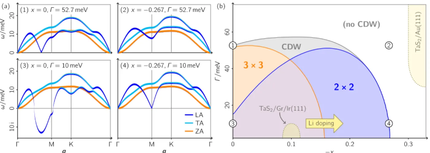
The dependence of the resulting renormalized phonon dispersions in ML-TaS
2on doping and hybridization with a substrate is shown in Fig. 5 (a). In the quasi-freestanding case, i.e.
undoped (x = 0) and weakly hybridized (Γ = 10 meV), the longitudinal-acoustic (LA)
01020
ω/meV
(a) (1)x= 0, Γ= 52.7 meV (2)x=−0.267, Γ= 52.7 meV
Γ M K Γ
10i01020
q
ω/meV
(3)x= 0, Γ= 10 meV
Γ M K Γ
q
(4)x=−0.267, Γ= 10 meV
ZA TA LA
(b)
TaS2/Gr/Ir(111)
TaS2/Au(111)
Li doping
0 0.1 0.2 0.3
204060
−x
Γ/meV
1 2
3 4
(no CDW) CDW
2 × 2 3 × 3
Figure 5: Phonon dispersions and lattice instabilities of ML TaS
2under different electronic conditions at temperature T = 0. (a) Acoustic phonon dispersions for different levels of hybridization with the substrate, Γ (HWHM of the electronic broadening), and charge doping, −x (in units of electrons per Ta atom). x < 0 refers to electron addition. The character of the phonon modes, i.e. longitudinal (LA), transverse (TA), or out-of-plane (ZA), is marked in color. Imaginary phonon mode energies indicate that the lattice is unstable towards corresponding periodic lattice distortions. (b) Phase diagram of lattice instabilities in ML TaS
2. The CDW region is defined by the presence of an imaginary phonon energy at one or more ~ q points. Regions with instabilities at M for the 2 × 2 and at 2/3 ΓM for the 3 × 3 CDW are marked in color. The experimentally realized situations of pristine ML TaS
2/Gr/Ir(111), as well as Li doped as in this work, and ML TaS
2/Au(111) (Ref. 26,30) are located in the phase diagram. Points corresponding to the phonon dispersions shown in (a) are marked with encircled numbers 1–4.
phonon branch exhibits a strong Kohn anomaly. Phonon modes with imaginary energy im-
ply that the lattice is unstable with respect to corresponding periodic distortions and charge
ordering. The density functional theory establishes a local extremum in the Landau energy
functional E(ξ) = E
0+
12ω
~q2ξ
~q2+ . . .. This functional quantifies the energy cost of moving
the atoms out of the DFT equilibrium position by some distortion ξ
~q. The square of the
phonon energy ω
~qis the coefficient of the quadratic contribution to the energy. Therefore,
an imaginary phonon frequency implies an energy gain, which means that the equilibrium
is unstable towards distortions with the corresponding wave vector ~ q. This linear response
theory reveals the existence of instabilities, but it does not predict the distorted structure
(corresponding to the global minimum of the Landau functional). However, the mode with
the largest imaginary frequency, also called leading instability is a clear indicator of energet-
ically particularly favorable distortions. In the quasi-freestanding case, the instability region extends over large parts of the Brillouin zone including the wave vectors ~ q = 2/3 ΓM and M.
At ~ q = 2/3 ΓM, which is associated with the 3 × 3 CDW in the ML, the lattice instability is particularly strong as indicated by a large imaginary phonon frequency.
The doping and hybridization with a substrate can strongly affect the phonon disper- sions, as Fig. 5 (a) shows. In essence, we find that electron doping moves the wave vector of the leading instability, i.e. largest imaginary frequency, from ~ q ≈ 2/3 ΓM to M such that the CDW shifts in wavelength. At electron doping exceeding about 0.27 electrons per TaS
2unit, the lattice becomes dynamically stable, which is in agreement with previous calculations.
28An increase in hybridization on the other hand leaves the wavelength of the leading CDW instability largely unchanged, but weakens the Kohn anomaly and eventually also stabilizes the lattice. Thus, both doping and hybridization trigger a quantum phase transition from CDW to undistorted states of the lattice but via different critical wave vectors. The overall relation between lattice instabilities, doping and hybridization is summarized in the phase diagram shown in Fig. 5 (b).
Applied to the experiments performed here, we can state the following: In the ML TaS
2/Gr/Ir(111) a doping level of x = −0.10 excess electrons per unit cell is measured in ARPES, while no signs of hybridization are experimentally observed. We therefore locate the ML TaS
2/Gr/Ir(111) in the phase diagram of Fig. 5 (b) in the region around x = − 0.10 and Γ → 0, which is in line with the 3 × 3 CDW observed in STM. Intercalating Li increases the doping and moves the experiment towards the right-hand side of the diagram. This is consistent with the experimental observation of a 2 × 2 CDW in the Li-doped system.
Previous experiments
26on ML TaS
2/Au(111) did not find any charge order down to
4.7 K. A major difference to the experiments reported here, including those with Li interca-
lation, is significant hybridization of the TaS
2with the Au(111) substrate.
30Our calculations
show that hybridization can be very effective at destabilizing charge order. The hybridiza-
tion affects the phonon dispersions through the phonon self-energy Π
~qαβ, Eq. (2), and is much more effective in quenching Π
~qαβthan thermal broadening (see Methods). For ML TaS
2/Au(111), the hybridization is energy-dependent
30and the half-width at half-maximum (HWHM) broadening Γ spans a range between 30 meV and 90 meV. We have based our estimate for the electronic broadening on the results of Ref. 30, which contains DFT results for TaS
2with and without Au(111) substrate. A broadening of 30 meV explains the change in spectral weight at the Van Hove singularity, and a broadening of up to 90 meV is needed to describe the transfer of spectral weight into the gap. Placing ML TaS
2/Au(111) in the phase diagram of Fig. 5 (b) we have to account for both the electron (pseudo-)doping
30in the range between x = − 0.3
26and −0.4
30and the hybridization between Γ = 30 meV and 90 meV. Clearly the interplay of both stabilizes the lattice. Lattice relaxation can further support this stabilization.
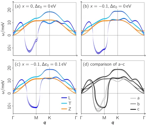
28,29Calculated phonon dispersions of freestanding undoped BL 2H-TaS
2are shown in Fig. 6 (a).
The dispersion and in particular the instability regions in freestanding undoped BL [cf.
Fig. 6 (a)] are indeed very similar to the corresponding ML case [cf. Fig. 5 (a)]. Thus, it is a priori unexpected that BL TaS
2/Gr/Ir(111) features a 2 × 2 CDW in contrast to the 3 × 3 CDW in ML TaS
2/Gr/Ir(111) and also to the 3 × 3 CDW in bulk TaS
2.
What could drive the CDW order in the BL towards 2 × 2? First, as in the ML case,
charge doping could be responsible. Since direct interaction in the bilayer with the substrate
is limited to the bottom layer, stronger average charge doping as in the monolayer due to
interaction with the substrate is unlikely. A possible cause of stronger average charge doping
could be different defect densities in the monolayer and in the bilayer case. Clearly, in the
BL the doping from and hybridization with the substrate are naturally different for the
bottom and top layer. Also, doping due to defects within the layers can be different for each
layer due to inequivalent local growth conditions. Such asymmetries between bottom and
top layer might affect CDW formation. In our model, asymmetries of this kind are most
simply accounted for in terms of an interlayer bias potential ∆
0(energy gain −∆
0/2 or
penalty +∆
0/2 for an electron residing in the bottom or the top layer), the effect of which is illustrated in Fig. 6 (b) and (c). We find that the interlayer bias can flatten the phonon dispersion in the regions of the instability and eventually also shift the ~ q vector of the leading instability from ~ q = 2/3 ΓM towards M. Thus, an effective interlayer bias could also explain the observation of the 2 ×2 CDW in the BL regions. Whether additional doping or interlayer asymmetries are the cause for the switching from 3 × 3 to 2 × 2 CDW in the bilayer case in our experiments remains speculative.
10i01020
ω/meV
(a) x= 0,∆ε0= 0 eV (b)x=−0.1,∆ε0= 0 eV
Γ M K Γ
10i01020
q
ω/meV
(c)x =−0.1,∆ε0= 0.1 eV
Z T L
Γ M K Γ
q (d) comparison of a–c
c b a
Figure 6: (a–c) Dispersions of the acoustic phonon branches of BL 2H-TaS
2at different levels of charge doping x and interlayer bias potential ∆
0for a fixed broadening Γ = 1 meV.
(d) Direct comparison of the dispersions from panels (a–c).
Conclusion
Quasi-freestanding monolayer 1H-TaS
2on Gr/Ir(111) displays a 3 × 3 CDW, while bilayer
2H-TaS
2on the same substrate exhibits a less well ordered 2 × 2 CDW. The CDW gaps
the band structure and the FS were determined with ARPES. No indication of hybridization between Gr and TaS
2is present. Using a TB fit to the ARPES data and the dispersion of states near Γ obtained from standing wave patterns in STS maps, a doping of 1.10 ± 0.02 electrons per unit cell is deduced.
Exposure to Li vapor causes a ( √ 7 × √
7)R19.1
◦adatom superstructure on top of mono- layer 1H-TaS
2, presumably accompanied by intercalation. A 2 × 2 periodicity measured after removal of the adatom phase together with a partial gap of 2∆ = (18 ± 9) meV imply the presence of a 2 × 2 CDW.
Our theoretical analysis reveals the microscopic contributors behind CDW (de-)stabilization and the experimentally observed changes in periodicity. It emphasizes the importance of en- vironmental embedding in the study of 2d materials: the theoretically derived CDW phase diagram of TaS
2as a function of doping and hybridization shows that both can suppress CDW order. The critical wave vectors ~ q
cof the associated quantum phase transition from the CDW to the undistorted lattice depend on the stimulus driving CDW destabilization and are ~ q
c= 2/3 ΓM, and ~ q
c= ΓM in the doping and hybridization driven case, respectively.
In the BL TaS
2case the experimental finding of 2 × 2 charge order is surprising given that the phonon dispersion of freestanding pristine BL TaS
2is very similar to that of the ML. Our analysis shows that an interlayer potential can push the preferential CDW ordering vector towards ΓM, which could explain the observed 2 × 2 order. Additional charge from self-intercalated Ta in the vdW gap could be responsible for this phonon renormalization, but this remains speculative.
Quite generally, our results demonstrate that phase diagrams of van der Waals het-
erostructures are high-dimensional due to the all surface nature of the constituents. Ev-
ery interface, either between van der Waals bound 2d layers or between 2d layers and a
three-dimensional substrate allows additional control parameters to enter the stage – control
parameters that could be made operative in heterostructure based devices.
Methods/Experimental
TaS
2/Gr/Ir(111) samples are grown in situ as described in detail Ref. 34. In short, the Ir(111) crystal is cleaned by grazing incidence 4.5 keV Xe
+ion exposure and flash anneal- ing to 1500 K. Subsequently, a layer of single-crystalline Gr is grown via temperature pro- grammed growth with ethylene.
47The TaS
2growth is performed by Ta evaporation in a sulfur background pressure, followed by annealing to 1000 K, again in a sulfur background pressure. We measure the resulting coverage in ML, where one ML refers to the one-unit-cell S-Ta-S triple layer, which for TaS
2contains 1.02 × 10
19Ta atoms m
−1. Growth conditions are tuned to optimize epitaxy for ARPES or to promote bilayer growth.
The TaS
2layers are checked by low energy electron diffraction and analyzed by STM and ARPES. STM is performed both in a variable temperature (30 K – 700 K) STM apparatus and in a low-temperature system at 5 K. If not otherwise indicated, all STM data are taken at 5 K. The software WSxM
48was used for STM data processing.
For STS we use standard lock-in technique with modulation frequency of 777 Hz and modulation amplitudes V
mod= 4 mV
rms. For point spectra and constant height topographs U
staband I
stabof stabilization are indicated.
ARPES spectra were recorded using photons of hν = 21.11 eV from a standard He discharge lamp with the sample at 40 K, and synchrotron light at the ANTARES end station of the SOLEIL synchrotron using 50 eV photon energy with the sample at 100 K.
The tight-binding fit was conducted using the quasi-Newton L-BFGS algorithm
49to minimize the difference in energy between the ARPES peaks of the d-type TaS
2band and the TB result. The TB model is an adapted version of ML MoS
2models in literature
50as the atomic structure is the same. As a starting point for the fit, MoS
2fit parameters were adopted
50with modified on-site energies to shift the Fermi level inside the d-type band.
To determine the doping level, we started from the TB calculated FS, rather than the
experimentally measured FS. If one would determine the area of the FS simply from the
in the FS can be significant, an accurate fit is difficult if the bands come too close to each other. This reduces the accuracy of the overall area hypothetically determined via this method. The TB model, on the other hand, is a physically reasonable parameter fit that takes into account all ARPES data for the occupied states and the STM data for occupied and unoccupied states. This simplifies the determination of the correct band positions and increases the accuracy of the determined FS area.
A spin-orbit split band in a crystal with N unit cells has N k-values, which are uniformly distributed within the first Brillouin zone. Each of the two spin-orbit split subbands has N electron states. In case of the spin-orbit split d-derived band in TaS
2, the area A
FS,h,↑of the hole pockets around the Γ and K points for the spin-up subband compared to the area A
BZof the first Brillouin zone represents thus the degree of band filling of that d-state derived subband, i.e. the number of holes n
h,↑per unit cell in that subband. The number of electrons n
e,↑in that subband and per per unit cell is then simply n
e,↑= 1 − n
h,↑. The same procedure is conducted for the d-derived spin-down subband. The total number of electrons in the spin-orbit split band is thus
n
e= (1 − n
h,↑) + (1 − n
h,↓) = 2 − A
FS,h,↑+ A
FS,h,↓A
BZ(1)
and amounts to n
e= 1.10 ± 0.02.
The goal of our theoretical modeling is to understand the influence of different external
stimuli such as hybridization with substrates or electron doping on the TaS
2phonon disper-
sion and thereby on the lattice instabilities which emerge from the softening of longitudinal-
acoustic phonons due to metallic screening. To this end, we downfold the electronic struc-
ture and lattice dynamics of 2H-TaS
2to a material-realistic low-energy model containing
all phonons and the partially filled electronic conduction band. The phonons entering this
model are bare (or, more precisely, partially screened) in the sense that they have to be renor-
malized due to interactions with electrons from the conduction band.
46The corresponding
bare phonons and the corresponding bare dynamical matrix D are obtained from constrained DFPT,
46where constrained means that screening within the low-energy electronic subspace is excluded in the determination of the phononic properties. The final experimentally ob- servable phonon dispersion results from the renormalized dynamical matrix D e = D + Π, which accounts for mutual coupling of the lattice vibrations and the low-energy electronic degrees of freedom through the phonon “self-energy”:
Π
~qαβ= 2 N
X
~knm
e g
~qα~knmf(
~k+~qm) − f (
~kn)
~k+~qm−
~kng
∗~
qβ~knm