Single NdPc 2 Molecules on Surfaces:
Adsorption, Interaction, and Molecular Magnetism
I n a u g u r a l - D i s s e r t a t i o n zur
Erlangung des Doktorgrades
der Mathematisch-Naturwissenschaftlichen Fakultät der Universität zu Köln
vorgelegt von Sarah Fahrendorf
aus Marl
Berichterstatter: PD Dr. D. E.Bürgler (Gutachter)
Prof. Dr. T.Michely
Tag der mündlichen Prüfung: 24.01.2013
Kurzzusammenfassung
Molekulare Nanomagnete, auch Einzelmolekülmagnete genannt, nehmen eine Schlüssel- rolle in dem aufstrebende Forschungsgebiet der molekularen Spintronik ein. Sie bilden die Grundbausteine für eine Weiterentwicklung spin-elektronischer Elemente der klassi- schen Spintronik zur molekularen Spintronik und könnten in molekularen Spinventilen, molekularen Spintransistoren oder als Quantenbits in Quantencomputern zur Anwendung kommen. Molekulare Nanomagnete sind gekennzeichnet durch hohe Grundzustände der Spinquantenzahl und eine Aufspaltung der Zustände im Nullfeld. Die dadurch entstehenden hohen Relaxationsbarrieren führen zu einer langen Relaxationszeit der Magnetisierung.
Moleküle aus der Klasse der Doppeldecker Phthalocyanine mit einem einzigen Zentrali- on aus der Untergruppe der Lanthanoide (LnPc
2) eingebettet zwischen zwei organische Phthalocyanin (Pc) Liganden sind von hoher Relevanz für das grundlegende Verständnis molekularer Nanomagnete. Der Einfluss von Substraten oder Elektroden auf adsorbierte Moleküle spielt ein zentrale Rolle bei der Entwicklung von Bauteilen für die molekulare Spintronik, da sich die elektronischen und magnetischen Eigenschaften der Moleküle verän- dern können. Ein umfassendes Verständnis des Substrateinflusses ist daher unerlässlich für eine Weiterentwicklung des Forschungsgebietes.
In dieser Doktorarbeit werden aus diesem Grund die elektronischen und magnetischen Eigenschaften des adsorbierten Neodym Doppeldecker Phthalocyanins (NdPc
2) mittels Tieftemperatur-Rastertunnelmikroskopie und -spektroskopie (RTM und RTS) untersucht.
Hierfür werden zunächst die NdPc
2Moleküle unter Ultrahochvakuum-Bedingungen auf verschiedene Oberflächen aufgedampft. Es ergibt sich, dass sich ein hoher Anteil an Doppeldecker Molekülen bei der Deposition in einzelne Phthalocyanine zerlegt. Die Rate der zerstörten Doppeldecker ist dabei stark von der Art des Substrats abhängig. Aus diesem Grund wird die Schlussfolgerung gezogen, dass die elektronische Beschaffenheit der Oberfläche einen stabilisierenden oder destabilisierenden Einfluss auf die intra-molekularen Bindungen hat. Es stellt sich heraus, dass Ladungstransfer von der Oberfläche in die Orbitale des Moleküls ein möglicher stabilisierender Effekt sein könnte.
Eine detaillierte Studie der elektronischen und magnetischen Eigenschaften des adsor-
bierten NdPc
2Moleküls wird auf dem Substrat Cu(100) vorgenommen. Im Rahmen der
Interpretation werden die Ergebnisse der experimentellen RTM- und RTS-Untersuchungen
mit Dichtefunktionaltheorie (DFT) Rechnungen verglichen. Diese DFT-Rechnungen wur-
den von Mitarbeitern des Peter Grünberg Instituts (PGI-1) am Forschungszentrum Jülich
ausgeführt. Es zeigt sich, dass der untere Pc-Ligand des NdPc
2Moleküls robuste chemische
Bindung mit Cu(100) eingeht und seine elektronischen Zustände mit denen der Oberfläche stark hybridisieren. Zugleich ist der Einfluss des Substrats auf die Zustände des oberen Pc-Liganden verschwindend und sie behalten ihren molekülartigen Charakter. Diese mo- lekülartigen elektronischen Zustände können durch ein äußeres elektrisches Feld auf der Energieskala verschoben werden. Das zentrale Ergebnis dieser Studie ist jedoch der direkte Zugriff auf die spin-polarisierten 4f-Zustände des zentralen Nd Ions mithilfe der Rastertun- nelmikroskopie. Der direkte Zugang zu diesen Zuständen ist eine besondere Eigenschaft des NdPc
2Moleküls im Vergleich zu analogen Spezies mit Lanthanoiden höherer Ordnungszahl als Zentralion und erlaubt rein elektrische Schreib- und Lesevorgänge des Spinzustands des Moleküls.
In Hinblick auf Untersuchungen der magnetischen Eigenschaften des NdPc
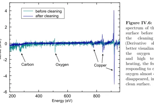
2Moleküls werden spin-polarisierte RTM-Messungen an der zweiten Atomlage von Fe auf W(110) durchgeführt. Die eingesetzten Cr Spitzen werden ex-situ, anhand eines elektrochemischen Verfahrens von Cr Stäben heruntergeätzt. Weitere in-situ Präparationsschritte zeigen zudem keinen grundlegenden Einfluss auf die magnetischen Eigenschaften der Spitze.
Die Etablierung der reproduzierbaren Präparation der ferromagnetischen Fe Oberfläche und der RTM-Spitzen bildet die Voraussetzung für die weiteren Messungen an adsorbier- ten NdPc
2Molekülen mittels spin-polarisierter RTM. Vorläufigen Ergebnisse von RTM- Untersuchungen geben Hinweise darauf, dass ein direkter Zugang zu den spin-polarisierten 4f -Zuständen auch nach Adsorption des Doppeldecker Moleküls auf der zweiten Atomlage von Fe auf W(110) möglich ist.
iv
Abstract
Single molecule magnets (SMMs) play an important role in the field of molecular spintronics.
They have huge potential for application in molecular-spin-transistors, molecular-spin- valves, and molecular quantum computing. SMMs are characterized by high spin ground states with zero-field splitting leading to high relaxation barriers and long relaxation times.
A relevant class of molecules are the lanthanide double-decker phthalocyanines (LaPc
2) with only one metal atom sandwiched between two organic phthalocyanine (Pc) ligands.
For envisaged spintronic applications it is important to understand the interaction between the molecules and the substrate and its influence on the electronic and magnetic properties.
The subject of this thesis is the investigation of the adsorbed neodymium double-decker phthalocyanine (NdPc
2) by means of low temperature scanning tunneling microscopy and spectroscopy (STM and STS).
The molecules are deposited by sublimation onto different substrates. It is observed that a large fraction of the double-decker molecules decomposes during deposition. The decomposition probability strongly depends on the chosen substrate. Therefore it is concluded that the substrate modifies the electronic structure of the molecule leading to a stabilization or destabilization of the molecular entity. Charge transfer from the surface to the molecule is identified as a potential stabilizing mechanism.
The electronic and magnetic properties are investigated in detail for adsorbed NdPc
2molecules on Cu(100). The results of the experimental study are compared to state-of- the-art density functional theory calculations performed by our colleagues from the Peter Grünberg Institute (PGI-1) at the Forschungszentrum Jülich. Interestingly, the lower Pc ring of the molecule hybridizes intensely with the substrate leading to strong chemisorption of the molecule, while the upper Pc ring keeps its molecular type electronic states, which can be energetically shifted by an external electric field. Importantly, it is possible to get direct access to the spin-polarized 4f -states of the central Nd ion by means of STM and STS. This important and unique characteristic absent for late lanthanide double-decker phthalocyanine molecules opens the door for direct reading and writing of the molecular spin-state by purely electrical means.
In view of the intended investigations of the magnetic properties of the NdPc
2molecule
coupled to ferromagnetic surfaces, spin-polarized STM investigations of the second atomic
layer of Fe on W(110) are performed. Here, bulk Cr-tips are used, which were ex-situ
electrochemically etched from a Cr rod. Further in-situ treatment is shown to have
no essential influence on the magnetic properties of the tips. The reproducible and
reliable preparation of the ferromagnetic substrate and the Cr-tips is the basis for further investigations of the NdPc
2molecule adsorbed on the second atomic layer of Fe on W(110).
Preliminary STM and STS results give strong evidence, that the direct access to the spin-polarized 4f -states is also feasible after adsorption of the double-decker molecule on a ferromagnetic substrate.
vi
Contents
I Introduction 1
II Molecules in Spintronics 5
II.1 Molecules with Magnetic Properties . . . . 5
II.1.1 Single Molecule Magnets . . . . 6
II.2 Adsorption on Surfaces . . . . 7
II.3 Magnetic Molecules on Surfaces . . . . 9
II.4 NdPc
2Double-Decker Molecule . . . . 9
III Scanning Tunneling Microscopy 13 III.1 The One Dimensional Tunneling Effect . . . . 14
III.2 Interpreting STM Images . . . . 16
III.3 Probing the Local Density of States . . . . 18
III.4 Spin-Polarized Tunneling Experiments . . . . 20
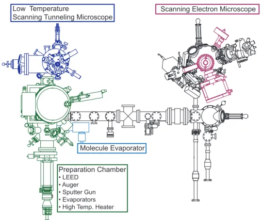
IV Experimental Methods 25 IV.1 Vacuum System . . . . 25
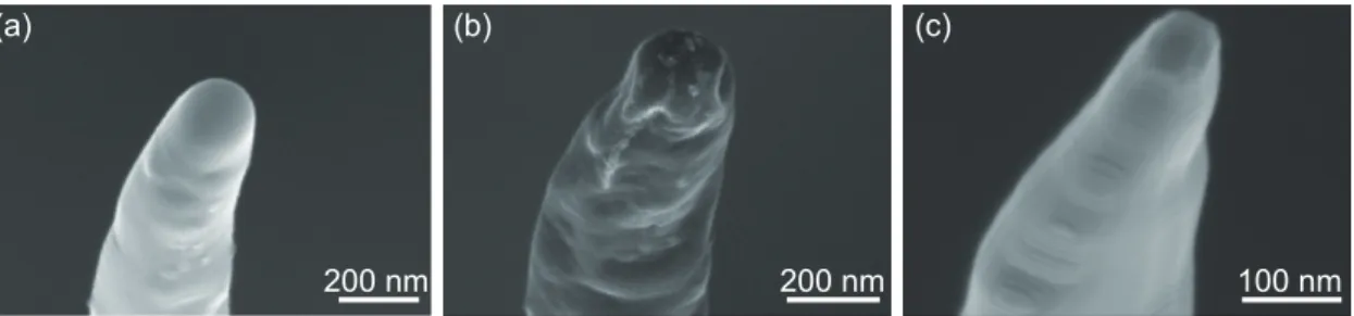
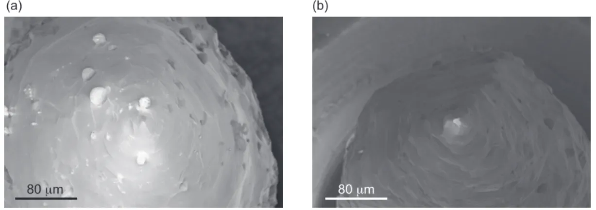
IV.2 Tip Preparation . . . . 27
IV.2.1 Tungsten Tips . . . . 27
IV.2.2 Chromium Tips . . . . 28
IV.3 Sample Preparation . . . . 33
IV.3.1 Sputtered Samples . . . . 33
IV.3.2 HOPG . . . . 34
IV.3.3 Iron on Tungsten . . . . 34
IV.4 Molecules . . . . 36
V Adsorption of NdPc
2on Surfaces 39 V.1 Surface-Dependent Adsorption . . . . 40
V.1.1 Cu(100) . . . . 41
V.1.2 Fe on W(110) . . . . 43
V.1.3 Au(111) . . . . 44
V.1.4 Au(100) . . . . 46
V.1.5 HOPG . . . . 47
V.2 Discussion . . . . 47
Contents
VI NdPc
2Spin-Polarized 4f -States Accessed by STM 51
VI.1 Adsorption of NdPc
2on Cu(100) . . . . 51
VI.2 Electronic Structure of the Adsorbed NdPc
2. . . . 55
VI.3 Conclusion and Perspectives . . . . 61
VII Iron on Tungsten 63 VII.1 Previous Results . . . . 64
VII.1.1 Topography . . . . 64
VII.1.2 Electronic and Magnetic Properties . . . . 65
VII.2 SP-STM Investigations on the 2nd Monolayer of Fe on W . . . . 68
VII.2.1 Mapping the Surface . . . . 68
VII.2.2 Out-of-plane Domains . . . . 69
VII.2.3 Domain Wall Investigations . . . . 72
VIII NdPc
2Adsorbed on Fe on W(110) 77 VIII.1 Topographic and Electronic Structure . . . . 78
IX Summary and Outlook 85
Bibliography 89
Acknowledgement 99
Curriculum Vitae 103
viii
CHAPTER I
Introduction
The continuos demand for increasing information processing capacity and data storage density leads to an ongoing miniaturization of electronic devices that will in the near future hit physical limitations at the current technologies. In view of this upcoming challenge new materials for advanced technologies with high densities and low energy consumption have to be developed. One promising pathway is focussing on the ultimate molecular limit by integrating molecules into electronic devices [1]. The conventional top-down fabrication process of electronic devices reaches its limits at a scale of the wavelength of the light used in the photolithography procedure. In contrast to this, molecules consisting of only tens of atoms can be implemented in devices using bottom-up processes, which does not rely on any lithography.
In the research field of molecular electronics [2], transport through molecular orbitals is studied by connecting molecules to nanoelectrodes. In these measurements, quantum effects as for instance the coulomb-blockade can be observed [3]. Molecules offer some general properties that make them well suited for the integration into electronic devices.
The synthesis of organic molecules with sizes down to a few Å in large quantities and with perfect reproducibility is possible at low cost. By means of chemical synthesis certain functionalities such as the coupling to electrodes, the magnetism or the transport properties can be easily tailored [4, 5]. Furthermore, they show the ability of self organization on appropriate substrates which makes the realization of molecule chains or arrays on surfaces feasible [6].
Combining the field of molecular electronics with the field of spintronics by integrating
molecules with magnetic properties into the devices offers the spin of an electron as an
additional degree of freedom [7, 8]. Setting, manipulating, and detecting of spins allows
using the electron spin rather than the electron charge as a state variable for information
processing. Depending on the spin-state of the electron it for instance interacts differently
with magnetic material [9–11]. Entities with stable magnetic moment furthermore maintain
their spin-state between manipulation steps, i.e. they show non-volatility. Spin-states
can be controlled by applying external magnetic fields, spin-polarized currents or even
I Introduction
light [12]. The switching processes in general cost less energy the lower the number of manipulated spins is. In magnetic molecules the number of spins is orders of magnitudes smaller than in lithographically defined nanomagnets.
In the combined research field called molecular spintronics one or more molecules with magnetic properties are integrated into molecular devices with spintronic functionalities such as e.g. molecular spin-valves [7]. A relevant class of molecules for molecular spin- tronics are the single molecule magnets (SMMs). SMMs act like permanent magnets on the molecular level, which means that they show zero field splitting with an anisotropy direction leading to a slow relaxation of the magnetization [13]. This makes them in addition perfectly suited as qubits for quantum computing [14]. They combine some characteristics of ferromagnetic bulk materials with advantages of the molecular scale:
molecules are perfectly monodispers, whereas nanoparticles for instance vary in shape, size, and magnetic anisotropy. Moreover they typically consist of organic ligands surrounding one or more metal centers with unpaired electrons, which make up the total magnetic moment [13]. This means that only a few electron spins have to be manipulated in order to switch the magnetization of the molecule. Low energy consumption for the switching and manipulating processes is therefore expected.
For the implementation of molecules into electronic devices they have to be deposited on substrates and connected to electrodes. Due to the small molecular structure consisting of only a few tens of atoms in total the influence of an extended substrate on the electronic structure of the molecule becomes significant. This might also change the magnetic proper- ties. Therefore a fundamental understanding of the influence of the substrates on adsorbed molecules is crucial for the further development of molecular spintronics. This requires a combination of experimental results with theoretical calculations. However, the comparison of experiment and theory is only possible if the investigated system is well defined. Scanning tunneling microscopy (STM) and spectroscopy (STS) in ultra high vacuum are versatile tools regarding this requirement: isolated molecules adsorbed on atomically clean and well defined crystalline surfaces are investigated with an atomically sharp tip that allows gaining insight into the electronic properties with high spatial resolution.
In this thesis the adsorption characteristics of molecules with magnetic properties deposited on various surfaces are addressed. In particular the mononuclear early lanthanide double- decker phthalocyanine complex NdPc
2is investigated via STM and STS. It is a promising candidate for being an SMM, since some of its late lanthanide analogues like the TbPc
2complex are already known to show SMM properties [4].
The NdPc
2molecules are synthesized by Dr. Claire Besson of the chemistry group of Prof. Dr. Paul Kögerler of the Forschungszentrum Jülich and RWTH Aachen. For a detailed study, the experimental STM and STS results are compared to state-of-the-art density functional theory calculations carried out by Dr. Nicolae Atodiresei and Dr. Vasile Caciuc from the Peter Grünberg Institute of the Forschungszentrum Jülich. The magnetic properties of the adsorbed molecule are addressed by spin-resolved calculations as well as
2
preliminary spin-polarized STM and STS measurements.
In the beginning of this thesis the theoretical background for the STM study of single molecules with magnetic properties is given. Chapter II introduces the concept of molecular magnetism and possible molecule-surface interactions. The explanations concentrate on aspects, which are crucial for the interpretation of the experimental and theoretical results.
Afterwards the theory of STM and STS as well as spin-polarized STM (SP-STM) is presented in Chapter III.
Chapter IV gives experimental details including the vacuum system, sample preparation and STM-tip preparation. The focus in this Chapter lies on the reproducible ex-situ and subsequent in-situ preparation procedure of bulk Cr-tips for SP-STM measurements.
The experimental results are presented in the next four Chapters. As a starting point the substrate dependence of the adsorption of the NdPc
2molecule is discussed for various surfaces in Chapter V. A detailed analysis of the electronic and magnetic structure of the adsorbed NdPc
2molecule is then given for the case of a Cu(100) substrate. The results of this combined experimental and theoretical study are presented in Chapter VI. In view of SP-STM and STS investigations of the adsorbed NdPc
2complex the ferromagnetic surface Fe on W(110) is subject of Chapter VII in order to introduce this surface as a ferromagnetic substrate and to demonstrate our ability to perform spin-polarized STM and STS experiments. The measurements concentrate on the out-of-plane domains and in-plane domain walls of the second atomic layer of Fe on W(110). This surface layer serves as a ferromagnetic substrate for the preliminary SP-STM study of the adsorbed NdPc
2presented in Chapter VIII.
In Chapter IX the experimental and theoretical results are summarized and evaluated.
Finally an outlook on potential subsequent experiments is given.
CHAPTER II
Molecules in Spintronics
Implementing molecules with intrinsic magnetic moment into conventional spintronic devices has attracted a great deal of interest [7]. It has just recently been shown that molecules with magnetic moments, namely TbPc
2, attached to a carbon nanotube can function as a spin-valve device at the molecular level [15]. One of the main topics in investigating single molecules for spintronic applications is the interaction between these molecules and the surroundings for instance the substrate. Adsorption on metallic surfaces has a large influence on the electronic and therefore also the magnetic properties of the adsorbed molecule. In the following Sections the characteristics of molecules with magnetic properties are introduced. In addition an introduction about chemical bonding is given to provide the basis for the interpretation of the results. Furthermore a short overview about possible interactions of magnetic molecules with surfaces is given, and finally in the last Section, the NdPc
2double-decker phthalocyanine molecule investigated in this work is described to provide the information necessary for the analysis of the experimental and calculated data.
II.1. Molecules with Magnetic Properties
It is possible to classify molecules, depending on their response to external magnetic fields.
Diamagnetic molecules will be repelled by external magnetic fields, due to the induced
magnetic moment that causes a magnetic field opposite to the external one. In contrast
to this, paramagnetic molecules will be attracted and their intrinsic magnetic moment
aligns with the direction of the applied external field. In contrast to the diamagnetic
molecule, the paramagnetic molecule comprises orbitals with un-paired spins, causing the
intrinsic magnetic moment. For spintronic application one relevant class of molecules are
the so called single molecule magnets (SMM) functioning as magnets on the molecular
scale [7, 13].
II Molecules in Spintronics
II.1.1. Single Molecule Magnets
SMMs show a combination of characteristics of classical magnets with properties of quantum systems, such as transport through well defined molecular orbitals and quantum tunneling of the magnetization. SMMs are paramagnetic molecules with the addition of a zero field splitting and a slow relaxation of the magnetization. That means that similar to a conventional ferromagnetic material with long range order, they show an anisotropy direction of the magnetic moment and a certain relaxation time. Depending on the temperature and time-scale, on which the molecules are studied, they can be referred to as SMM and superparamagnetic-like molecule. Their magnetic properties can be described by the Hamiltonian
H = DS
z2+ E(S
2x+ S
y2) + gµ
Bµ
0S · H (II.1) with D and E being the anisotropy constants, gµ
Bµ
0S · H describing the Zeeman energy generated by the applied magnetic field H and S
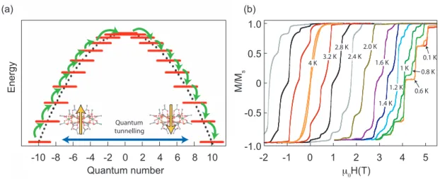
irepresenting the spin components of the system. Figure II.1 (a) illustrates the energy landscape of an SMM. Here the anisotropy constant D is negative and we assume the easy axis to be in z-direction. The potential barrier height is then given by DS
z2and consists of (2S + 1) energy levels indicated in the figure by the red lines. A magnetization reversal occurs for example by thermal excitations over all (2S + 1) energy levels as shown in Fig. II.1 (a) by the green arrows climbing up and down over the potential barrier or via quantum tunneling of the magnetization [13].
The energy levels of the two wells are shifted with respect to each other when an external field is applied. At certain resonance fields where two levels align at the same energy, the electron spin can flip its direction by direct tunneling into energy levels on the other side of the double-well potential as indicated by the blue arrow in Fig. II.1 (a). The quantum tunneling can be directly observed in Fig. II.1 (b), in which hysteresis loops for various temperatures between 4 and 0.1 K are shown. Characteristic steps, indicating a change in the magnetic state of the molecule due to resonant tunneling, are observed at resonant field values. With decreasing temperature the hysteresis loops become broader due to the reduced thermally activated magnetization reversal. For temperatures below 0.6 K the hysteresis loops become temperature independent and do not change their shape and saturation field anymore. Here, the magnetization reversal is by quantum tunneling of the magnetization only.
Chemically, SMMs consist of an inner magnetic center of one or more magnetic atoms and a surrounding organic ligand system. The magnetic atoms can for instance be transition metal atoms like Fe in the {Fe
4} compound [16] and Mn in the {Mn
12} SMM [17] as well as rare earth atoms like Tb in TbPc
2molecules [4]. The organic ligands can be chemically functionalized to alter the coupling of the molecule to the environment and to enhance the magnetic properties, for example to increase the blocking temperature and relaxation times [18]. The coupling to the environment is one of the main challenges in controlling the magnetic properties of adsorbed SMMs. Therefore it is crucial to understand the fundamental properties of adsorbed magnetic molecules. The next two Sections give an
6
II.2 Adsorption on Surfaces
Quantum tunnelling
4 K 3.2 K 2.8 K
2.4 K 2.0 K
1.6 K
1.4 K 1.2 K
1 K 0.1 K 0.8 K 0.6 K
(a) (b)
Energy
Quantum number μ0H(T)
M/Ms
-2 8 4 5
0.5
2
-1 0 1 3
2 -1.0 0 -4 -6 -8
-10 -2
1.0
0
4
-0.5
10 6
Figure II.1.:(a) Schematic representation of the potential barrier separating the two spin ground states of an SMM. Magnetization reversal can occur due to quantum tunneling of the magnetization or by thermal excitation, respectively. (b) Hysteresis loops for the{Mn12}SMM complex at various temperatures between 4 and 0.1 K. The characteristic steps generated by quantum tunneling of the magnetization are observed at resonant fields. (taken from [7])
overview about adsorption mechanisms on surfaces in general and the influence of the adsorption on magnetic molecules in particular.
II.2. Adsorption on Surfaces
In contrast to the bulk of a material, where the bonds are completely saturated by
surrounding atoms, the bonding conditions of the surface atoms differ in the way that
they attract additional molecules or atoms to be bound. This may lead to an adsorption
of molecules or atoms on the surface of the adsorbent. Depending on the different
species involved, the adsorption energy describing the energy gain of the system after
adsorption and the bonding mechanisms themselves vary. One distinguishes in general
between processes called physisorption, in which only physical forces are involved into
the bonding (e.g. van-der-Waals bonding), or chemisorption due to actual chemical bond
formation (e.g. covalent bonding). In a physisorption process the electronic structure of
the adsorbate is only weakly influenced and bonding energies are low compared to the
process of chemisorption, in which new bonds between the adsorbate and the adsorbent
are created and the electronic structure of the adsorbate might be altered. The forces
generating the physisorption are van-der-Waals forces, resulting from dipole interactions
between adsorbate and adsorbent. The van-der-Waals forces are weak compared to the
mechanisms involved in chemisorption and can only be directly observed in bonds of purely
physisorbed character at low temperatures, since the energy is of the order of the thermal
activation energy at room temperature k
BT = 26 meV, but can play an important role in
the bonding characteristics of molecules on surfaces [19]. In contrast to this, as already
II Molecules in Spintronics
mentioned, chemisorption results from bond formation between the atoms of the surface and of the adsorbate. The three main bonding types are ionic, covalent and metallic bonding. However, a strict classification, whether a bond is of either of ionic or covalent character, is challenging. The metallic bonding plays a negligible role in the adsorption of organic molecules on surfaces, since it is generated by sharing of delocalized conduction electrons between the involved atoms. A metal-organic molecule does not match the requirements for the formation of a metallic bond in the sense of delocalized electrons, as they are found in metallic system. An ionic bond is formed between atoms with a large difference in electronegativity. Electronegativity is a chemical measurement that describes the tendency of an atom to attract electrons. The prominent example for the formation of an ionic bond is table salt consisting of Na and Cl, in which Cl has the much higher tendency to attract an electron. The result is an almost pure ionic, strongly polar bond between the two species, where one electron of the Na is transferred to the Cl. The covalent bonding is generated by the sharing of valence electrons of the species involved in the bond formation leading, in the best case, to a full outer shell and a stable electronic configuration. Atoms with equal or similar electronegativity form bonds of almost pure covalent character. If the electronegativity difference becomes larger, the bond gets more polar, as e.g. in a water molecule, until it reaches almost entirely ionic character like in NaCl. In consequence, it is not possible to completely separate covalent and ionic bonding from each other. Another important characteristic of covalent bonding, is the formation of bonds in which electrons are shared by more than two atoms. The electrons are then referred to as delocalized electrons similar to the delocalized electrons in the conduction band of a metal. An important example for a molecule comprising delocalized electrons is the benzene C
6H
6molecule, in which the six electrons of the three carbon double bonds are shared by the whole carbon framework. These six electrons are called π-electrons, because they populate the π-orbitals of the molecule. Π-orbitals are formed in the molecule by an overlap of two atomic p-orbitals. Due to the overlap a new orbital with a different geometry is formed. These new, so called hybrid orbitals are found in a variety of organic molecules comprising carbon double bonds, like the benzene molecule and are called π-conjugated molecules. Hybridization is in general an important property of covalent bonding and not exclusively found in conjugated molecules. It describes the mixing of overlapping atomic orbitals that form new hybrid orbitals accounting for certain geometries in the bond formation. How strong the hybridization is and which geometry the new hybrid orbitals will show depends strongly on the overlap of the involved atomic orbitals, their geometry and their energy.
For the adsorption of molecules on surfaces, the described bond formations play important roles. However, a clear definition of the bond character is not necessarily possible, because a mixture of the different bonding types is in general observed. Since the molecules are relatively large systems, only large-scale calculations, like full density functional calculations, will be able to predict the influences of the chemisorption on the electronic structure of the molecule.
8
II.3 Magnetic Molecules on Surfaces
II.3. Magnetic Molecules on Surfaces
Whenever a molecule adsorbs on a surface, different kinds of bond formation occur as discussed in Section II.2, such as hybridization of the molecular orbitals with the orbitals of the metallic surface and charge transfer from the surface to the molecule. The charge transfer occurs due to a difference in the tendency to attract electrons, similar to what is happening in an ionic bond formation. As already mentioned, an additional interaction generated by dipole-dipole forces that is known to be important for the adsorption of π-conjugated molecules on surfaces, is the van-der-Waals interaction [19]. It will mainly influence the bond length between the molecule and the surface and in consequence also the overlap of the orbitals of molecule and surface and therefore the hybridization strength.
Hybridization and charge transfer lead to a reorganization of the electronic structure of the molecule and therefore also possibly influence the magnetic properties. It has been shown, for example, that hybridization with and charge transfer from the metallic surface to the molecule occurs in paramagnetic transition metal single-decker phthalocyanines, such as FePc, CoPc, NiPc and CuPc on Ag(100). However, the consequences on the magnetic and electronic properties differ depending on the central metal. For FePc and CoPc, the magnetic moment of the metal center is reduced, whereas in the case of NiPc and CuPc, the spin of the central atom stays unperturbed and an additional spin is induced into the Pc ligand [20]. It has also been shown that in CoPc adsorbed on Fe, the spin of the central transition metal is fully quenched [21]. For the adsorbed SMM TbPc
2an unpaired spin is transferred to the ligand system that alters the conductance on Au drastically [22] and influences the coupling to ferromagnetic surfaces [23]. In consequence, it is impossible to draw a general conclusion about the influence of the substrate on the magnetic properties of the molecule. The so called spinterface [24] that means the interaction of the two spin systems of the surface and the molecule is therefore known to be crucial and has been studied in many scientific articles for different classes of magnetic molecules, mainly paramagnetic, and different surfaces [21, 23, 25–27].
In conclusion, the same molecule that exhibited SMM behavior studied in bulk samples or as a free molecule in the gas phase can, for instance, be modified upon adsorption in a way that it still shows a magnetic moment but without magnetic anisotropy. Therefore studies of single SMMs on surfaces are of high importance to investigate whether a molecule is qualified to offer SMM characteristics also after the adsorption on metallic surfaces, since adsorption is the first step towards the construction of spintronic devices.
II.4. NdPc
2Double-Decker Molecule
A relevant class of molecules for potential spintronic applications are the mononuclear
lanthanide double-decker phthalocyanines (LnPc
2) with only one metal ion in the center of
the organic ligands [4, 28]. Besides the particular characteristics of the individual LnPc
2molecules, there are some general properties favoring the application of these double-decker
molecules in spintronic devices. One main aspect in integrating molecules into devices is
the adsorption on substrates. After adsorption, the characteristic properties of molecular
II Molecules in Spintronics
electronic features should still be preserved. The double-decker phthalocyanine molecules fulfill this requirement. Due to the double-decker structure and the weak electronic coupling of the two Pc rings through the central ion, the lower ring will be strongly chemisorbed on the surface whereas at the same time the upper Pc ring still exhibits electronic features of molecular character. In this work, we chose in particular the NdPc
2molecule for our investigations. A model of the NdPc
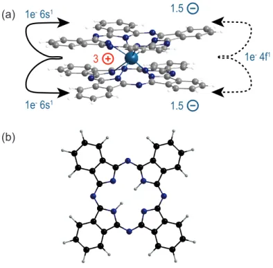
2molecule that consists of two phthalocyanine (Pc) rings with a neodymium ion in the center is shown in Fig. II.2 (a) to illustrate the double-decker structure of the molecule. The bare phthalocyanine molecule (H
2Pc) with the molecular formula C
32H
18N
8is illustrated in Fig. II.2 (b). It consists of four isoindole rings linked by four nitrogen atoms forming a molecule with a four-fold symmetry. The two chemical bonds to the nitrogen atoms in the center are satisfied by hydrogen atoms.
Figure II.2: (a) NdPc2
double-decker phthalocyanine molecule. The bonding of the molecule is mainly of electrostatic character. The central Nd atom transfers three electrons to the two phthalocyanine rings. (b) phthalocyanine molecule with two hydrogen atoms in the center. The molecule consists of four isoindole rings linked by nitrogen atoms. Atomic repre- sentation: hydrogen (white), carbon (grey), nitrogen (dark blue) and neodymium (blue).
3
1.5
1.5 1e
-6s
11e
-6s
11e
-4f
1(b) (a)
The electronic configuration of the neutral neodymium atom is [Xe]4f
46s
2. After bonding with the two hydrogen-free phthalocyanine rings three electrons are transferred from the central ion to the rings, namely the two 6s
2and one 4f -electron, indicated by the arrows in Fig. II.2 (a). Since each of the two rings would accept two electrons, one electron is shared by them. This results in a charge of 3e
+on the central ion and a net charge of 1.5e
−left on each of the rings. In consequence the bonding of the molecule is mainly of electrostatic nature and there is only a weak electronic coupling from one phthalocyanine via the central atom to the other ring. This hybridization [29] but also the repulsive negative charges on the two Pc rings lead to a relative rotation of 45
◦with respect to each other. As a consequence of the charge transfer the Nd atom will remain with three f −electrons in one spin-channel while the two Pc ligands will share the former Nd 4f -electron in the opposite
10
II.4 NdPc
2Double-Decker Molecule
spin-channel. It is known that in systems comprising atoms with high atomic number Z the spin-orbit coupling (SOC) strongly modifies the band structure. For this reason a calculation of the total magnetic moment of the molecule is only feasible by including SOC.
However, charge density calculations of the free NdPc
2molecule including SOC show that the energetic position of the states is barely influenced. This allows to neglect the SOC in the calculations for the adsorbed NdPc
2molecule in this study and has been done for the reason to reduce the anyway long computing times. As a result an information about the total magnetic moment cannot be given here. Nevertheless, the total spin moment is known and results to 2(
ps
Nd(s
Nd+ 1) −
ps
Pc(s
Pc+ 1)) µ
Bwith s
Nd= 3/2 on the Nd ion and s
Pc= 1/2 on the two organic ligands, respectively.
Different lanthanide double-decker molecules have been studied under the aspect of single molecular magnetism [4, 28], but the NdPc
2molecule was throughout neglected in these studies. The intramolecular bonding inside the NdPc
2is weak compared to those molecules comprising late lanthanide atoms with higher atomic number [30]. This leads to very low yields in the synthesis of the molecules. These low yields are the main reason why NdPc
2was not included in earlier studies and the interest focused on lanthanide atoms with higher occupied 4f -orbitals. So far TbPc
2and DyPc
2are already known to be SSM with long relaxation times and hysteretic behavior, when measured in bulk and diamagnetic diluted bulk samples. The high blocking temperatures of several tens of Kelvin [28, 31]
make them extremely interesting compared to transition metal complexes. The highest blocking temperatures reported for the latter are below 8 K [18]. As a consequence, the electronic properties of TbPc
2and DyPc
2adsorbed on different surfaces have been studied in the past by various of techniques. Vitali et al. [32] for example performed STM studies on the TbPc
2molecule adsorbed on Cu(111) indicating that the SMM character might be preserved despite strong substrate molecule interaction. The same behavior was observed by Stepanow et al. [33] by means of XMCD measurements on TbPc
2adsorbed on Cu(100), where the magnetic moment of the molecule is found to be of Ising type and aligns parallel or antiparallel to the surface normal. Kondo resonances were absent for TbPc
2, DyPc
2and YPc
2when studied as single molecules adsorbed on Au(111) [34, 35], whereas a Kondo resonance could be observed and manipulated for TbPc
2grown as islands on Au(111) [22]. More recently Schwöbel et al. reported about spin-polarized STM on TbPc
2single molecules adsorbed on the ferromagnetic surface cobalt on iridium [36]. As already mentioned above it was also shown that TbPc
2attached to carbon nanotubes can function as a molecular spin-valve device [15].
Besides the lack of experimental information regarding its molecular magnetism NdPc
2is a promising candidate for electronics with single molecular magnets from the theoretical
point of view. For spintronic applications it is important that the 4f -states that give rise
to the magnetic moment, lie energetically and spatially in a range accessible to transport
experiments. Compared to the prominent TbPc
2molecule, the 4f-electrons in NdPc
2lie
closer to the Fermi energy and can more easily be tuned by the molecular framework and
accessed in a transport experiment. A similar argument is valid for the spatial position of
the orbitals. Figure II.3 shows an excerpt of the periodic table of the elements for selected
atoms of the period of the lanthanides. The occupation of the 4f -orbitals is lower in the Nd
II Molecules in Spintronics
La
5760
Nd
4f4 6s265
Tb
4f9 6s266
Dy
4f10 6s2... ...
ionic radius
Figure II.3.: Excerpt of the periodic table of the elements for selected atoms of the lanthanide period.
atom compared to Tb and Dy, due to its lower atomic number Z leading to orbitals which are less localized around the nucleus. The increased spatial extend of the 4f-electrons in the NdPc
2molecules leads to lower binding energies and also geometrically favors the accessibility of the magnetic states in transport experiments.
By means of combined density functional theory and scanning tunneling microscopy investigations of the NdPc
2molecule on Cu(100) it will be confirmed in Chapter VI that the direct access to the 4f-states of the molecule is indeed possible.
12
CHAPTER III
Scanning Tunneling Microscopy
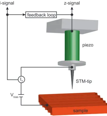
Scanning tunneling microscopy (STM) and spectroscopy (STS) are versatile tools to inves- tigate topographic, electronic, and magnetic properties of conducting surfaces down to the atomic scale. The working principle is based on the quantum mechanical tunneling effect of electrons tunneling through a gap between surface and probing tip.
As shown in Fig. III.1 an atomically sharp tip is approached to a conducting surface down to a distance of a few Å.
piezo
STM-tip
sample IT
feedback loop
I-signal z-signal
Vbias
Figure III.1: Schematic drawing of the working principle of a scan- ning tunneling microscope (STM).
An atomically sharp tip is ap- proached to a surface until a tun- neling current will occur due to the applied bias voltage. A piezo scan- ner moves the tip across the surface.
III Scanning Tunneling Microscopy
When applying a bias voltage, a tunneling current occurs and provides information about the surface. A scanner consisting of a cylindrical crystal of piezo-electric material moves the tip across the surface. Two pairs of electrodes sit on the outside of the piezo element, while the inner side is entirely covered by one electrode. Applying voltages to either one of the outer pairs of electrodes relative to the inner ones, depending on the polarity, will bend the piezo in the corresponding direction and the x and y movement is generated.
By applying a voltage between the inner and all four outer electrodes, the entire piezo will, depending on the voltage polarity, expand or contract in z-direction. While scanning across the surface the tunneling current I and the piezo motion ∆z are recorded. There are two different ways of imaging the surface. In both cases, the tip is stabilized at a certain bias voltage and tunneling current. In the constant height mode, the feedback loop of the STM is switched off and the height z stays constant while scanning along the surface. In the constant current mode the principle is different. The current I is kept at a constant value, while the feedback loop regulates the height z. Throughout this work, STM images recorded in the constant current mode will be presented.
In the following Sections, the theoretical background of the working principle of STM and STS with non-magnetic and magnetic tips will be introduced to provide the basis for the interpretation of the experimental data within this work.
III.1. The One Dimensional Tunneling Effect
Towards the understanding of the basic principle of scanning tunneling microscopy it is helpful to start with taking a closer look at the one dimensional quantum mechanical tunneling effect. Let us consider a finite potential barrier with the height V
0and thickness d and a particle that tends to cross this barrier as shown in Fig. III.2.
classical quantum mechanical
V0 E
0 d
V0 E
0 d
I II III
(a) (b)
Figure III.2.: (a) A classical particle with the energyE approaching an energy barrier of the heightV0, withV0> E will be reflected. (b) A quantum mechanical particle, described by a wave function Ψ with the an energy E < V0 will have a certain probability to penetrate or even cross (tunnel) through the barrier.
The analogues in scanning tunneling microscopy would be the vacuum gap between tip and sample and the electrons carrying the current. As shown in Fig. III.2 (a) in case the energy of the incoming classical particle is lower than V
0it will be reflected at the barrier. In the quantum mechanical picture the particle can be described as a wave function Ψ(z) and thus
14
III.1 The One Dimensional Tunneling Effect
has a certain probability to penetrate or even cross the energy barrier (see Fig. III.2 (b)).
This probability can be determined by solving the time independent Schrödinger equation.
− ~
22m
d
2dz
2+ V
0(z)
!
Ψ(z) = EΨ(z) (III.1)
for the three areas, in front of (I), inside (II) and behind (III) the barrier. The solution for area (I) and (III) in front of and behind the barrier are of the form of plane waves
Ψ
I(z) = Ae
ikz+ Be
−ikz(III.2)
Ψ
III(z) = Ce
ikz(III.3)
with k
2= 2mE/ ~
2. Whereas inside the barrier of the height V
0, the wave function will describe an exponential decay
Ψ
II(z) = De
κz+ Ee
−κz(III.4)
with κ
2= 2m(V
0− E)/ ~
2. For a first estimation of the tunneling current present in the experiment the ratio between transmitted |C|
2and incoming |A|
2fraction of the wave is vital, because it can directly be compared to the ratio of transmitted and incident current density and therefore describes the characteristic of the tunneling current. The transmission coefficient
T = |C|
2|A|
2(III.5)
can be calculated by determining the coefficients A, C, taking into account the requirement that the wave function and its derivative has to be uniformly continuous. Additionally considering a thick and high barrier (κd >> 1), which is reasonable for typical STM parameters leads to
T ≈ 16k
2κ
2(k
2+ κ
2)
2· e
−2κd. (III.6) This result is the basis for interpretations of the current in STM. It shows an exponential dependence on both, the thickness of the barrier d and the effective barrier height ( √
Φ
eff=
√ V
0− E). For reasonable parameters in STM experiments (Φ
eff= 4 eV, d = 5 Å) it has the consequence that the increase of the barrier thickness by ∆d = 1 Å leads to a decrease in tunneling current by one order of magnitude. This result directly exhibits the high sensitivity of the STM to small changes in the topography down to less than a tenth of an Å. Another conclusion which is already possible to be drawn on the basis of this result is the dominance of the first atom at the apex of the tip. Electrons tunneling out of this atom will mainly contribute to the signal, leading to, not only the very high vertical resolution, but also to an atomic resolution in the lateral directions.
By considering the one dimensional tunneling effect it is possible to get a first impression
III Scanning Tunneling Microscopy
of the basic mechanisms of the STM, but of course this image is over-simplified. Up to this point the structure of the electrodes was neglected although the atomic and electronic configurations of the two electrodes, namely tip and sample, have to be taken into account to derive a more realistic STM model.
III.2. Interpreting STM Images
To account for a more realistic description of the tunneling current a theory developed by Bardeen already twenty years before the invention of the STM is applied. Bardeen [37]
calculated a system consisting of two planar electrodes seperated by an insulating oxide layer by means of first order perturbation theory. Within this theory the two electrodes are considered to be weakly interacting systems and the current is calculated based on the overlap of the wave functions inside the barrier. In 1983 Tersoff and Hamann [38, 39]
adopted this theory to the system consisting of tip and sample seperated by a vacuum gap.
Under the assumption of small biases and low temperatures the tunneling current is given by
I = 2π
~ e
2V
Xµν
|M
µν|
2δ(E
µ− E
F)δ(E
ν− E
F). (III.7) Here, e and V are the electron charge and the applied bias voltage. The indices µ and ν denote tip and sample, respectively. The delta-functions account for elastic tunneling of the electrons that means that the energy of the electrons is conserved during the tunneling process. The basic challenge when trying to apply Eq. (III.7) is the determination of the tunneling matrix element M
µν. It describes the transition of the states Ψ
νof the sample before tunneling and of the states Ψ
µof the tip after the tunneling process. M
µνdepends on the energy levels and wave functions of sample and tip and can according to Bardeen be written as
M
µν= − − ~
22m
Z
d ~ S(Ψ
∗µ∇Ψ ~
ν− Ψ
ν∇Ψ ~
∗µ). (III.8) Information about the exact energy levels and wave functions can only be obtained, if detailed information about the structure of the electrodes can be provided. This is especially in the case of the tip not possible. The tip is fabricated in a relatively uncontrolled way, mainly ex-situ, and detailed information can only be achieved for example by means of field emission microscopy with high efforts. Additionally the tip apex undergoes various changes, again in an uncontrolled manner, while recording the data during the experiment itself. To avoid being forced to provide detailed information about the tip apex additional assumption were introduced by Tersoff and Hamann. They proposed the tip sample geometry shown in Fig. III.3 with the tip representing a perfect spherical shape at the apex with the curvature R and the distance d from the surface. The position of the tip is given by ~ r
0. This proposal seems reasonable, when taking into account that the first atom at the tip apex, due to the exponential dependence of the current on the distance, is mainly contributing to the signal.
16
III.2 Interpreting STM Images
Tip
Sample d
R r
0Figure III.3: Schematic drawing of the tip- sample geometry. The tip is approximated by a spherical shape with the radiusRat the apex [39].
Furthermore only tip wave functions of the form of s-waves are considered to be present in the tunneling process.
1These further assumptions leads to a determination of the tunneling matrix element and modify the tunneling current to
I ∝ V n
texp(2κR)
Xν
|Ψ
ν|
2δ(E
ν− E
F), (III.9) in which n
tis the constant density of states of the tip at the position r ~
0and at the Fermi level. Furthermore one can identify the second part of Eq. (III.9)
n
s( r ~
0, E
F) =
Xν
|Ψ
ν|
2δ(E
ν− E
F) (III.10) as the local density of states (LDOS) of the surface at the Fermi energy. Equations (III.9) and (III.10) demonstrate two main features of the theory introduced by Tersoff and Hamann. First of all the role of the tip is reduced to simply being a probe of the sample characteristics and its contributions to the energy dependence of the tunneling current are neglected. And second, the results of the in the introduction of this Chapter already mentioned constant-current imaging, in which the tip is scanned across the sur- face by regulating the distance to keep the current constant, can be interpreted as maps of contours of constant local density of states of the sample. In a first approximation, these LDOS images are considered to reflect the topography of the sample surface. This approximation holds as long as the geometrical structures dominate over the electronic structures. On the atomic scale, the LDOS images can not longer be considered to re- flect topographic features, but the orbital character of the electron wavefunctions. As a result, depressions instead of protrusions might appear in atomic resolution images at the
1This immediately opens up questions regarding magnetic tips for spin-polarized STM, in which the d-orbitals are carrying the magnetic information necessary to achieve signals based on the tunneling magnetoresistance.
III Scanning Tunneling Microscopy
positions of the atoms. STM is therefore widely and mainly used as a tool to investigate surface structures, which were before the invention not accessible with techniques like low energy electron diffraction or other tools, which are based on diffracted particle or electro-magnetic waves. Attention has to be paid when imaging surfaces with atomic resolution. The measured and calculated corrugations strongly differ. Chen [40] solved this discrepancy in the Tersoff-Hamann model with developing an extended theory, where he included tip orbitals of lower symmetry, e.g. d
2z. Furthermore the interpretation of adsorbates on surfaces or surface alloys has to be made with the knowledge that it is not the topography that is measured in STM, but contours of constant LDOS. Due to their different work functions, oxygen adsorbates on metallic surfaces for example appear as depressions on the surface although they are protrusions from the topographic point of view.
While it was in the beginning mainly used as a tool to investigate the surface structure, the sensitivity of STM to the local electronic density of states of the sample opens up the possibility to investigate the electronic properties including magnetic properties of surfaces and is now widely used in this research area. In the next Section it will be shown that STM is best suited to probe the local density of states for occupied, but also unoccupied states of the investigated sample.
III.3. Probing the Local Density of States
Scanning tunneling spectroscopy (STS) offers the possibility to investigate the LDOS structure of a sample with lateral atomic resolution. It will be shown in this Section that the differential conductivity of the sample dI/dV as a function of the applied bias voltage V provides the information about the density of states.
In the approximations made in the last Section, only vanishing bias voltages were included. Now the theory will be extended to account also for finite bias voltages. The result of the Tersoff-Hamann tunneling current in Eq. (III.7) is then modified to
I ∝
Z eV0
n
t( − eV )n
s()T (, eV )d, (III.11) in which the net current originates from a convolution of the densities of state of tip and sample over the energy interval eV . The transmission coefficient, similar to the one introduced in Eq. (III.5) accounts for the exponential bias voltage and energy dependence of the tunneling current.
For a better understanding, Fig. III.4 visualizes the content of Eq. (III.11) on the basis of one dimensional energy diagrams. Tip and sample are considered to exhibit different work functions Φ
tand Φ
sand the density of states of the tip is according to the approximations made in the model supposed to be constant. The magenta line represents the density of states of the sample. At high distance, as plotted in Fig. III.4 (a), the two systems do not interact with each other. By bringing the two electrodes in tunneling contact, electrons are tunneling in both directions until the combined system is in equilibrium, which means the Fermi levels are located at the same energy [Fig. III.4 (b)]. An applied bias voltage
18
III.3 Probing the Local Density of States
φ
tφ
sEVacuum
EFermi
Tip Sample
(a)
(d) (c)
(b)
φ
tφ
sEVacuum
EFermi
Tip Sample
φ
tφ
sEVacuum
EFermi Tip
Sample
φ
tφ
sEVacuum
EFermi
Tip Sample
Figure III.4.:Sketch of the energy diagrams for a tunneling system. The sample DOS is indicated as a magneta line, whereas the DOS of the tip is considered to be featureless (constant). (a) Tip and sample in high distance from each other: No interaction. (b) Tip and sample in tunneling contact. Electrons are tunneling until both Fermi levels are in equilibrium. (c) Positive bias voltage at the sample. Electrons are tunneling from the tip to the sample, which results in probing the unoccupied sample states. (d) Negative bias at the sample. Electrons are tunneling from the sample to the tip, which results in probing the occupied sample states (as in [41]).
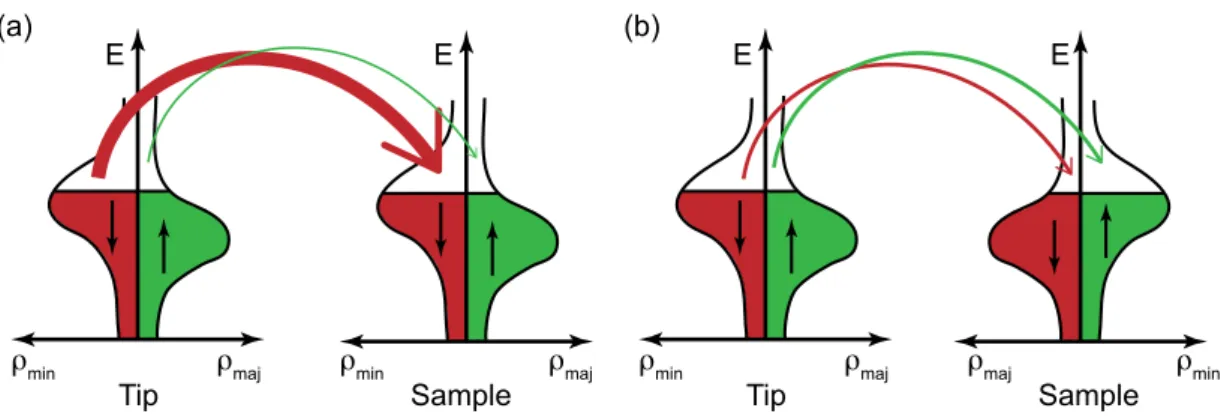
eV will shift the Fermi energy of one electrode with respect to the other and electrons tunnel from the negative to the positive electrode. In Fig. III.4 (c) a negative bias voltage is applied to the tip and electrons tunnel into unoccupied states of the sample, whereas in Fig. III.4 (d) electrons tunnel from occupied states of the negatively biased sample into the tip. The plotted arrows of different length represent the influence of the transmission coefficient T (, eV ). Electrons, which are located at the Fermi edge of the negatively biased electrode contribute most to the tunneling current. This can be intuitively understood by considering that they have to overcome the smallest energy barrier.
If we now in a further step differentiate Eq. (III.11) with respect to V dI
dV (V ) ∝ n
t(0)n
s(eV )T (eV ) +
Z eV0
n
t( − eV )n
s() dT (, eV )
dV d (III.12)
III Scanning Tunneling Microscopy
the correlation between the differential conductivity dI/dV and the LDOS of the sample becomes evident and can be attributed to the first term. The second term represents the influence of the bias voltage dependence of the transmission coefficient T (, eV ) and will appear in the STS experiment as a background on the signal. Different approaches to eliminate this background have been proposed [42, 43], but are not discussed and used in this work. The appearance of the transmission coefficent in the first term gives rise to an asymmetry in the dI/dV -signal, when changing the bias polarity. To explain this in detail, Figs. III.4 (c) and (d) are taken into account again. Probing the unoccupied states of the sample in STS is favored, because the electrons are tunneling from the Fermi edge of the tip, where the efficiency is highest (indicated by the long magenta arrow), into states at an energy E
F+ eV . In contrast to this, probing the occupied sample states means that electrons which lie deeper in energy and thus, exhibit lower tunneling efficiency, generate the tunneling signal. In view of these considerations, the assumption that the LDOS of the tip is flat becomes questionable. However, experimental results show that it is still applicable. Nevertheless it is also possible to eliminate the influence of the tip from the signal. This can be done by recording STS data at different sample positions, at which the LDOS of the sample is known to change, but the contribution of the LDOS of the tip is known to be unaltered. In conclusion the dI/dV -signal reveals the LDOS features of the sample and can be addressed in STS with the already mentioned high lateral atomic resolution intrinsic for STM.
The spectroscopic dI/dV -data shown in this work is obtained in the following experi- mental approach. A lock-in amplifier is used to add a small bias voltage modulation with a frequency higher than the cut-off frequency of the feedback loop (∆V = 20 mV, f = 2.7 kHz) to the applied bias voltage V . The resulting in-phase current modulations are detected by the same lock-in amplifier. The dI/dV -signal by this means detected is attributed to the LDOS of the sample. The spectroscopic data is displayed in two different ways, depending on the requested information. On the one hand the LDOS for a certain bias voltage V is plotted in a two dimensional image to show the spatial distribution of the contributing states of the LDOS at the energy E
F+ eV , which is then called a dI/dV -map. On the other hand the LDOS is plotted for a particular sample position as a function of the applied bias V to gain information about the energy dependency, which is called dI/dV -curve.
dI/dV -maps and constant current STM images are always recorded simultaneously. This offers the potential to directly compare spectroscopic properties to topographic features.
In case of the dI/dV -curves, the tip is moved to a selected sample position and stabilized at certain bias voltage-tunneling current values. During the acquisition of the spectra, the feedback loop is switched off and the bias voltage is swept within the chosen interval, while the lock-in amplifier detects the dI/dV -signal.
III.4. Spin-Polarized Tunneling Experiments
As already mentioned in the introduction to this Chapter, STM opens up the additional possibility to investigate not only the electronic, but also the related magnetic properties of surfaces. Therefore it is necessary to include the electron spin into the considerations so
20
III.4 Spin-Polarized Tunneling Experiments
far taken about the tunneling current. In 1989 Slonczewski [44] discussed the problem of electrons tunneling between two ferromagnetic electrodes and showed the cosine dependence of the tunneling current with respect to the relative alignment of the two magnetization directions of the electrodes (Θ). Under the assumption of vanishing bias voltages and electrons behaving like free electrons within the conduction band, the tunneling current can be expressed
I
sp= I
0[1 + P
1· P
2cos Θ], (III.13) with I
0being the spin-averaged current and P
i=
nni,↑−ni,↓i,↑+ni,↓
the spin-polarization, in which n
i↑/↓are the densities of states of the spin up and spin down electron states at the Fermi energy, respectively. The cosine-Θ dependence of the tunneling current is shown in Fig. III.5 observed for tunneling junctions consisting of Fe-Al
2O
3-Fe layers.
Figure III.5: Dependence of the magnetore- sistance on the relative angle between the two magnetization directions of a planar tunneling junction consisting of Fe-Al2O3-Fe [45].