D is se rt at io ns re ih e P hy si k - B an d 4 3 Johannes Kar ch
Photoelectric Phenomena in Graphene Induced by Terahertz Laser Radiation Christoph Johannes
Drexler
43
9 783868 451160
ISBN 978-3-86845-116-0
Christoph Johannes Dr exler
ISBN 978-3-86845-116-0
transport phenomena in graphene driven by the free-carrier absorp- tion of electromagnetic radiation are explored. It is demonstrated that in the presence of adatoms and/or a substrate, as well as in the vicinity of graphene edges the carriers exhibit a directed motion in response to the alternating electric field of the terahertz radiation.
Moreover, it is shown that these photoelectric phenomena can be giantly enhanced if graphene is deposited on a substrate with a neg- ative dielectric constant. Novel models of the photocurrent genera- tion are developed to describe the nonequilibrium processes in the purest two-dimensional material. The experiments together with the theoretical considerations give access to fundamental properties of graphene.
Christoph Johannes Drexler
Photoelectric Phenomena in Graphene Induced by Terahertz Laser Radiation
Herausgegeben vom Präsidium des Alumnivereins der Physikalischen Fakultät:
Klaus Richter, Andreas Schäfer, Werner Wegscheider, Dieter Weiss
Dissertationsreihe der Fakultät für Physik der Universität Regensburg, Band 43
Dissertation zur Erlangung des Doktorgrades der Naturwissenschaften (Dr. rer. nat.) der naturwissenschaftlichen Fakultät II - Physik der Universität Regensburg vorgelegt von
Christoph Johannes Drexler aus Hutthurm
im Mai 2014
Die Arbeit wurde von Prof. Dr. Sergey D. Ganichev angeleitet.
Das Promotionsgesuch wurde am 16.04.2014 eingereicht.
Prüfungsausschuss: Vorsitzender: Prof. Dr. Gunnar Bali 1. Gutachter: Prof. Dr. Sergey D. Ganichev 2. Gutachter: Prof. Dr. Josef Zweck weiterer Prüfer: Prof. Dr. Franz J. Giessibl
Christoph Johannes Drexler
Photoelectric Phenomena
in Graphene Induced by
Terahertz Laser Radiation
sind im Internet über http://dnb.ddb.de abrufbar.
1. Auflage 2014
© 2014 Universitätsverlag, Regensburg Leibnizstraße 13, 93055 Regensburg Konzeption: Thomas Geiger
Umschlagentwurf: Franz Stadler, Designcooperative Nittenau eG Layout: Christoph Johannes Drexler
Druck: Docupoint, Magdeburg ISBN: 978-3-86845-116-0
Alle Rechte vorbehalten. Ohne ausdrückliche Genehmigung des Verlags ist es nicht gestattet, dieses Buch oder Teile daraus auf fototechnischem oder elektronischem Weg zu vervielfältigen.
Weitere Informationen zum Verlagsprogramm erhalten Sie unter:
www.univerlag-regensburg.de
CONTENTS V
Contents
1 Introduction 1
2 Theoretical background 4
2.1 Crystallographic and electronic properties of graphene . . . 4
2.2 Optical transitions in graphene . . . 7
2.3 Second order photoelectric effects . . . 9
2.3.1 The photon drag effect . . . 10
2.3.2 The photogalvanic effect . . . 13
2.3.3 The magnetic field induced photogalvanic effect . . . 15
3 Experimental methods 19 3.1 Sources of high-power THz radiation . . . 19
3.1.1 Optically pumped molecular THz lasers . . . 20
3.1.2 The free electron laser FELIX . . . 22
3.2 Variation of the light’s polarization state . . . 24
3.2.1 The Stokes parameters . . . 24
3.2.2 Variation of the Stokes parameters by waveplates . . . . 26
3.2.3 Refractive index of crystal quartz . . . 28
3.2.4 Variation of the Stokes parameter by Fresnel rhomb . . . 30
3.3 Experimental Setups . . . 31
3.4 Graphene samples . . . 33
4 Magnetic quantum ratchet effect 38 4.1 THz photocurrents subjected to an in-plane magnetic field . . . 39
4.2 Microscopic model and theory . . . 45
4.3 Discussion . . . 50
5 Chiral edge currents 54
5.1 Edge current experiments . . . 54
5.2 Microscopic theory . . . 59
5.3 Discussion . . . 62
6 Reststrahl band assisted photocurrents 65 6.1 Photocurrent experiments . . . 65
6.2 Phenomenological analysis . . . 71
6.3 Fresnel analysis of the local electric fields . . . 73
6.4 Discussion . . . 77
7 Conclusion 80 8 Appendix 82 8.1 Helicity sensitive detection by field effect transistors . . . 82
8.1.1 Dyakonov-Shur model of broadband THz detection . . . 83
8.1.2 Sample and Setup . . . 85
8.1.3 Experimental Results . . . 87
8.1.4 Theory and Discussion . . . 91
8.1.5 Conclusion . . . 96
References 96
LIST OF FIGURES VII
List of Figures
1 Crystallographic structure in (a) real and (b) momentum space;
(c) band structure of graphene. . . 5 2 Optical transitions in graphene. . . 8 3 Photon drag effect for (a) parabolic and (b) linear dispersion. . 11 4 Geometry (a) and contributions to the (b) linear and (c) circular
photon drag effect. . . 12 5 Geometry (a) and contributions to the (b) linear and (c) circular
photogalvanic effect. . . 14 6 Microscopic model of the photogalvanic effect for (a),(b) parabolic
and (c) linear dispersion. . . 15 7 Model of the MPGE for (a) spin-related and (b) orbital mecha-
nisms. . . 16 8 (a) Principle of a molecular THz laser; (b) laser lines of the
available molecular THz lasers. . . 20 9 Schemes of (a) pulsed and (b) cw optically pumped molecular
THz lasers. . . 21 10 Scheme of a free electron laser. . . 22 11 Outline and dimensions of the free electron laser FELIX. . . 23 12 Set of vectors describing the (a) second, (b) third and (c) fourth
Stokes parameter; (d) Poincar´e sphere . . . 25 13 (a) Scheme of a λ/2 plate; (b) final polarization states. . . 26 14 (a) Scheme of a λ/4 plate; (b) final elliptical polarization states. 27 15 (a) Geometry for transmission experiments of quartz plates; (b)
resulting transmission spectra. . . 28 16 Spectral dependence of ∆n. . . 29 17 (a) Principle of a quarter wave Fresnel rhomb; (b) resulting
polarization states. . . 30
18 (a) Setup of the pulsed THz laser; (b) temporal shape of an excitation pulse; (c) spatial beam profile. . . 31 19 (a) Beam stage at FELIX; (b) pulse shape of FELIX. . . 32 20 (a) Layer profile of epitaxial graphene; (b) picture of sample Epi-
2 with bonding scheme; (c) dimensions and contact geometry of the samples. . . 34 21 (a) Layer profile of CVD-grown graphene; (b) pictures of sample
CVD-2. . . 36 22 Perpendicular photocurrent density jx(By) measured in sample
Epi-1. . . 39 23 Perpendicular photocurrent density jx(α) measured in sample
Epi-1 at By =±7 T. . . 40 24 Temperature dependence of the polarization dependent (j1) and
- independent (j2) photocurrent density measured in sample Epi-1 for |By|= 7 Tesla. . . 41 25 Summary of (a) experimental data and (b) temperature depen-
dence of carrier density n and mobility µ of sample Epi-2. . . . 42 26 Perpendicular photocurrent densityjx(By) measured in samples
Epi-1,2,3,6 and CVD-1. . . 43 27 Parallel photocurrent density jy(By) measured in response to
circularly polarized radiation. . . 44 28 Microscopic model of the magnetic quantum ratchet effect. . . . 46 29 Edge photocurrent J(ϕ) measured in sample Epi-5. . . 55 30 Circular edge photocurrentJA measured in sample Epi-5 under
variation of the laser spot position. . . 56 31 Circular edge photocurrent JA measured in sample CVD-2 un-
der variation of the laser spot position. . . 58 32 Vortex of the circular edge photocurrentJAmeasured in sample
(a) Epi-5 and (b) Epi-2. . . 59 33 Microscopic process activating the edge current generation. . . . 60
LIST OF FIGURES IX 34 Frequency- and ωτ- dependence ofJAfor sample Epi-2 and Epi-5. 62 35 Reflection spectra of silicon-carbide and graphene. . . 66 36 Linear transverse photocurrent jyL measured in sample Epi-5. . . 67 37 Linear longitudinal photocurrent jxL measured in sample Epi-5. . 68 38 (a) Transverse photocurrent jyL measured in sample Epi-5 in
response to elliptically polarized radiation; (b),(c) polarization dependencies at different photon energies. . . 69 39 Circular transverse photocurrent jyC measured in sample Epi-5. . 70 40 (a) Interference of local electric fields; (b)-(d) Calculated spec-
tral dependence of the linear and circular photocurrents. . . 74 41 Comparison of (a) experimental data and (b) theory of linear
and circular transverse photocurrent. . . 78 42 Schematic illustration of a FET operating in detection mode. . . 83 43 Transfer characteristic and dimension of a GaAs/AlGaAs high
electron mobility transistor. . . 86 44 Setup of the cw methanol laser. . . 87 45 (a) Gate bias dependence of the photovoltage USD for various
frequencies; (b) Experimental geometry; (c) transfer character- istic of the GaAs/AlGaAs-HEMT. . . 88 46 Photovoltage USD as a function of the azimuth angleα for var-
ious frequencies and gate voltages. . . 89 47 (a) Photoresponse USD measured for right- and left-handed cir-
cularly polarized radiation; (b) Helicity dependence of the pho- tovoltage. . . 90 48 (a) Experimental results and (b) calculated photovoltage USD
for the effective two-antenna model and a short channel. . . 94
List of Tables
1 Carrier density n, mobility µ, and Fermi energy EF of various epitaxial graphene samples at 4.2 K and room temperature. . . 35
1
1 Introduction
With the realization of graphene [1], the first truly two-dimensional crystal of carbon atoms, A. K. Geim and K. S. Novoselov launched an avalanche of ac- tivities in science and technology leading to the nobel-prize in 2010. One of the reasons for the immense interest in graphene is the linear coupling between the charge carrier energy and momentum [2]. Resulting from its crystallographic structure, the energy dispersion of graphene resembles that of massless re- lativistic particles described by the Dirac equation [3]. Consequently, many unusual features appear in graphene, e. g. an extraordinary high electron mo- bility making graphene valuable for studies of phase coherent phenomena [4–7], a zero energy Landau level resulting in a half-integer quantum Hall effect which is unique for monolayer graphene [8, 9], a two-state degree of freedom due to the presence of two equivalent valleys which was suggested to be used in val- leytronics [10], Klein tunneling [11–14], etc. (for review see e. g. Refs. [15–17]).
These and many other phenomena result in a huge amount of potential ap- plications [18], but on the way out of the labs straight into mass production and industrial applications, plenty of room for research and investigations on graphene is still given.
Most of the peculiarities listed above manifest in transport phenomena which are linear in the electric field and in the focus of research. In contrast, the transport phenomena which are nonlinear in the electric field are much less studied in graphene. In general, these effects result from the redistribution of charge carriers in the momentum and energy space, which were driven out of equilibrium by an alternating electric field provided, for instance, by external radiation. The radiation may cause bothac and dc current flows whose mag- nitudes are nonlinear functions of the field amplitude. Most of these effects are not peculiar for graphene and have been observed also in ordinary semi- conductor systems, such as e. g. conventional two - and three - dimensional semiconductors [19, 20] as well as carbon based systems like carbon nanotubes and carbon films (for review see, [21]), before.
Considering graphene, the nonlinear transport phenomena which arise in re- sponse to an optical high frequency (HF) electric field have attracted attention just recently. The basic difference is that the effects are strongly enhanced in
graphene compared to their ordinary counterparts in semiconductors, basically due to the high electron velocity and the linear dispersion in graphene. More- over, the microscopic mechanisms of these phenomena can be quite different in graphene. Among them can be found e. g., second - and third harmonic generation [22–24], frequency mixing [25], time-resolved photocurrents [26, 27]
as well as the photon drag - and the photogalvanic effect [28, 29] (for review see [30]). The two latter effects result in dc currents being proportional to the squared amplitude of the ac electric field of terahertz (THz) laser radia- tion. The THz radiation induced photocurrents have proven to be a powerful tool to study nonequilibrium optical and electronic processes in semiconduc- tors and provide information about their fundamental properties (for review see [19, 20]).
The main part of this thesis is aimed to the investigation of the nonlinear HF photoelectric phenomena in graphene resulting in a dc photocurrent. One of these phenomena is the magnetic quantum ratchet effect. Ratchets are sys- tems which exhibit, due to their built-in asymmetry, a directed motion when they are driven out of equilibrium by an alternating force. Examples have been observed in various scientific fields (for review see [31, 32]). In graphene, being almost perfectly two-dimensional and highly symmetric, any ratchet me- chanism is expected to be absent. However, it is demonstrated that when the symmetry is reduced by e. g., a substrate and/or adatoms, the Dirac electrons moving in an in-plane magnetic field drive a ratchet current. A shift of the electron orbitals leads to asymmetric carrier scattering for counter-propagating electrons. Hence, the periodic driving from THz radiation results in a directed ratchet current which indicates that orbital effects appear even in this purest possible two-dimensional system and gives access to the structure inversion asymmetry (SIA) in graphene.
In addition to the magnetic field induced currents, the chiral edge photocur- rents induced in the vicinity of the edges of graphene are demonstrated. It is shown that the second order correction of the electric field results in a directed current restricted to a narrow channel close to the sample’s edge. The investi- gations give direct access to the edge transport properties of graphene which are usually masked by the bulk transport properties.
Finally, the enhancement of the nonlinear photoelectric phenomena in gra-
3 phene within the spectral region of the reststrahl band of the substrate is demonstrated. The reststrahl band is characterized by a negative dielectric constant and almost perfect reflectivity. The strong modification of the local electric fields, acting on the carriers in graphene, due to the reflection at the substrate lead to anomalous spectral dependencies of the photocurrents which are amplified/ suppressed depending on the polarization state of the radiation.
The modifications are described by a macroscopic Fresnel formalism what is remarkable since the studied epitaxial graphene samples are situated within atomic distances from the substrate.
In addition to the nonlinear photoelectric phenomena in graphene, the helicity sensitive detection of THz radiation by field effect transistors is demonstrated.
The mechanism behind the generation of the dc response in a FET is quite different compared to that of the phenomena studied in graphene. However, the photosignals are several orders of magnitude higher. Consequently, the FETs show great potential as sensitive THz detectors. While the response to linearly polarized radiation has been addressed recently, the response which is sensitive to the helicity of circularly polarized THz radiation has not been observed so far.
The dissertation is organized as follows: In Chapter 2, the theoretical back- ground which is necessary to study the nonlinear photoelectric phenomena in graphene is presented. The experimental methods are discussed in Chap- ter 3, containing an overview of the used sources of THz radiation as well as a description of the radiation’s polarization state and methods for its variation.
This is followed by the experimental setups and an overview of the investigated samples. Chapter 4 is devoted to the investigation of the magnetic quantum ratchet effect in graphene. A detailed experimental investigation is presented which is followed by a microscopic model and theory. In Chapter 5, the ex- perimental observation of the chiral edge photocurrents is presented which is followed by a semiclassical theory. The reststrahl band assisted photocurrents are presented in Chapter 6. The experimental findings are discussed in terms of the phenomenological theory and qualitatively reproduced within a macros- copic Fresnel formalism. Finally, in the appendix of the thesis the helicity sensitive THz detection by field effect transistors is discussed.
2 Theoretical background
In the first chapter, the theoretical background of nonlinear HF photoelec- tric phenomena in graphene is presented. It starts with an introduction to the crystallographic and electronic properties of graphene, the monoatomic layer of carbon atoms. Therefore, the crystal structure resulting in a linear rather than a parabolic band structure is addressed. Moreover, the differ- ences between the relativistic carriers in graphene and that in conventional two-dimensional (2D) electron or hole systems in semiconductor nanostruc- tures are summarized. Subsequently, different optical absorption mechanism in graphene are presented.
Afterwards, the nonlinear HF photoelectric phenomena are introduced. First, a general description of the nonlinear response of the current density to anac electric field oscillating with a frequency lying in the THz range is given. Sub- sequently, the focus is shifted towards the effects which are proportional to the squared amplitude of the radiation’s electric field, i.e. the dc photocurrents.
Three classes of phenomena are presented to give an idea how anac THz field can be converted into a directeddc current.
2.1 Crystallographic and electronic properties of gra- phene
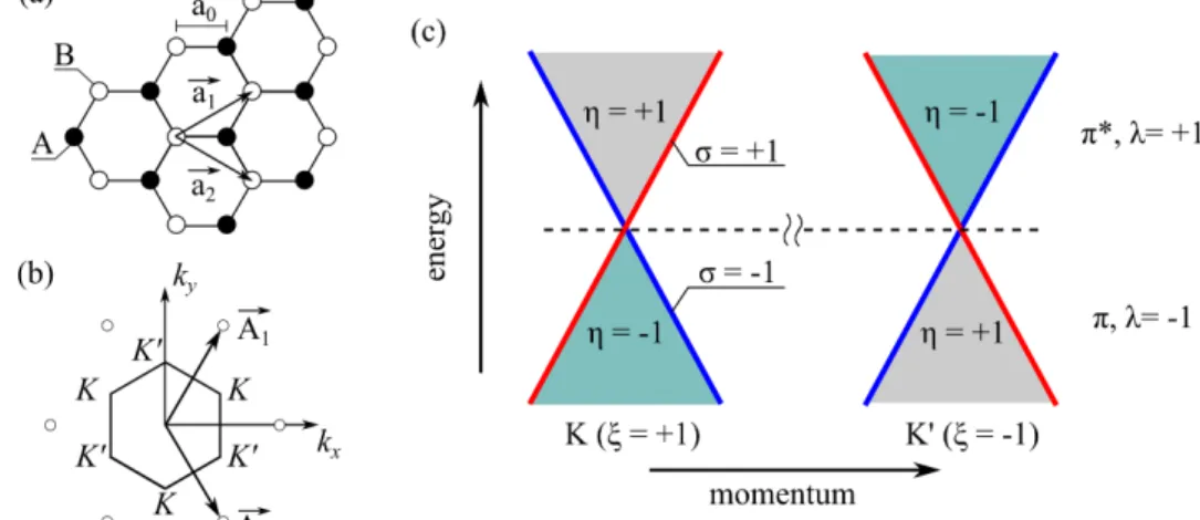
Discovered as the first perfect 2D crystal [1], graphene owes it’s fundamental physical properties to its crystal structure. Due to sp2 hybridization each carbon atom forms σ bondings to three nearest neighbor atoms with relative angles of 120◦. The remainingpz (π) orbital is decoupled from the hybridized orbitals and is delocalized over the entire crystal. As a result, the atoms assemble in the peculiar honeycomb lattice structure. The graphene lattice can be described by a unit cell with two atoms A and B, each of them arranged periodically in a triangular sublattice (Fig. 1 (a)). In real space, the primitive vectors are given by a~1 = a2 3,√
3
and a~2 = a2 3,−√ 3
where a = 0.142 nm is the distance between nearest neighbors. In the reciprocal space the corresponding primitive vectorsA~1 and A~2 are determined from the condition ai·Aj = 2πδij leading to A~1 = 2π3a 1,√
3
and A~2 = 2π3a 1,−√ 3
. As a result,
2.1 Crystallographic and electronic properties of graphene 5 the first Brillouin zone of the honeycomb lattice is a honeycomb lattice as well.
A closer look onto the six points at the corners of the Brillouin zone reveals that two different groups of equivalent points are present which are denoted as K and K’. While points belonging to one group can be interconnected with the reciprocal lattice vectors, these vectors cannot connect the K with the K’
points (see Fig. 1 (b)).
Figure 1: Honeycomb lattice of sp2hybridized carbon atoms in real (a) and momentum (b) space. (c) shows band structure of graphene close to the Dirac cones at K and K’ with associated lattice pseudospins σ and chiralitiesη (grey and green cones).
Although graphene is experimentally available only for almost one decade, it has been theoretically investigated for the first time more than half a century ago [2]. P. R. Wallace derived the relation between energyE and momentum k of a carbon monolayer within a tight binding approximation up to second order nearest-neighbor hopping:
Eλ=±1 ≈3t′+λ~vF|k| −
9t′a2
4 +λ3ta2
8 sin(3θk)
|k|2. (1) Herein,λ is the band index where ”+1” stands for the conduction band (anti- bonding, π∗- orbitals) and ”-1” for the valence band (bonding, π- orbitals), t is the nearest neighbor hopping amplitude (hopping between A and B sublat- tice), t′ describes next nearest neighbor hopping (hopping within either A or B sublattice), vF = 3ta/2 is the Fermi velocity and θk = arctan−1[kx/ky] is
the angle in the momentum space. In the vicinity of K- and K’-points Eq. (1) can be rewritten in the form
Ek,ξ=±1λ =λ~vF|k|, (2)
by neglecting next nearest neighbor hopping. This relation is commonly used to describe graphene’s band structure and reveals a linear connection of energy and momentum which was confirmed experimentally, for instance in Ref. [33].
The band dispersion is equal to that of ultrarelativistic particles with zero rest massm0, usually described by the Dirac equation instead of Schr¨odinger’s equation [3]. Therefore, close to the K- and K’-points the carriers in graphene behave like relativistic particles with single-particle Fermi velocities in the order of 108 cm/s [16] and are often denoted ”Dirac fermions”, whereas K and K’ are often referred to as the ”Dirac points”. Moreover, it follows from Eq. (2) that at the K- and K’-points where |k| = 0, conduction and valence bands touch each other identifying graphene as a zero band-gap semiconductor or a semimetal. The band structure of graphene reveals several peculiarities which can be explained in terms of an effective Hamiltonian for spinless graphene carriers near the Dirac points [17]:
Hef f,ξ=±1k =ξ~vF(kxσx+ξkyσy). (3)
Herein,σx,yare the Pauli matrices describing the ”sublattice” pseudospin quan- tum number σ = ±1. In addition, ξ describes the two equivalent valleys at the K- (ξ = +1) and K’-points (ξ = −1) which are called the ”Dirac cones”.
Their presence reveals a two-fold valley degeneracy for graphene which is of- ten referred to as the ”valley” pseudospin. Although both pseudospins can be represented by Pauli matrices, they are independent of the electron spin.
The peculiar lattice and band structure of graphene leads to several new pheno- mena. For instance, the presence of the sublattice pseudospin leads to a novel chirality quantum number ηk, also called helicity, which is described by the projection of the pseudospin onto the direction of motion of the carriers [17]:
ηk = k·σ
|k| . (4)
Thus, the chirality quantum number isη= +1 (-1) for particles within the con- duction (valence) band (see different colors in Fig. 1 (c)) at the K-point, and
2.2 Optical transitions in graphene 7 vice versa at the K’-point. In elastic scattering processes the chirality quantum number is conserved. This gives rise to the absence of intervalley scattering in pristine graphene and is the origin of Klein tunneling according to which a massless Dirac particle is fully transmitted, under normal incidence, through a high electrostatic barrier without being reflected [11–14]. Many other pe- culiar phenomena have been reported so far and are nicely reviewed, e. g. in Refs. [15–17].
To summarize, graphene’s electronic properties differ significantly from that of conventional 2D semiconductor heterostructures. First, graphene is a gap-less semiconductor. While in common semiconductors 2D electrons or holes can only be studied in separately doped structures, in graphene both regions can be achieved within the same system by varying the Fermi level, e. g. by gating.
Second, graphene particles are chiral, that of common semiconductor systems are not. This opens the door to completely different effects and physics. Third, graphene shows a linear dispersion relation rather than a quadratic one like con- ventional 2D semiconductors do. This gives rise to a vanishing effective mass of particles in graphene whereas carriers in conventional systems exhibit usually a finite effective mass. Finally, the carrier confinement in graphene is perfectly two-dimensional since the layer is exactly one atom thick (≈ 0.345 nm). By contrast, the confinement in heterostructures or quantum wells is usually in the order of a few nanometers or more and therefore, depending on the number of occupied subbands, not perfectly two-dimensional.
2.2 Optical transitions in graphene
Besides the peculiar electronic properties, graphene shows also interesting opti- cal properties. Most outstanding is the almost frequency independent absorp- tion of intrinsic graphene which assumesπα≈2.3% in vacuum [34]. Therein, α is the fine-structure constant. However, for reasons shown below, the gra- phene samples investigated in this thesis are typically ofn- type doping with Fermi energies of several hundreds of meV. In these structures, the condition EFτ /~ >> 1 is valid and electrons can be considered as free carriers. Conse- quently, depending on the Fermi - and the photon energy, additional absorption mechanisms become important.
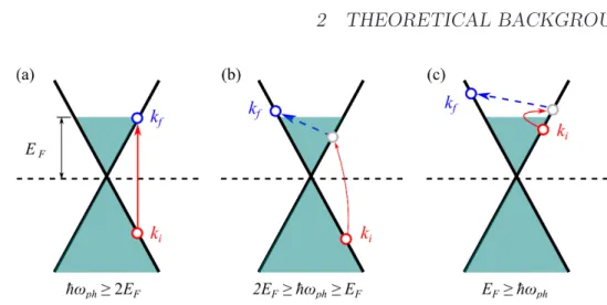
Figure 2: Scheme of possible transitions in graphene forEF > 0: (a) direct interband transition, (b) indirect interband transition, (c) indi- rect intraband transition. Red arrows indicate electron-photon interac- tion, Blue dashed arrows represent electron scattering by impurities or phonons. Initial (Final) states are shown by red (blue) circles. Grey circles indicate virtual states.
In Fig. 2, the three different absorption regimes relevant for the conditions mentioned above are illustrated:
• direct interband transitions:
In the case when the photon energy exceeds twice the Fermi energy,
~ωph ≥2EF (Fig. 2 (a)), the absorption of a photon results in the exci- tation of a final electronic state kf.
• indirect interband transitions:
If the condition 2EF ≥~ωph ≥EF is valid (Fig. 2 (b)), direct interband transitions are not possible. Assisted by electron scattering on phonons or impurities, an electronic state in the conduction band can be excited as far as energy- and momentum conservation are fulfilled.
• indirect intraband transitions:
If the photon energy is lower than the Fermi energy (Fig. 2 (c)), the Drude-like free carrier absorption leads to indirect intraband transitions via intermediate states which are accompanied by electron scattering on phonons or impurities.
2.3 Second order photoelectric effects 9 As it turns out, at THz frequencies (~ωph≈10 meV), the latter regime becomes dominant. In this case, the ac or high frequency conductivity, describing the electric current in response to the radiation’s electric field, is given by:
σ(ω) = σ0
1 +iωτ
1 + (ωτ)2, (5)
what is known as the Drude-Lorentz law of high-frequency conductivity [35].
The imaginary part of the conductivity indicates that the carriers lag behind the electric field of the radiation since they need roughly the timeτ to accel- erate in response to the change of the alternating field. This phenomenon is also called retardation and increases with higher angular frequencies ω.
2.3 Second order photoelectric effects
The aim of the thesis is to studydcphotocurrents which result from the redis- tribution of a carrier ensemble in momentum space which was excited out of equilibrium by the absorption of THz radiation. In order to describedccurrents in response to an opticalac electric field it is convenient to use the coordinate and time-dependent electric current density j(r, t) =σ·E(r, t) and expand it in series of powers of the electric field E(r, t) = E(ω,q) exp (i(−ωt+qr)) + E∗(ω,q) exp (i(ωt−qr)) [30]:
j(r, t) =h
σ(1)αβEβ(ω,q)e−iωt+iqr+c.c.i +h
σ(2αβγ′)Eβ(ω,q)Eγ(ω,q)e−2iωt+2iqr+c.c.i +h
σ(2)αβγEβ(ω,q)Eγ∗(ω,q) +...i .
(6)
Herein, q is the photon wavevector, Greek subscripts represent Cartesian co- ordinates and c.c. stands for the complex conjugate. The first term in Eq. (6) describes the response which is linear in the electric field. The second term oscillates with 2ω and is known as the second harmonic generation. Effects related to the first two terms are out of scope of this thesis. In the focus are processes characterized by the second order nonlinear conductivityσ(2)αβγ. These processes result in a static response which shows a quadratic dependence on the radiation’s electric fieldE(r, t), in other terms a linear dependence on the
radiation’s intensityI ∝ |E(r,t)|2.
Without any knowledge of the microscopic details, it is convenient to use sym- metry arguments in order to characterize these effects upon variation of the radiation’s polarization and its angle of incidence. Considering a spatial inver- sion r → −r, the vector of the electric current density j(r, t) changes its sign while the quadratic combinationEβ(ω,q)Eγ∗(ω,q) in the third term of Eq. (6) does not. Hence, second order effects are only allowed either if the second- order conductivity σαβγ(2) (ω,q) changes its sign upon spatial inversion or if the spatial inversion is not compatible with the symmetry of the system. The first condition is achieved if the conductivity tensor has components coupling to the photon wavevector q which changes its sign upon spatial inversion. The latter one is allowed if the studied system suffers a lack of inversion symmetry.
Thus, the electric current density can be decomposed in two parts:
j(r, t) =σαβγ(2) (ω,q)Eβ(ω,q)Eγ∗(ω,q), (7)
=h
σ(2)αβγ(ω,0) + Φαβγµ(ω)qµ
iEβ(ω,q)Eγ∗(ω,q), (8)
The first term contains all contributions toσ(2)αβγ(ω,0) which are independent of the photon wavevector and describe the class of photogalvanic effects (PGE).
The contributions which emerge due to the linear coupling to the photon wavevector are described by the fourth rank tensor Φαβγµ(ω). Such effects belong to the class of the photon drag effect (PDE). Both effects are discussed in the following.
2.3.1 The photon drag effect
The idea of a dc current flow in response to the photon momentum (second term of Eq. (8)), in other terms the radiation pressure, was introduced in 1935 [36]. In 1954, the effect was studied in the classical frequency limit of photon energies which are small compared to the typical electron energy [37].
In that work, thedccurrent is described as the result of the joint action of the radiation’s electric and magnetic field and was denoted as theacdynamic Hall effect. The effect was studied in epitaxial graphene in Ref. [28] as the classical limit of the PDE for photon energies which are small compared to the Fermi
2.3 Second order photoelectric effects 11 energy (Eph << EF) in doped graphene samples. It was also shown that in the quantum limit of the drag current (Eph ≤EF) the dynamic Hall contribution
∝EβBγ∗, describing the coupling of the complex amplitudes of E and B, can be written in the form of a photon drag effect ∝qδEβEγ∗. The PDE was also observed in response to direct interband transitions [38], but this mechanism is out of scope of the present discussion.
(b)
ki kf
ki kf
ki kf
ki
kf
(a)
f1 f2
E
qx jx e1
kx
Figure 3: (a) Model of the PDE for a parabolic band-structure caused by Drude absorption, (b) schematic illustration of processes responsible for the drag current in doped graphene samples: red arrows denote electron-photon interaction, blue arrows stand for electron scattering by phonons/impurites.
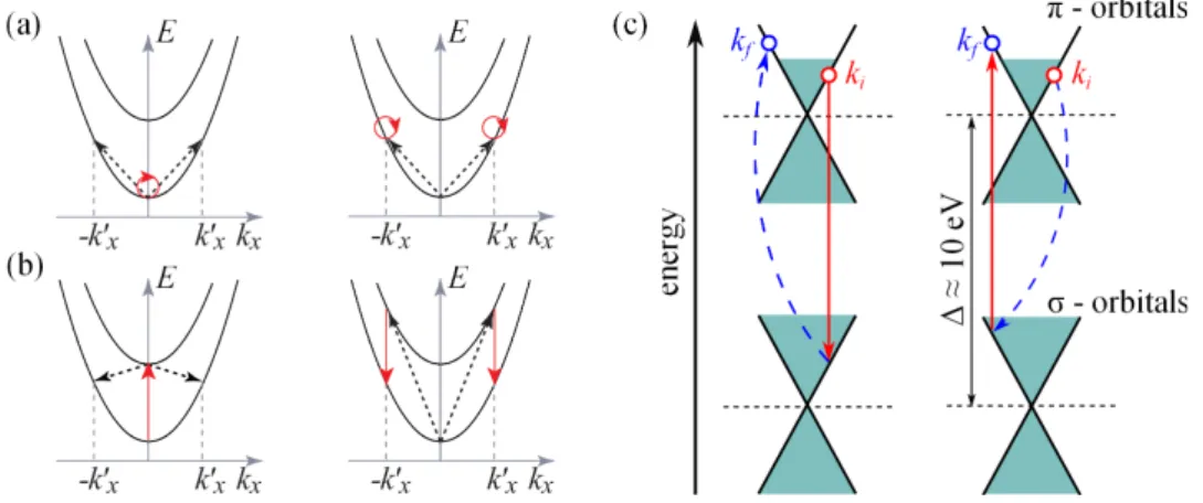
A simplified scheme of the photon drag effect for a parabolic band structure and in response to Drude absorption is depicted in Fig. 3 (a). By taking into account the photon wavevector qph the excitation of an initial state (k
= 0) into final electronic states f1 and f2 is done via a virtual state ν with k 6= 0. The lack of momentum between virtual and final states is provided by scattering processes, e. g. by acoustic phonons. The energy of acoustic phonons can be neglected in the THz range because it is small compared to the corresponding photon energies Eph. Scattering events providing q1 and q2 appear with nonequal probabilities (see arrows of different thicknesses in Fig. 3 (a)). As a consequence, f1 and f2 get asymmetrically excited leading to an imbalance of carriers ink-space, in other terms to a directeddc current jx. Although this model is oversimplified it describes the underlying processes
behind the photon drag effect. In graphene, the PDE was studied within the quantum frequency range (Eph≤EF) in Ref. [29] for doped systems where the intraband absorption process is more complex. A scheme for possible pathways is depicted in Fig. 3 (b). The Drude absorption appears via electron-photon interaction (red arrows) and is followed by an additional electron scattering process (blue dashed arrows) since energy and momentum conservation laws are violated otherwise.
(a) (b) (c)
jx
jy ħω
jx jy
qx
ħω, q
E ( )
jy qx
ħω, q
E ( ) Pcircez
Figure 4: (a) experimental geometry of Eqs. (9) and (10); contribu- tions to jx and jy due to the linear (b) and circular (c) photon drag effects.
Phenomenologically, the symmetry analysis of Eq. (8), considering the D6h
symmetry point group representative for a pristine graphene layer without substrate reveals the current density for the photon drag current in response to elliptically polarized radiation [29]:
jx =T1qx
|Ex|2+|Ey|2 2
+T2qx
|Ex|2− |Ey|2 2
, (9)
jy =T2qx
ExEy∗+Ex∗Ey
2
−T˜1qxPcirceˆz(|Ex|2+|Ey|2). (10) Therein, (xy) is chosen as the plane of the graphene sheet and (xz) as the plane of incidence (see Fig. 4 (a)). It follows that the PDE requires oblique incidence of radiation, since qx vanishes for normal incidence. The linear photon drag current, described by T1 and T2 is present in both longitudinal (|| x) and transverse (|| y) directions. By contrast, the circular photon drag current being sensitive to the degree of circular polarization, Pcirc, and described by T˜1 is present only in transverse direction. The equations reflect the main features of the PDE: i) the current is coupled to the presence of an in-plane component of the photon wavevector qx and ii) the current is proportional to the squared amplitude of the radiation’s electric field E(r, t). Here it’s worth
2.3 Second order photoelectric effects 13 mentioning that any reduction of the symmetry does not change the general form of Eqs. (9) and (10).
2.3.2 The photogalvanic effect
While the PDE is related to the linear coupling of the photon wavevector to the symmetric part of the conductivity tensor in Eq. (8), also its asymme- tric part, σ(2)αβγ(ω,q = 0), may lead to the generation of a dc current. The related phenomena are the so called photogalvanic effects and are possible in noncentrosymmetric media only, such as e. g. graphene on a substrate, and are forbidden in perfectly symmetric systems like pristine graphene. Similarly to the PDE, the PGE was observed as early as the 1950’s, but was correctly identified as a new phenomena in 1974 [39]. Up to now, linear and circular PGE have been studied in e. g., bulk materials, Si-MOSFETs and quantum wells (for review see [19, 20]). Phenomenologically, for the C6v point group symmetry, which is representative for graphene on a substrate, and the same experimental geometry as considered above the current density can be written as [29]:
jx =χl
ExEz∗+Ex∗Ez
2 , (11)
jy =χl
EyEz∗+Ey∗Ez
2 +χcPcirceˆx(|Ex|2+|Ey|2). (12) Therein, χl (χc) describes the linear (circular) PGE. It turns out that the po- larization dependence is similar to that of the PDE. The basic difference is that the PGE requires a z - component of the radiation’s electric field instead of an in-plane wavevector component, restricting it’s observation to oblique incidence as well. As a consequence, both effects are hard to distinguish from each other concerning their dependencies on the radiation’s polarization state and the angle of incidence. The observation of the photogalvanic effect in gra- phene is most likely under conditions where the photon drag effect is reduced, e. g. at high radiation frequencies [29].
Microscopically, in the quantum frequency range thedc current driven by the PGE results from a quantum interference of two processes: i) Drude-like in- direct optical transitions, described by the transition matrix element Mk(1)
f,ki,
(a) (b) (c)
jx jy ħω
E(ω) ħω
jy Ez
E(ω) ħω
jx jy Ez
Figure 5: (a) experimental geometry of Eq. (11) and (12); contribu- tions to jx and jy due to the linear (b) and circular (c) photogalvanic effects.
which are linear in k and ii) indirect intraband transitions with intermediate states in distant bands represented by Mk(2)
f,ki, which are almost independent of k. The scheme of possible pathways of transitions is shown in Fig. 6 for parabolic bands of a Si-MOSFET (a) and the linear dispersion of graphene (b). A transition from an initial ki to a final kf electronic state is possible only due to the interference of both effects. The total transition rate is given by [40]:
Wkf,ki ∝ |Mk(1)f,ki +Mk(2)f,ki|2 =|Mk(1)f,ki|2+|Mk(2)f,ki|2+Re[Mk(1)f,kiMk(2)f,ki].
(13) Herein, only the last term,Re[Mk(1)f,kiMk(2)f,ki], which describes the quantum in- terference, is linear ink. The first term is an even function of the wave vector, whereas the second term is independent of k. Hence, only the interference of both processes results in an imbalance of the carrier distribution in thek-space and thus, in adc photocurrent.
Considering graphene, the distant energy bands necessary for the interference are formed from σ-orbitals. It was shown that σ-orbitals form a deep valence band which is separated from theπ-orbital valence band by roughly 10 eV [41].
Consequently, the PGE in graphene arises due to the interference of two tran- sitions: i) Drude-like intraband transitions similar to that presented in Fig. 3 (b) and ii) indirect interband transitions via virtual states in the distant energy band (see Fig. 6 (c)).
Since it was shown in Ref. [30] thatM(1) and M(2) have different parity under z → −z reflection, the interference restricts itself to a system where the z →
−z symmetry is broken. As a consequence, in pristine graphene the PGE is expected to be absent. However, if graphene has lost its spatial symmetry
2.3 Second order photoelectric effects 15
(c)
Figure 6: Pathways of intraband (a) and interband (b) transitions in conventional semiconductors; (c) indirect intraband transitions in graphene via intermediate states in distant bands.
with respect to ±z, a dc photocurrent can appear which is proportional to the squared amplitude of the radiation’s electric field. The lack of spatial symmetry is often discussed in terms of structure inversion asymmetry (SIA).
The perfect honeycomb lattice with its flatness suffers a lack of SIA. However, if graphene is synthesized on a substrate or in the presence of adatoms, ripples, edges, etc., the system looses it’s symmetry and the PGE is allowed.
2.3.3 The magnetic field induced photogalvanic effect
Besides the photon drag and photogalvanic effect, which require either an in- plane momentum or a normal-to-plane electric field component, also a class of second order photoelectric effects was discovered which are related to an in- plane magnetic field known as the magnetic field induced photogalvanic effect (MPGE) [42]. Apart from microscopic details, phenomenologically the current density within the linear approximation in the magnetic field strength Bcan be written as:
jα =X
βγµ
ΦαβγµBβ
EγEµ∗ +Eγ∗Eµ
2 +X
βγ
χαβγBβeˆγE02Pcirc. (14) Herein, Φ is a fourth rank pseudo-tensor which is symmetric with respect to γ and µ describing contributions to the dc current being sensitive to linearly
(a)
Figure 7: Microscopic mechanism of the MPGE caused by (a) spin- dependent scattering in Zeeman split spin-subbands (b) a diamagnetic shift of the electron wavefunction in an asymmetric QW.
polarized radiation. The second term of Eq. (14) contains the regular third- rank tensorχαβγ describing contributions due to circularly polarized radiation.
Depending on the point group symmetry of the studied system, Φ andχ need to be analyzed in terms of symmetry arguments as done above for the PDE and the PGE in order to transform Eq. (14) into Cartesian coordinates and to study the direction of jα, as well as its dependence on the radiation’s polari- zation state.
The most characteristic feature of the MPGE is the linear dependence of the current density on the in-plane magnetic field B. Numerous microscopic me- chanisms depicting the influence of the magnetic field have been discovered.
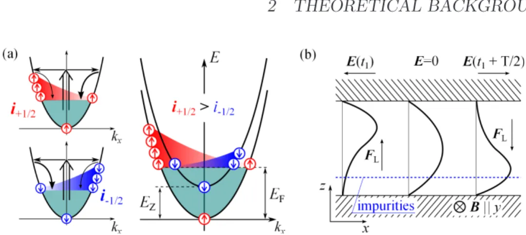
All of them require asymmetric carrier scattering with respect to±kin order to convert THz radiation into adccurrent. The asymmetric scattering, described by the scattering matrix element Wkf,ki, can be caused for instance by spin- related phenomena [43] or by the direct influence of the in-plane magnetic field onto the electron orbitals which is often discussed in terms of a diamagnetic shift [44]. In the following, these two mechanisms are introduced.
Spin-related phenomena: In systems with strong spin-orbit coupling, the scattering matrix elementWkk′ looks as follows [45]
Wkf,ki =W0+X
αβ
wαβσα(ki+kf), (15)
whereW0describes conventional symmetric carrier scattering, the second-rank pseudo tensor wαβ represents the asymmetric spin-dependent scattering and
2.3 Second order photoelectric effects 17 σα is a Pauli-matrix component. The model of the dc current generation is depicted in Fig. 7 (a) for a spin degenerated parabolic dispersion and Drude absorption. The linear coupling between spin (σ) and momentum (kf,ki) leads to spin dependent scattering within spin-up and spin-down subbands and re- sults in asymmetric population of each subband with respect to±k. This spin accumulation can be seen as two fluxes of spin polarized electronsi±1/2 of op- posite directions. However, the total electric current is zero. This mechanism is known as the zero bias spin separation [45].
In order to convert the spin fluxes into a spin-polarized electric current, the spin degeneracy need to be lifted, for instance by an in-plane magnetic field.
The spin up and spin down subbands get energetically separated by the Zee- man energy EZ = gµbB and thus, are unequally occupied. As a result, the spin fluxesi±1/2 due to the asymmetric scattering do not cancel each other any more, leading to a directeddcelectric current which is the result of the MPGE and linear in B.
Diamagnetic contributions: In systems which are characterized by spatial inversion asymmetry (SIA), such as e.g. (001)-oriented QWs grown from zinc- blende-type compounds, Wkf,ki is given by [44]
Wkf,ki =W0+X
αβ
wαβBα(ki+kf), (16)
where Bα is the applied in-plane magnetic field which couples linearly to the carrier momentum. A model system of the dc current generation due to a diamagnetic shift is depicted in Fig. 7 (b). The spatial asymmetry is given by a doping layer which is placed apart from the center of the QW reducing the symmetry of the system in z-direction. In this particular geometry the magnetic field is applied along the y-direction. If an alternating electric field supplied by THz radiation acts on the carriers, they start to move back and forth. The motion in the magnetic field results in a Lorentz force FL which shifts right (left) moving electrons down (up). The up-shifted electrons scat- ter with lower probability than those which are down-shifted towards the δ layer. Thus, within a period of time of the electric field the carriers exhibit a directed motion leading to adc current. Since the orbital shift is provided by
the Lorentz forceFL = (e/c)[v×B], the current is typically linear in B.
The specific mechanism which is responsible for the MPGE is determined by the system under study. In Ref. [46] spin related contributions to the MPGE were studied showing that spin-polarized currents can be strongly enhanced in QW systems with a high electron g-factor (InAs) or dilute magnetic semicon- ductors (DMS) where the exchange interaction between electrons and para- magnetic ions causes an additional contribution to the Zeeman energy known as the giant Zeeman splitting. By contrast, in Ref. [47] it was shown that also the diamagnetic shift can yield a significant contribution to the MPGE in samples which are characterized by a strong structure inversion asymmetry.
The magnetic field induced photogalvanic effects have proven to be a powerful tool to study semiconductor heterostructures, but so far, these effects were not observed in graphene.
19
3 Experimental methods
This chapter is devoted to the experimental methods required for studies of photoelectric phenomena in graphene. At first, the generation of THz radiation by optically pumped molecular THz lasers and free electron lasers (FEL) is pre- sented. Therefore, the underlying effects are explained and the buildup of the devices is shown. Subsequently, the description of the radiation’s polarization state by the Stoke’s parameters and techniques allowing their manipulation are presented. This is followed by the description of the experimental setups where the used optical components, the measurement techniques, and the calibration of the laser systems and - beams are discussed. Finally, the studied samples are presented. Two groups of samples are investigated in the framework of this thesis and hence, their production and preparation methods are explained briefly. Sample parameters which are of importance to explain experimental results are introduced at the end of this chapter.
3.1 Sources of high-power THz radiation
The photoelectric phenomena which are in the focus of this thesis are the result of the light-matter coupling in response to radiation with frequencies ranging from around 100 GHz up to some tens of THz. The corresponding photon energies are roughly situated between 1 and 100 meV. Nowadays, a vast amount of sources of coherent radiation for this range of the electromagnetic spectrum is available. Two sources of high-power THz radiation were chosen for the experiments: i) the optically pumped molecular THz laser [48] providing discrete laser lines in the THz range and output powers of tens of kW and ii) the free electron laser [49], which offers an almost continuously tunable output spectrum from the near- to the far- infrared region. Both sources of THz radiation have proven as powerful tools to study photoelectric phenomena [19].
In the following, the used radiation sources and the basic principles leading to coherent emission of THz radiation are briefly introduced.
3.1.1 Optically pumped molecular THz lasers
The emission of IR/THz laser radiation from molecular transitions was realized in the mid of the 1960s with the development of HCN and H2O lasers [50, 51].
The first optically pumped molecular THz laser was realized in 1969 for contin- uous wave (cw) operation [48] and in 1974 extended to pulsed operation [52].
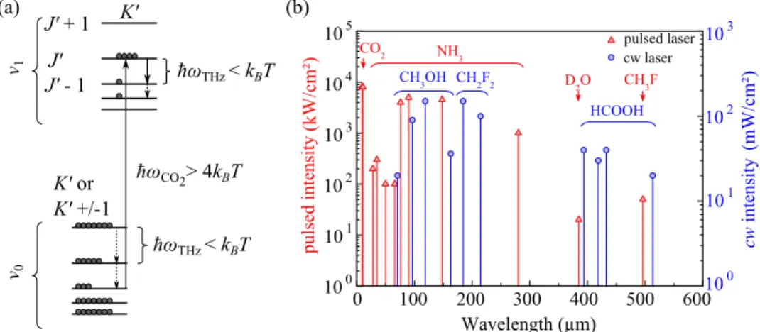
The scheme of the optical transitions leading to population inversion in a molecule is sketched in Fig. 8 (a). Two vibrational levelsν0 and ν1 of different energies are split up into various rotational levels (Erot << Evib) with angu- lar momentum J and K being it’s projection onto the symmetry axis of the molecule. The typical energy separation of the rotational levels in molecules is smaller thankBT ≈ 25 meV and hence, corresponds to THz photon energies.
By optical pumping with a CO2 laser providing laser lines between approx- imately 9.2 and 11.2 µm (Eph ≈ 4kBT) [53] rotational levels in the higher energetic vibrational state ν1 are excited leading to population inversion in both vibrational bands. This population inversion relaxes by emitting photons with energies within the THz range (see arrows in Fig. 8 (a)).
J' J' + 1
J' - 1 K'
v0
K' or K' +/-1
ħωCO2> 4kBT ħωTHz < kBT
ħωTHz < kBT (a)
v1 pulsed intensity cwintensity
(b)
Figure 8: (a) Optical transitions in a molecule between vibrational states ν1 and ν2 which are split up into rotational levels: resonant pumping leads to population inversion between rotational states in both vibrational levels and to emission of THz radiation. (b) available laser lines for pulsed (red) and cw (blue) operations together with corre- sponding output intensities.
3.1 Sources of high-power THz radiation 21 With that principle, plenty of resonant transitions can be achieved by the choice of the molecule and the variation of the pump frequency. Moreover, in the case of high pump power (Ppump ≈ MW) additional laser lines may appear due to the level broadening in the presence of a high electric field [54, 55]. In addition, assisted by stimulated Raman scattering molecular levels can be excited which are distant from the excitation energy depending on the excitation frequency and the gas pressure of the active media [19]. A summary of all laser lines available for the experiments is presented in Fig. 8 (b). It indicates that the optically pumped molecular THz lasers cover the spectral range between 0.6 and 30 THz with several discrete laser lines.
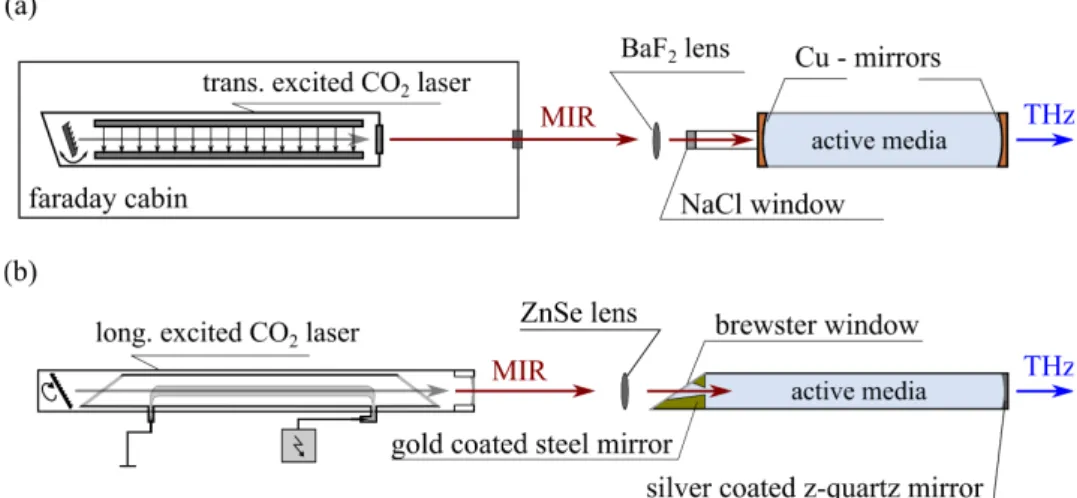
Figure 9: Schemes of (a) pulsed and (b) cw optically pumped mole- cular THz lasers.
Depending on the pump source, either cw or pulsed laser radiation can be generated. Schemes of both types of molecular lasers are depicted in Fig. 9.
To generate pulsed THz radiation a pulsed transversely excited (TEA) CO2 laser [56, 57] serves as a pump source providing pulses with approximately 100 ns duration and powers in the order of tens of MW. With a BaF2 lens the pulses are coupled through a NaCl window into a resonator containing the active media which is built up of a glass tube and two spherical Cu mirrors at each end. The resulting THz pulses are coupled via a TPX window into the free space. The THz pulses have the same temporal shape as the excitation pulses and the typical output power is in the order of tens of kW.
To achieve cw operation, MIR radiation from a longitudinally excited CO2
laser [58] is coupled through a ZnSe Brewster window into the THz resonator by a ZnSe lens. Here, a gold-coated steel mirror and a semi-transparent silver coated z-quartz mirror form the resonator of the laser. The output power which can be achieved with the cw laser is typically in the order of tens of mW. Both types of molecular THz lasers have proven as a powerful tool to study the nonlinear photoelectric phenomena in graphene [28, 30] and were used for the majority of the experiments presented in this thesis.
3.1.2 The free electron laser FELIX
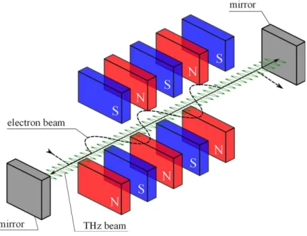
Another source of coherent THz radiation is the free electron laser [59–61].
The emission of radiation results from relativistic electrons which oscillate in a magnetic field.
Figure 10: Scheme of a FEL: an electron beam oscillates in a per- pendicular magnetic field of a Wiggler magnet array (dashed line) and emits THz radiation.
The scheme of a FEL is depicted in Fig. 10. A beam of relativistic electrons (v ≈c) is coupled into an alternating magnetic field of the so called Wiggler
3.1 Sources of high-power THz radiation 23 magnet array. The electrons follow an oscillating trajectory with a periodicity given by the Wiggler period λw due to the action of the magnets. This elec- tron oscillations lead to the emission of radiation. The determination of the radiation’s wavelengthλ can be found e. g. in Ref. [62] and follows to:
λ = λw
2γ2(1 +Kw2/2), (17)
including the relativistic correction γ = 1−(v/c)2−1/2
and the Wiggler strength Kw = eBwλw/2πm0c2. Consequently, the laser wavelength can be tuned by the Wiggler periodicity λw, the magnetic field strength, or the ki- netic energy of the electron beam. The radiation pattern is almost perfectly directed in the direction of motion of the electron beam [63]. A microbunch- ing process resulting from the interaction of the relativistic electrons with the electromagnetic wave leads to the emission of coherent radiation [53].
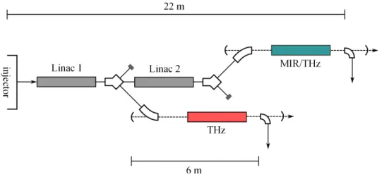
Figure 11: Outline and dimensions of the free electron laser FELIX.
For the experiments, the free electron laser facility FELIX [64] situated at the FOM Institute Rijnhuizen in The Netherlands, was chosen. FELIX was built in 1999 and consists of two FEL lasers covering the total frequency range from 4.5 up to 250 µm. A scheme of the laser facility is shown in Fig. 11. The laser consists of an electron injector and two radio frequency linear accelera- tors (linacs). The first linac provides electron beams with energies up to 25 MeV, the second one delivers beams up to 50 MeV. Wiggler magnet arrays are connected after both the first and the second accelerator yielding radiation
ranging from 5 to 30 µm and from 25 to 250 µm, respectively. The output power can be tuned from 0.5 up to 100 MW within a picosecond micropulse and the overall degree of linear polarization is > 99% for the FEL radiation.
The tunability in a wide frequency range and the high output power makes the free electron laser attractive for experiments on nonlinear photoelectric phenomena in graphene.
3.2 Variation of the light’s polarization state
As discussed in the previous chapter, the photoelectric phenomena under study show complex dependencies on the radiation’s polarization state. Both linearly and circularly polarized radiations may result in a directed electric current. As mentioned above, THz laser radiation is almost perfectly linearly polarized.
Therefore, it is inevitable to manipulate the polarization state of the THz ra- diation. In this section, at the beginning, the description of the polarization state by the Stokes parameters [65] is presented. Only this formalism yields a full description because it includes unpolarized radiation states as well. Af- terwards, experimental methods to vary the radiation’s polarization state are discussed.
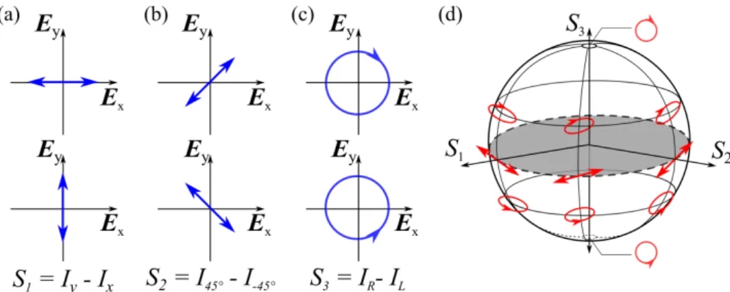
3.2.1 The Stokes parameters
The Stokes parameters are a set of four values which fully describe the polariza- tion state of electromagnetic radiation. A method to introduce the parameters is shown in Fig. 12 (a-c) considering four linear polarizers aligned along x, y, +45◦ and -45◦ and two filters being sensitive to the intensity of either left- or right handed circularly polarized radiation, respectively.
The transmitted intensity I of a laser beam through the six filters defines the Stokes parameters as follows:
S0 =Ix+Iy, (18)
S1 =Ix−Iy, (19)
S2 =I+45−I−45, (20)
S3 =Iright−Ilef t. (21)
3.2 Variation of the light’s polarization state 25
Figure 12: Set of vectors describing the second (a), third (b) and fourth (c) Stokes parameter. (d) Poincar´e sphere describing all possible polarization states on its surface.
The first Stokes parameter, S0, describes the light’s total intensity I. The second,S1, and third parameter,S2, define the state of linear polarization. In detail,S1 indicates whether the polarization is primarily oriented along the x- ory-direction. S2 reveals the components which are aligned in between. The fourth parameter,S3, yields whether the polarization state has any elliptically or even circularly polarized components and vanishes if the radiation is purely linearly polarized. Instead of intensity, also the corresponding electric field components can be used for the description [65]:
S0 =ExEx∗+EyEy∗, (22)
S1 =ExEx∗−EyEy∗, (23)
S2 =ExEy∗+EyEx∗, (24)
S3 =i(ExEy∗−EyEx∗). (25)
Below will be shown that this presentation allows one to recalculate the Stokes parameters into experimentally available parameters such as rotational angles of quarter- and half-wave plates. By choosing S1−3 as the axes of a three- dimensional coordinate system, each polarization state can be described by a point on the surface of the 3D sphere (see Fig. 12 (d)). Linearly polarized radiation states are situated in the S1-S2 plane of the surface. Circularly po- larized states are located at the poles (±|S3|) of the sphere and in between the elliptically polarized radiation states can be found. This sphere is known as
the Poincar´e sphere [66]. In order to describe the full polarization state the parameters are normalized:
p=
pS12 +S22+S32
S0 . (26)
Thus, ifpequals unity the wave is fully polarized whereas in the case it vanishes the radiation is completely unpolarized. In between the wave is partially po- larized. Hence, the Stokes parameters deliver a full description of all possible polarization states. In the following methods to vary the Stokes parameters are presented.
3.2.2 Variation of the Stokes parameters by waveplates
A method to vary the radiation’s polarization state is to use birefringent ma- terials. In the THz range, x-cut crystal quartz can be applied for instance.
θ Ef
Ei
Ei
E E
c-axis
0° 22.5° 45° 67.5° 90°
θ
0° 45° 90° 135° 180°
α Ef Orientation of the linear polarization:
(a) (b)
Figure 13: (a) Geometry of rotation of the linear polarization plane by a λ/2 plate and (b) the final polarization states with respect to the rotational angle θ of the plate. The final azimuth angle of the linearly polarized radiation is α= 2θ.
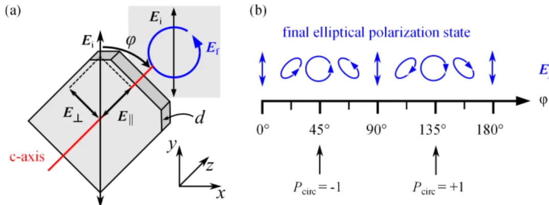
The scheme of the variation of a linearly polarized beam is depicted in Fig. 13.
An incident electric field vectorEi, which is rotated with respect to the crystal- lographic axiscof a quartz plate under a certain angle Θ, can be divided into
3.2 Variation of the light’s polarization state 27 an ordinary beamE⊥, which is aligned perpendicularly toc, and an extraordi- nary beamE||, which is aligned parallel to the axis. For THz frequencies, the refractive index n of quartz is different for E⊥ and E|| and thus, both parts of the beam propagate with different velocities. The resulting phase shift ∆φ between the beam components after passing a plate with a certain thicknessd can be calculated as [67]:
∆φ= (2πd)/λ·∆n, (27)
with ∆n=neo−no being the difference of refractive indices for the extraordi- nary (eo) and ordinary (o) beam, respectively. If ∆φequalsπ/2, the plate acts as quarter-wave /λ/4-plate and produces circularly polarized radiation. In the case ∆φ = π, the plate acts as a half-wave / λ/2-plate and rotates the pola- rization plane of linearly polarized radiation. Experimentally, the polarization state is varied by the rotation of quarter- or half-wave plates. In the case of a half-wave plate, this results in the rotation of an incident electric field vector Ei by an angleαwhich is twice the rotational angleθ of the plate (see Fig. 13).
In the case of a quarter-wave plate,Ei is converted into an elliptically, or even circularly polarized state depending on the rotational angle ϕ (see Fig. 14).
c-axis
E E
Ei Ef
Ei
Pcirc = -1 Pcirc = +1
0° 45° 90° 135° 180°
Ef
final elliptical polarization state
Figure 14: (a) Geometry of conversion of originally linearly into ellip- tically polarized radiation by a λ/4 plate and (b) the final polarization states with respect to the rotational angle ϕof the plate.