Dielectric Engineering of Electronic Correlations in a van der Waals Heterostructure
Philipp Steinleitner,
†Philipp Merkl,
†Alexander Graf,
†Philipp Nagler,
†Kenji Watanabe,
‡Takashi Taniguchi,
‡Jonas Zipfel,
†Christian Schu ̈ ller,
†Tobias Korn,
†Alexey Chernikov,
†Samuel Brem,
§Malte Selig,
∥Gunnar Bergha ̈ user,
§Ermin Malic,*
,§and Rupert Huber*
,††
Department of Physics, University of Regensburg, Universita ̈ tsstraße 31, 93053 Regensburg, Germany
‡
National Institute for Material Science, 305-0044 1-1 Namiki Tsukuba, Ibaraki, Japan
§
Department of Physics, Chalmers University of Technology, Fysikgården 1, 41258 Gothenburg, Sweden
∥
Department of Theoretical Physics, Technical University of Berlin, Hardenbergstraße 36, 10623 Berlin, Germany
*
SSupporting Information
ABSTRACT: Heterostructures of van der Waals bonded layered materials o ff er unique means to tailor dielectric screening with atomic-layer precision, opening a fertile fi eld of fundamental research. The optical analyses used so far have relied on interband spectroscopy. Here we demonstrate how a capping layer of hexagonal boron nitride (hBN) renormalizes the internal structure of excitons in a WSe
2monolayer using intraband transitions. Ultrabroadband terahertz probes sensi- tively map out the full complex-valued mid-infrared con- ductivity of the heterostructure after optical injection of 1s A excitons. This approach allows us to trace the energies and line widths of the atom-like 1s − 2p transition of optically bright and dark excitons as well as the densities of these quasiparticles.
The excitonic resonance red shifts and narrows in the WSe
2/hBN heterostructure compared to the bare monolayer. Furthermore, the ultrafast temporal evolution of the mid-infrared response function evidences the formation of optically dark excitons from an initial bright population. Our results provide key insight into the e ff ect of nonlocal screening on electron − hole correlations and open new possibilities of dielectric engineering of van der Waals heterostructures.
KEYWORDS: Dichalcogenides, atomically thin 2D crystals, van der Waals heterostructures, dielectric engineering, dark excitons.
A tomically thin layers of transition metal dichalcogenides (TMDCs) have been in the spotlight of physical and chemical research due to a unique combination of properties. In particular, TMDC monolayers exhibit a direct energy gap in the optical range
1,2in sharp contrast to gapless graphene, which makes them fascinating candidates for ultimately thin optoelectronic devices.
3−5Interestingly, the electronic and optical properties of this material system are dominated by Coulomb-bound electron − hole pairs, called excitons,
6,7rather than by unbound charge carriers. Reduced Coulomb screening in combination with the reduced dimensionality of atomically thin crystals leads to a dramatic increase of the exciton binding energy to typical values of few hundred millielectronvolts, stabilizing these states even at room temperature.
7−13Owing to the extreme con fi nement perpendicular to the plane of the material, excitons are particularly sensitive to the local environment surrounding the monolayer.
14−22The possibility to vertically stack di ff erent cover materials onto two-dimen- sional TMDCs
4,23has thus opened an exciting platform for fundamental physics
20,24−32and device technologies.
33,34On the one hand, heterostructures consisting of two di ff erent
semiconducting monolayers have been employed to realize ultrathin p − n junctions
33and interlayer excitons
24,26,35due to the possibility of interlayer charge transfer.
24,26,33,35On the other hand, TMDC monolayers covered with an insulating van der Waals material have allowed for a less invasive strategy of Coulomb engineering.
17,20By dielectric sculpting of the electric fi eld lines connecting electrons and holes, in-plane electronic correlations can be modi fi ed within the TMDC monolayer without changing the chemical structure of the material itself.
20Electron−phonon interactions
30,31,36,37may be controlled and in-plane heterostructures can be realized on a nanometer length scale.
17,20The most widespread methods of investigating excitons probe their interband generation or annihilation.
7,10,11In these experiments, light couples dominantly to only a minor fraction of excitons, namely the optically bright ones. Optically dark states, whose interband dipole moment vanishes or whose
Received: December 6, 2017 Revised: January 19, 2018 Published: January 24, 2018
pubs.acs.org/NanoLett Cite This:Nano Lett.XXXX, XXX, XXX−XXX
© XXXX American Chemical Society A DOI:10.1021/acs.nanolett.7b05132
Nano Lett.XXXX, XXX, XXX−XXX
center-of-mass momenta lie outside the light cone, cannot be directly addressed this way and have required more sophisticated in-plane propagation geometries
38or phonon- assisted processes.
37Mid-infrared (mid-IR) photons, in contrast, may directly induce a hydrogen-like 1s − 2p transition in pre-existing species, irrespective of interband dipole moments and large center-of-mass momenta. This concept has been employed to explore the formation time and dynamics of excitons in TMDC monolayers
12,13,39,40and also represents a promising tool for the investigation of electronic correlations in heterostructures. Still, the direct in fl uence of a cover layer on the correlations between orbital states of excitons has not been resolved in a direct, resonant way.
In this Letter, we experimentally investigate the in fl uence of an insulating hexagonal boron nitride cover layer on the fundamental intraexcitonic 1s − 2p resonance by the absorption of mid-IR photons in the TMDC monolayer WSe
2. By utilizing intraband spectroscopy, we are able to address all excitons in the system, including bright and dark states. This approach allows us to reveal the in fl uence of the cover layer and its dielectric constant on the internal structure of excitons in the most direct possible way. We fi nd that an hBN cover layer leads to a signi fi cant renormalization of the intraexcitonic 1s − 2p transition by 23 meV and a decrease of the transition line width compared to the uncovered monolayer. Moreover, the ultrafast evolution of the mid-IR response functions shows a distinct blue shift of the intraexcitonic 1s − 2p resonance transition and an increase of its line width with time. Using microscopic modeling, we show that these observations are characteristic of
the formation of dark excitons from the initial bright population.
The WSe
2/hBN heterostructure (Figure 1a) is manufactured by mechanical exfoliation and van der Waals bonding.
41First, a monolayer of WSe
2is deterministically transferred from a viscoelastic substrate onto a CVD diamond window. Sub- sequently, the cover layer is added onto the monolayer in the same way. The homogeneous distribution of the photo- luminescence (PL) intensity across the WSe
2fl ake (Figure 1b) con fi rms the structural integrity of the monolayer after being covered with hexagonal boron nitride. Furthermore, the corresponding PL intensity spectrum (Figure 1c, black solid curve) features a peak energy of 1656 meV and a line width of 47 meV (fwhm). A comparison of these values to a PL spectrum of an uncovered monolayer (Figure 1c, black dashed curve) shows that covering reduces the line width of the PL by 5%, but hardly a ff ects its spectral position. These observations are in line with recent interband spectroscopy results.
18−20,22,35The thickness of the hBN cover layer is 100 nm, measured with atomic force microscopy.
To explore the in fl uence of the capping layer on the electronic correlations in the WSe
2monolayer, especially the fundamental intraexcitonic transition, we resonantly create bright 1s A excitons
12by optical excitation with a 100 fs laser pulse centered at a wavelength of 745 nm (1664 meV, Supporting Information Figure S1). The pump fl uence is set to Φ = 27 μ J/cm
2in order to keep the excitation density at a moderate level.
40For the direct observation of the hydrogen- like 1s − 2p transition of the injected excitons, we use phase- Figure 1. (a) Artist’s view of the sample structure. A WSe
2monolayer (blue and black spheres) on a CVD diamond window is covered with a capping layer of hexagonal boron nitride (hBN, thickness: 100 nm). The WSe
2/hBN heterostructure is fabricated by mechanical exfoliation of the individual components and subsequent deterministic transfer from a viscoelastic substrate onto a CVD diamond substrate. (b) Optical microscopy image and room-temperature PL intensity map of the WSe
2/hBN heterostructure excited by a continuous-wave laser at a wavelength of 532 nm. The lateral dimensions of the WSe
2monolayer are about 100 μm × 75 μm. (c) Corresponding PL intensity spectrum (black solid curve) compared to the PL spectrum of a bare monolayer (black dashed curve). (d) Waveform of the phase-stable single-cycle mid-IR probe pulse E
reftransmitted through the unexcited heterostructure as a function of the electro-optic gate delay time t
EOS. (e) Corresponding multioctave spanning amplitude (black curve) and phase spectrum (red curve) as obtained by Fourier transformation of E
ref(t
EOS).
DOI:10.1021/acs.nanolett.7b05132 Nano Lett.XXXX, XXX, XXX−XXX B
locked single-cycle mid-IR pulses (Figure 1d) generated by optical recti fi cation of the fundamental laser output in a 10- μ m- thin GaSe crystal. The pulses feature a flat spectral phase (Figure 1e, red curve) throughout their multioctave spanning amplitude spectrum ranging from photon energies between 30 and 165 meV (Figure 1e, black curve). By electro-optic sampling up to the mid-IR spectral region, the absolute amplitude and phase of the transmitted electric fi eld waveform E
ref(t
EOS) are recorded as a function of the detection time t
EOS. We compare the mid-IR probe transient through the excited and the unexcited sample and determine the pump-induced change Δ E(t
EOS) for a given delay time t
PPbetween pumping and probing. The amplitude of Δ E is typically on the order of a few times 10
−3compared to the peak of E
ref. A continuous
variation of t
PPprovides access to the ultrafast dynamics of the nonequilibrium system (Supporting Information Figure S2). All experiments are performed at room temperature and ambient conditions.
From the quantities E
ref(t
EOS) and Δ E(t
EOS, t
PP) the complex- valued mid-IR response function of the resonantly excited heterostructure can be extracted via a transfer matrix formal- ism.
42,43The mid-IR response function includes the change in the real parts of the mid-IR conductivity ( Δσ
1) and the dielectric function ( Δε
1), roughly corresponding to absorptive and inductive components, respectively. The advantage of the fi eld-sensitive detection is that both functions can be extracted independently, without resorting to a Kramers − Kronig analysis.
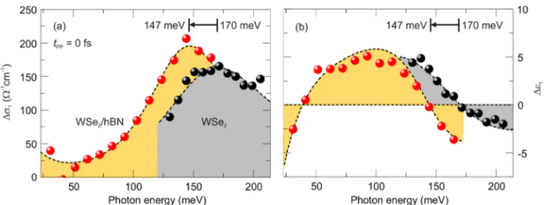
Figure 2. Pump-induced changes of the real parts of the optical conductivity Δσ
1(a) and the dielectric function Δε
1(b) as a function of the photon energy, for a fi xed pump delay time t
PP= 0 fs after resonant excitation. The red spheres (yellow shading) denote the experimental data of the photoexcited WSe
2/hBN heterostructure (pump fl uence Φ = 27 μ J/cm
2), whereas the black spheres (gray shading) describe the experimental data of a photoexcited monolayer (pump fl uence Φ = 25 μ J/cm
2, taken from ref 12). The black dashed curves represent the results by a phenomenological Drude − Lorentz model (eq 1) fi tting simultaneously Δσ
1and Δε
1. This model takes unbound electron − hole pairs as well as excitons into account.
13The arrows indicate the shift of the resonance from 170 meV (bare monolayer) to 147 meV (hBN covered monolayer).
Figure 3. Pump-induced changes of the real parts of the optical conductivity Δσ
1(a−d) and the dielectric function Δε
1(e−h) as a function of the photon energy, for several pump delay times t
PPafter resonant excitation. The red spheres (yellow shading) denote the experimental data of the photoexcited WSe
2/hBN heterostructure (pump fluence Φ = 27 μJ/cm
2). The black dashed curves represent the results of a phenomenological Drude−Lorentz model (eq 1) fitting simultaneously Δσ
1and Δε
1.
DOI:10.1021/acs.nanolett.7b05132 Nano Lett.XXXX, XXX, XXX−XXX C
We will show below that these features originate from the renormalized 1s − 2p transition of the resonantly generated excitons.
The nature of the screened excitons also manifests itself in their dynamics. Figure 3 displays the ultrafast evolution of the mid-IR response of the WSe
2/hBN heterostructure for a series of delay times t
PP. Compared to the response at t
PP= 0 fs (Figure 3a,e), the overall magnitude of the signal decreases, the resonance blue shifts slightly and the line width broadens as a function of t
PP(Figure 3b − d,f − h). Interestingly, a second zero crossing in Δε
1persists on the low-frequency end of the spectral window for all pump delay times t
PP. This feature may be caused by a second low-energy resonant absorption or by unbound electron − hole pairs, whose contribution would have a similar e ff ect on Δε
1.
For a more quantitative evaluation of the measured mid-IR response functions (Figures 2 and 3), we apply a Drude − Lorentz model
13,44,45re fl ecting the contribution of excitons (Lorentz) and an electron − hole plasma (Drude) on a phenomenological level. Within this approach, pump-induced changes in the frequency-dependent dielectric function Δε ( ω )
= Δε
1+ i Δσ
1/( ε
0ω ) are described using two components
ε ω ε μ ω ω ε μ ω ω
Δ =
− − Δ
− + Γ
ℏ
n e d
f i
n e
d i
( ) 1
E X
2
0
1s,2p 2
FC 2
0 2
res 2 2
(1) The fi rst term, a Lorentzian resonance, represents the intraexcitonic 1s − 2p line. It includes the 1s exciton density n
X, the corresponding reduced mass μ = m
em
h/(m
e+m
h) (m
eand m
hare the e ff ective masses of the constituent electron and hole), the e ff ective thickness d of the monolayer (treated as a thin slab in this model), the oscillator strength f
1s,2pof the intraexcitonic transition, the resonance energy E
res, and the line width Δ . Additional constants are the electron charge e and the vacuum permittivity ε
0. The second term represents the Drude response of the electron − hole plasma, which depends on the density of free carriers n
FCand their scattering rate Γ . For the analysis of the data, we fi x the reduced mass μ = 0.17 m
0and the oscillator strength for the covered monolayer f
1s,2phetero= 0.30 ( f
1s,2pbare= 0.32 see ref 12), corresponding to electron − hole properties at the K and K ′ valleys in WSe
2. The e ff ective monolayer thickness d is set to 0.7 nm. The remaining parameters of the Drude − Lorentz model (n
X, n
FC, E
res, Δ , Γ ) are extracted by fi tting the experimental data. The fact that both independently measured Δσ
1and Δε
1spectra need to be simultaneously reproduced poses strict limits on the possible values of the fi tting parameters. The numerical adaptation (Figures 2 and 3, black dashed curves) yields an overall good fi t quality. Note that this model has been well established for a
For the bare monolayer, the fi tting procedure of the experimental data at a pump delay time t
PP= 0 fs (Figure 2a,b, black spheres) yields an exciton density of 3.63 × 10
12cm
−2, a resonance energy of 170 meV, and a line width of 117 meV. There is no measurable contribution from unbound electron − hole pairs in the investigated spectral region, in agreement with previous works.
12,13In contrast, adding the hBN cover layer red shifts the resonance E
resto 147 meV, whereas the line width Δ decreases to 90 meV at t
PP= 0 fs (Figure 2a,b, red spheres). Furthermore, the fi t of the heterostructure data reveals a nonvanishing density of unbound electron − hole pairs n
FC.
Figure 4 summarizes the complete temporal evolution of the fi tting parameters n
X, n
FC, Δ and E
resfor the WSe
2/hBN heterostructure. The density of excitons (Figure 4a, black spheres) initially decays within the fi rst hundreds of femto- seconds from n
X= 3.93 × 10
12cm
−2to 2.15 × 10
12cm
−2followed by a much slower decay on a picosecond scale.
12This dynamics corresponds to the radiative recombination of coherent bright excitons followed by the decay of incoherent dark states.
12,47The pump-induced change Δ E observed at a fi xed electro-optic sampling time t
EOS= 0 fs (Figure 4a, black solid line) has been established to be proportional to the exciton density.
12,13Thus, recording Δ E(t
EOS= 0 fs) as a function of t
PPprovides an alternative access to the temporal evolution of the exciton density. The almost perfect agreement of the temporal shape of n
X(t
PP) (Figure 4a, black spheres) with Δ E(t
EOS= 0 fs, t
PP) (Figure 4a, black solid line) further corroborates the phenomenological Drude − Lorentz model of eq 1.
The density of unbound electron − hole pairs n
FC(Figure 4a, red spheres) rises within the first 200 fs, starting from a nonvanishing value n
FC= 0.1 × 10
12cm
−2, and slowly decays on a much longer time scale. Furthermore, n
FCis an order of magnitude smaller than n
Xfor all pump delay times t
PP. As noted above, the e ff ect of a fi nite plasma density may also indicate the presence of a Lorentzian line located below the spectral window accessed here and will be further investigated in future research. The temporal evolution of the resonance energy E
resis depicted in Figure 4b. Starting from an initial value of 147 meV at t
PP= 0 fs, E
resblue shifts up to 153 meV at t
PP= 2 ps. The line width Δ , however, decreases from 90 to 80 meV, within 200 fs, followed by a monotonic increase up to Δ = 112 meV at t
PP= 2 ps (Figure 4c).
Both the spectral response and its ultrafast evolution provide novel evidence of renormalized Coulomb correlations shaped by the dielectric screening, as we show next. To explain the pronounced red shift of the intraexcitonic 1s − 2p transition energy of the heterostructure by 23 meV, we perform calculations on a microscopic level explicitly taking into account the dielectric constant of the surrounding diamond
DOI:10.1021/acs.nanolett.7b05132 Nano Lett.XXXX, XXX, XXX−XXX D
substrate and the hBN cover layer. In the case of the heterostructure, we expect increased screening of the Coulomb potential compared to the bare monolayer, which should result in a reduction of the binding energy of excitons and thus in a red shift of the 1s − 2p transition energy. Solving the excitonic Wannier equation in momentum representation
36μ ∑
ℏ Ψ
α− Ψ
α+ =
α αΨ
q q V q k q k E q
2 ( ) ( , ) ( ) ( )
k 2 2
exc
(2) we have microscopic access to exciton binding energies E
αand wave functions Ψ
α( q ) with index α = 1s, 2s, 2p, ... . Here, we have introduced the excitonic part of the Coulomb interaction V
exc( q , k ), which is treated within the thin- fi lm formalism for 2D systems.
8,9,14,48,49The latter also contains the dielectric background screening ε
BG=
ε +ε2
cover substrate
of the underlying substrate/cover layer.
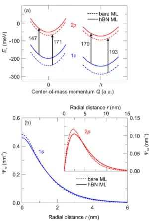
Figure 5a shows the calculated binding energies of 1s and 2p states of intravalley K − K excitons (parabolae around Q = 0) as well as momentum-forbidden dark K- Λ excitons (parabolae around Q = Λ ) as a function of the center-of-mass momentum Q. Broken (solid) curves indicate the situation for the bare (hBN covered) monolayer. The corresponding radial wave functions for bright excitons (Q = 0) are depicted in Figure 5b.
We can perfectly reproduce the experimentally observed 1s − 2p
resonance energy of 147 meV at t
PP= 0 fs for bright K − K excitons with a dielectric constant of ε
cover= 2.3, which agrees well with the literature value for hBN.
50Thus, we can unequivocally assign the observed resonance at 147 meV to the renormalized 1s − 2p transition in the heterostructure.
The ultrafast evolution of the resonance energy E
resshows a monotonic blue shift with increasing pump delay time t
PP(Figure 4b). This feature can be explained by the formation of a momentum-forbidden dark intervalley exciton population via exciton − phonon scattering or the emergence of spin-unlike excitons due to spin- fl ip processes.
40Since the intraexcitonic 1s − 2p separation of dark K −Λ excitons is higher than the one of the initially bright excitons (Figure 5a), E
resincreases as the dark population forms.
40Furthermore, the dark excitonic ground state (Q = Λ ) in WSe
2is energetically lower than the bright one (Q = 0, Figure 5a) leading to an e ffi cient accumulation of K −Λ excitons during thermalization.
40Next we turn to the strong reduction of the line width Δ from 117 meV for the bare monolayer to 90 meV for the heterostructure at t
PP= 0 fs. This fact appears even more striking when the corresponding exciton densities are considered. Δ is expected to increase with n
X.
12,13In our experiment, the line width Δ
heterois found to be smaller than Δ
bareby 23%, even though the density n
Xheteroslightly exceeds n
Xbareby 8%. Thus, the hBN cover layer clearly reduces the width of the intraexcitonic 1s − 2p transition line. One of the possible broadening mechanisms contributing to the line width Figure 4. (a) Temporal evolution of the exciton density n
X(black
spheres, excitons) and the unbound electron−hole pair density n
FC(red spheres, free carriers) as extracted from fitting the mid-IR response function of the WSe
2/hBN heterostructure (Figure 3, red spheres) measured for different pump delay times t
PPwith the Drude- Lorentz model. The pump-induced change ΔE recorded at fixed electro-optic sampling time t
EOS= 0 fs (ΔE
max, black solid line) is proportional to the exciton density n
X. Resonance energy E
res(b) and line width Δ (c) as a function of the pump delay time t
PPas obtained from fitting the experimental mid-IR response data of the heterostructure (Figure 3, red spheres). The error bars represent the 95% confidence intervals of the fitting parameters.
Figure 5. (a) Calculated binding energies E
α(α = 1s, 2p) for intravalley K−K excitons (parabolae around Q = 0) as well as momentum-forbidden dark K−Λ excitons (parabolae around Q = Λ) as a function of the center-of-mass momentum Q. The black arrows symbolize various intraexcitonic 1s−2p transitions. (b) Calculated radial wave functions Ψ
α(r) for the 1s (blue curves) and 2p (red curves) bright excitonic levels (Q = 0). The dashed lines are related to the bare monolayer, whereas the solid lines refer to calculations for the monolayer covered with hBN.
DOI:10.1021/acs.nanolett.7b05132 Nano Lett.XXXX, XXX, XXX−XXX E
decrease of the line width Δ . Exciton − exciton scattering, however, depends on the Coulomb potential which is indirectly proportional to ε
BG. Thus, the increase of ε
BG, caused by adding a cover layer, can lead to a decrease of exciton − exciton scattering, resulting in a smaller line width Δ.
The temporal evolution of the line width (Figure 4c) shows another unexpected behavior. Δ should decrease as a function of t
PPbecause the overall electron − hole pair density decreases (Figure 4a as well as Supporting Information Figures S3 and S4) and thus fewer scattering events take place. However, the line width after an initial and expected decrease starts to rise from 80 meV at t
PP= 0.2 ps to 112 meV at t
PP= 2 ps. This anomalous behavior is a second indication for dark intervalley or spin-unlike excitons both having higher resonance energies than the bright states.
40Because our mid-IR probe pulse is sensitive to all kinds of dark excitons, the superposition of various intraexcitonic 1s − 2p absorption peaks from di ff erent momentum- or spin-forbidden states leads to an apparent increase of the line width, as the dark population (t
PP> 0.2 ps) forms from the initial bright exciton population (t
PP< 0.2 ps).
Since the overall electron − hole pair density steadily decreases for t
PP> 0.2 ps (Figure 4a) and thus the line width Δ should show a similar trend, the observed strong blue shift of E
rescan only be accounted for by the formation of dark excitons.
40In conclusion, intraband spectroscopy in the mid-IR spectral range allows us to investigate the in fl uence of the modi fi cation of the dielectric environment on bright and dark excitons in a WSe
2monolayer. The data quantify internal transition energies, densities and many-body e ff ects. Most remarkably, we observe a signi fi cant red shift of the intraexcitonic 1s − 2p transition as well as a decrease of its line width compared to the uncovered monolayer. Furthermore, the distinct blue shift of the 1s − 2p resonance along with the anomalous dynamics of the line width suggests the formation of a dark exciton population from an initial bright one. These heterostructures fabricated by simple stacking o ff er an exciting playground to custom-tailor electronic correlations and thus open exciting perspectives for novel optoelectronic applications. In future studies yet sharper resonances may be achieved by full encapsulation of the monolayer with hBN.
19Furthermore, one may even resonantly hybridize excitonic transitions with low-energy excitation of surrounding cover layers, designing novel material parameters by layer-sensitive dielectric sculpting.
■ ASSOCIATED CONTENT
*
SSupporting Information
The Supporting Information is available free of charge on the ACS Publications website at DOI: 10.1021/acs.nano- lett.7b05132.
Kenji Watanabe: 0000-0003-3701-8119
Samuel Brem: 0000-0001-8823-1302
Malte Selig: 0000-0003-0022-412X Notes
The authors declare no competing fi nancial interest.
■ ACKNOWLEDGMENTS
The authors thank Matthias Knorr for helpful discussions and Martin Furthmeier for technical assistance. The work in Regensburg was supported by the European Research Council through Grant 305003 (QUANTUMsubCYCLE) as well as by the Deutsche Forschungsgemeinschaft (through Grants HU1598/2-1, KO3612/1-1, SFB 1277, projects A05, B05, and B06, and GRK 1570). A.C. gratefully acknowledges funding from the Deutsche Forschungsgemeinschaft through the Emmy Noether Programme (CH1672/1-1). The Chalmers group acknowledges funding from the European Union ’ s Horizon 2020 research and innovation program under Grant Agreement 696656 (Graphene Flagship) and the Swedish Research Council (VR). The Berlin group was supported by the Deutsche Forschungsgemeinschaft (DFG) through the collaborative research centers SFB 787 and 951. K.W. and T.T.
acknowledge support from the Elemental Strategy Initiative conducted by the MEXT, Japan and JSPS KAKENHI Grant JP15K21722.
■ (1) Splendiani, A.; Sun, L.; Zhang, Y.; Li, T.; Kim, J.; Chim, C.-Y.; REFERENCES Galli, G.; Wang, F. Emerging Photoluminescence in Monolayer MoS2. Nano Lett. 2010, 10, 1271 − 1275.
(2) Mak, K. F.; Lee, C.; Hone, J.; Shan, J.; Heinz, T. F. Atomically Thin MoS
2: A New Direct-Gap Semiconductor. Phys. Rev. Lett. 2010, 105, 136805.
(3) Wang, Q. H.; Kalantar-Zadeh, K.; Kis, A.; Coleman, J. N.; Strano, M. S. Electronics and optoelectronics of two-dimensional transition metal dichalcogenides. Nat. Nanotechnol. 2012, 7, 699 − 712.
(4) Britnell, L.; Ribeiro, R. M.; Eckmann, A.; Jalil, R.; Belle, B. D.;
Mishchenko, A.; Kim, Y.-J.; Gorbachev, R. V.; Georgiou, T.; Morozov, S. V.; et al. Strong Light-Matter Interactions in Heterostructures of Atomically Thin Films. Science 2013, 340, 1311 − 1314.
(5) Ross, J. S.; Klement, P.; Jones, A. M.; Ghimire, N. J.; Yan, J.;
Mandrus, D. G.; Taniguchi, T.; Watanabe, K.; Kitamura, K.; Yao, W.;
Cobden, D. H.; Xu, X. Electrically tunable excitonic light-emitting diodes based on monolayer WSe
2p − n junctions. Nat. Nanotechnol.
2014, 9, 268 − 272.
(6) Ramasubramaniam, A. Large excitonic effects in monolayers of molybdenum and tungsten dichalcogenides. Phys. Rev. B: Condens.
Matter Mater. Phys. 2012, 86, 115409.
(7) He, K.; Kumar, N.; Zhao, L.; Wang, Z.; Mak, K. F.; Zhao, H.;
Shan, J. Tightly Bound Excitons in Monolayer WSe
2. Phys. Rev. Lett.
2014, 113, 026803.
(8) Berkelbach, T. C.; Hybertsen, M. S.; Reichman, D. R. Theory of neutral and charged excitons in monolayer transition metal
DOI:10.1021/acs.nanolett.7b05132 Nano Lett.XXXX, XXX, XXX−XXX F
dichalcogenides. Phys. Rev. B: Condens. Matter Mater. Phys. 2013, 88, 045318.
(9) Berghäuser, G.; Malic, E. Analytical approach to excitonic properties of MoS
2. Phys. Rev. B: Condens. Matter Mater. Phys. 2014, 89, 125309.
(10) Ye, Z.; Cao, T.; O’Brien, K.; Zhu, H.; Yin, X.; Wang, Y.; Louie, S. G.; Zhang, X. Probing excitonic dark states in single-layer tungsten disulphide. Nature 2014, 513, 214 − 218.
(11) Chernikov, A.; Berkelbach, T. C.; Hill, H. M.; Rigosi, A.; Li, Y.;
Aslan, O. B.; Reichman, D. R.; Hybertsen, M. S.; Heinz, T. F. Exciton Binding Energy and Nonhydrogenic Rydberg Series in Monolayer WS
2. Phys. Rev. Lett. 2014, 113, 076802.
(12) Poellmann, C.; Steinleitner, P.; Leierseder, U.; Nagler, P.;
Plechinger, G.; Porer, M.; Bratschitsch, R.; Schu ̈ ller, C.; Korn, T.;
Huber, R. Resonant internal quantum transitions and femtosecond radiative decay of excitons in monolayer WSe
2. Nat. Mater. 2015, 14, 889−893.
(13) Steinleitner, P.; Merkl, P.; Nagler, P.; Mornhinweg, J.; Schüller, C.; Korn, T.; Chernikov, A.; Huber, R. Direct Observation of Ultrafast Exciton Formation in a Monolayer of WSe
2. Nano Lett. 2017, 17, 1455−1460.
(14) Cudazzo, P.; Tokatly, I. V.; Rubio, A. Dielectric screening in two-dimensional insulators: Implications for excitonic and impurity states in graphane. Phys. Rev. B: Condens. Matter Mater. Phys. 2011, 84, 085406.
(15) Fang, H.; Battaglia, C.; Carraro, C.; Nemsak, S.; Ozdol, B.;
Kang, J. S.; Bechtel, H. A.; Desai, S. B.; Kronast, F.; Unal, A. A.; et al.
Strong interlayer coupling in van der Waals heterostructures built from single-layer chalcogenides. Proc. Natl. Acad. Sci. U. S. A. 2014, 111, 6198 − 6202.
(16) Ugeda, M. M.; Bradley, A. J.; Shi, S.-F.; Da Jornada, F. H.;
Zhang, Y.; Qiu, D. Y.; Ruan, W.; Mo, S.-K.; Hussain, Z.; Shen, Z.-X.;
et al. Giant bandgap renormalization and excitonic effects in a monolayer transition metal dichalcogenide semiconductor. Nat. Mater.
2014, 13, 1091−1095.
(17) Ro ̈ sner, M.; Steinke, C.; Lorke, M.; Gies, C.; Jahnke, F.;
Wehling, T. O. Two-Dimensional Heterojunctions from Nonlocal Manipulations of the Interactions. Nano Lett. 2016, 16, 2322 − 2327.
(18) Stier, A. V.; Wilson, N. P.; Clark, G.; Xu, X.; Crooker, S. A.
Probing the Influence of Dielectric Environment on Excitons in Monolayer WSe
2: Insight from High Magnetic Fields. Nano Lett. 2016, 16, 7054−7060.
(19) Cadiz, F.; Courtade, E.; Robert, C.; Wang, G.; Shen, Y.; Cai, H.;
Taniguchi, T.; Watanabe, K.; Carrere, H.; Lagarde, D.; et al. Excitonic Linewidth Approaching the Homogeneous Limit in MoS
2-Based van der Waals Heterostructures. Phys. Rev. X 2017, 7, 021026.
(20) Raja, A.; Chaves, A.; Yu, J.; Arefe, G.; Hill, H. M.; Rigosi, A. F.;
Berkelbach, T. C.; Nagler, P.; Schu ̈ ller, C.; Korn, T.; et al. Coulomb engineering of the bandgap and excitons in two-dimensional materials.
Nat. Commun. 2017, 8, 15251.
(21) Borghardt, S.; Tu, J.-S.; Winkler, F.; Schubert, J.; Zander, W.;
Leosson, K.; Kardynał, B. E. Engineering of optical and electronic band gaps in transition metal dichalcogenide monolayers through external dielectric screening. Phys. Rev. Mater. 2017, 1, 054001.
(22) Ajayi, O. A.; Ardelean, J. V.; Shepard, G. D.; Wang, J.; Antony, A.; Taniguchi, T.; Watanabe, K.; Heinz, T. F.; Strauf, S.; Zhu, X.-Y.;
et al. Approaching the Intrinsic Photoluminescence Linewidth in Transition Metal Dichalcogenide Monolayers. 2D Mater. 2017, 4, 031011.
(23) Geim, A. K.; Grigorieva, I. V. Van der Waals heterostructures.
Nature 2013, 499, 419 − 425.
(24) Rivera, P.; Schaibley, J. R.; Jones, A. M.; Ross, J. S.; Wu, S.;
Aivazian, G.; Klement, P.; Seyler, K.; Clark, G.; Ghimire, N. J.; et al.
Observation of long-lived interlayer excitons in monolayer MoSe
2- WSe
2heterostructures. Nat. Commun. 2015, 6, 6242.
(25) Dufferwiel, S.; Schwarz, S.; Withers, F.; Trichet, A. A. P.; Li, F.;
Sich, M.; Del Pozo-Zamudio, O.; Clark, C.; Nalitov, A.; Solnyshkov, D.
D.; et al. Exciton-polaritons in van der Waals heterostructures embedded in tunable microcavities. Nat. Commun. 2015, 6, 8579.
(26) Chen, H.; Wen, X.; Zhang, J.; Wu, T.; Gong, Y.; Zhang, X.;
Yuan, J.; Yi, C.; Lou, J.; Ajayan, P. M.; et al. Ultrafast formation of interlayer hot excitons in atomically thin MoS
2/WS
2heterostructures.
Nat. Commun. 2016, 7, 12512.
(27) Rivera, P.; Seyler, K. L.; Yu, H.; Schaibley, J. R.; Yan, J.;
Mandrus, D. G.; Yao, W.; Xu, X. Valley-polarized exciton dynamics in a 2D semiconductor heterostructure. Science 2016, 351, 688−691.
(28) Raja, A.; Montoya-Castillo, A.; Zultak, J.; Zhang, X.-X.; Ye, Z.;
Roquelet, C.; Chenet, D. A.; Van der Zande, A. M.; Huang, P.;
Jockusch, S.; et al. Energy Transfer from Quantum Dots to Graphene and MoS
2: The Role of Absorption and Screening in Two- Dimensional Materials. Nano Lett. 2016, 16, 2328−2333.
(29) Hill, H. M.; Rigosi, A. F.; Rim, K. T.; Flynn, G. W.; Heinz, T. F.
Band Alignment in MoS
2/WS
2Transition Metal Dichalcogenide Heterostructures Probed by Scanning Tunneling Microscopy and Spectroscopy. Nano Lett. 2016, 16, 4831−4837.
(30) Jin, C.; Kim, J.; Suh, J.; Shi, Z.; Chen, B.; Fan, X.; Kam, M.;
Watanabe, K.; Taniguchi, T.; Tongay, S.; et al. Interlayer electron- phonon coupling inWSe
2/hBN heterostructures. Nat. Phys. 2017, 13, 127−131.
(31) Chow, C. M.; Yu, H.; Jones, A. M.; Yan, J.; Mandrus, D. G.;
Taniguchi, T.; Watanabe, K.; Yao, W.; Xu, X. Unusual Exciton-Phonon Interactions at van der Waals Engineered Interfaces. Nano Lett. 2017, 17, 1194−1199.
(32) Manca, M.; Glazov, M. M.; Robert, C.; Cadiz, F.; Taniguchi, T.;
Watanabe, K.; Courtade, E.; Amand, T.; Renucci, P.; Marie, X.; et al.
Enabling valley selective exciton scattering in monolayer WSe
2through upconversion. Nat. Commun. 2017, 8, 14927.
(33) Lee, C.-H.; Lee, G.-H.; Van der Zande, A. M.; Chen, W.; Li, Y.;
Han, M.; Cui, X.; Arefe, G.; Nuckolls, C.; Heinz, T. F.; et al.
Atomically thin p − n junctions with van der Waals heterointerfaces.
Nat. Nanotechnol. 2014, 9, 676−681.
(34) Withers, F.; Del Pozo-Zamudio, O.; Mishchenko, A.; Rooney, A.
P.; Gholinia, A.; Watanabe, K.; Taniguchi, T.; Haigh, S. J.; Geim, A. K.;
Tartakovskii, A. I.; et al. Light-emitting diodes by band-structure engineering in van der Waals heterostructures. Nat. Mater. 2015, 14, 301−306.
(35) Rigosi, A. F.; Hill, H. M.; Li, Y.; Chernikov, A.; Heinz, T. F.
Probing Interlayer Interactions in Transition Metal Dichalcogenide Heterostructures by Optical Spectroscopy: MoS
2/WS
2and MoSe
2/ WSe
2. Nano Lett. 2015, 15, 5033−5038.
(36) Selig, M.; Bergha ̈ user, G.; Raja, A.; Nagler, P.; Schu ̈ ller, C.;
Heinz, T. F.; Korn, T.; Chernikov, A.; Malic, E.; Knorr, A. Excitonic linewidth and coherence lifetime in monolayer transition metal dichalcogenides. Nat. Commun. 2016, 7, 13279.
(37) Christiansen, D.; Selig, M.; Bergha ̈ user, G.; Schmidt, R.;
Niehues, I.; Schneider, R.; Arora, A.; De Vasconcellos, S. M.;
Bratschitsch, R.; Malic, E.; Knorr, A. Phonon Sidebands in Monolayer Transition Metal Dichalcogenides. Phys. Rev. Lett. 2017, 119, 187402.
(38) Wang, G.; Robert, C.; Glazov, M. M.; Cadiz, F.; Courtade, E.;
Amand, T.; Lagarde, D.; Taniguchi, T.; Watanabe, K.; Urbaszek, B.;
et al. In-Plane Propagation of Light in Transition Metal Dichalcogenide Monolayers: Optical Selection Rules. Phys. Rev. Lett.
2017, 119, 047401.
(39) Cha, S.; Sung, J. H.; Sim, S.; Park, J.; Heo, H.; Jo, M.-H.; Choi, H. 1s-intraexcitonic dynamics in monolayer MoS
2probed by ultrafast mid-infrared spectroscopy. Nat. Commun. 2016, 7, 10768.
(40) Berghäuser, G.; Steinleitner, P.; Merkl, P.; Huber, R.; Knorr, A.;
Malic, E. Mapping of the dark exciton landscape in transition metal dichalcogenides. 2017, arxiv 1708.07725, accessed 1/9/2018.
(41) Castellanos-Gomez, A.; Buscema, M.; Molenaar, R.; Singh, V.;
Janssen, L.; Van der Zant, H. S. J.; Steele, G. A. Deterministic transfer of two-dimensional materials by all-dry viscoelastic stamping. 2D Mater. 2014, 1, 011002.
(42) Huber, R.; Tauser, F.; Brodschelm, A.; Bichler, M.; Abstreiter, G.; Leitenstorfer, A. How many-particle interactions develop after ultrafast excitation of an electron-hole plasma. Nature 2001, 414, 286−
289.
DOI:10.1021/acs.nanolett.7b05132 Nano Lett.XXXX, XXX, XXX−XXX G
−
(47) Selig, M.; Bergha ̈ user, G.; Richter, M.; Bratschitsch, R.; Knorr, A.; Malic, E. Dark and bright exciton formation, thermalization, and photoluminescence in monolayer transition metal dichalcogenides.
2017, arxiv 1703.03317, accessed 1/9/2018.
(48) Rytova, N. S. Screened potential of a point charge in a thin film.
Mosc. Univ. Phys. Bull. 1967, 3, 30.
(49) Keldysh, L. V. Coulomb interaction in thin semiconductor and semimetal films. JETP Lett. 1979, 29, 658 − 661.
(50) Kim, K. K.; Hsu, A.; Jia, X.; Kim, S. M.; Shi, Y.; Dresselhaus, M.;
Palacios, T.; Kong, J. Synthesis and Characterization of Hexagonal Boron Nitride Film as a Dielectric Layer for Graphene Devices. ACS Nano 2012, 6, 8583 − 8590.
DOI:10.1021/acs.nanolett.7b05132 Nano Lett.XXXX, XXX, XXX−XXX H