Studies of
Read-Out Electronics and Trigger for Muon Drift Tube Detectors
at High Luminosities
von
Sebastian Nowak
eingereicht an der
Fakult¨at f¨ur Physik
der
Technischen Universit¨at M¨unchen
erstellt am
Max-Planck-Institut f¨ur Physik (Werner-Heisenberg-Institut)
M¨unchen
Juni 2015
Max-Planck-Institut f¨ur Physik (Werner-Heisenberg-Institut)
Studies of Read-Out Electronics and Trigger for Muon Drift Tube Detectors at High Luminosities
Sebastian Nowak
Vollst¨ andiger Abdruck der von der Fakult¨at f¨ ur Physik der Technischen Universit¨ at M¨ unchen zur Erlangung des akademischen Grades eines
Doktors der Naturwissenschaften (Dr. rer. nat.) genehmigten Dissertation.
Vorsitzender: Univ.-Prof. Dr. A. Ibarra Pr¨ ufer der Dissertation:
1. Priv.-Doz. Dr. H. Kroha 2. Univ.-Prof. Dr. L. Oberauer
Die Dissertation wurde am 22.06.2015 bei der Technischen Universit¨ at M¨ unchen eingereicht
und durch die Fakult¨at f¨ ur Physik am 25.06.2015 angenommen.
The Large Hadron Collider (LHC) at the European Centre for Particle Physics, CERN, collides protons with an unprecedentedly high centre-of-mass energy and luminosity. The collision products are recorded and analysed by four big experiments, one of which is the ATLAS detector. For precise measurements of the properties of the Higgs-Boson and searches for new phenomena beyond the Standard Model, the LHC luminosity of L = 10
34cm
−2s
−1is planned to be increased by a factor of ten leading to the High Lumi- nosity LHC (HL-LHC). In order to cope with the higher background and data rates, the LHC experiments need to be upgraded.
In this thesis, studies for the upgrade of the ATLAS Muon Spectrometer are presented with respect to the read-out electronics of the Monitored Drift Tube (MDT) and the small-diameter Muon Drift Tube (sMDT) chambers and the Level-1 muon trigger. Due to the reduced tube diameter of sMDT chambers, background occupancy and space charge effects are suppressed by an order of magnitude compared to the MDT chambers.
The rate capability of the sMDT chambers is limited by signal pile-up effects of the MDT read-out electronics using bipolar signal shaping. In order to profit from the full potential of sMDT chambers, prototype read-out electronics with improved signal shaping and baseline restoration has been developed. Measurement and simulation of the sMDT drift-tubes with the new read-out electronics show that the high-rate performance of the sMDT chambers is substantially increased.
At HL-LHC, muon trigger rates are expected to be about 10 times higher than at the
LHC design luminosity. In order to fully exploit the physics potential of the HL-LHC,
the selectivity of the ATLAS Muon Trigger system has to be improved. This is achieved
by using the MDT chambers of the ATLAS Muon Spectrometer in the muon trigger to
obtain the optimum achievable muon momentum resolution in the trigger. Simulations
and measurements with a demonstrator of the MDT based trigger at the CERN Gamma
Irradiation Facility demonstrate the feasibility of this concept.
Abstract 5
1. Motivation and Outline 9
2. The Large Hadron Collider 11
3. The ATLAS Muon Spectrometer 13
3.1. The Muon Detectors . . . 13
3.2. The Trigger and Data Acquisition System . . . 14
3.2.1. The Level-1 Trigger . . . 14
3.2.2. The High-Level Trigger . . . 15
3.3. Background Radiation in the Muon Spectrometer . . . 16
3.4. Upgrade of the ATLAS Detector at High Luminosity . . . 17
3.4.1. Upgrade of the Trigger and Data Acquisition System . . . 18
4. Muon Drift-Tube Chambers 19 4.1. Monitored Drift Tube Chambers . . . 19
4.1.1. MDT Chamber Read-out Electronics . . . 21
4.2. Small-Diameter Muon Drift Tube Chambers . . . 23
4.2.1. Spatial Resolution and Muon Efficiency . . . 24
4.3. High-Rate Phenomena . . . 25
4.3.1. Space Charge Effects . . . 25
4.3.2. Read-Out Electronics Effects . . . 26
5. Optimisation of Drift-Tube Read-Out Electronics for High Counting Rates 31 5.1. Signal Shaping . . . 31
5.1.1. Unipolar and Bipolar Signal Shaping . . . 31
5.1.2. Baseline Restoration . . . 32
5.2. The ASD Chip . . . 33
5.3. A Discrete Pulse Shaper for sMDT Tubes (ASBC) . . . 36
5.3.1. The ASBC Circuit . . . 37
5.3.2. Comparison of ASD and ASBC δ-Response . . . 43
5.3.3. ASBC Response for a Parametrised Pulse . . . 44
5.3.4. Response Simulation . . . 46
5.3.5. Threshold Determination . . . 49
5.3.6. Noise Considerations . . . 50
5.4. Performance of the ASBC Electronics at High Counting Rates . . . 54
5.4.1. Experimental Setup . . . 56
5.4.2. Data Analysis . . . 57
5.4.3. Simulation of the Performance of the sMDT Read-Out Electronics . 66 5.4.4. Results . . . 68
5.4.5. Performance under Irradiation with
137Cs . . . 72
5.4.6. Conclusion and Outlook . . . 74
6. Drift-Tube Based First-Level Muon Trigger for ATLAS at HL-LHC 77 6.1. The ATLAS Muon Trigger at the LHC . . . 77
6.2. The Concept of an MDT Based Level-1 Muon Trigger . . . 80
6.3. Algorithm for the Fast Muon Track Reconstruction . . . 81
6.3.1. Initial Considerations . . . 81
6.3.2. Fast Track Reconstruction Algorithm . . . 82
6.3.3. Monte-Carlo Simulation Studies . . . 86
6.3.4. Performance of the Fast Read-out with Experimental Data . . . 92
6.3.5. Timing Performance Estimation . . . 101
6.4. Further Considerations . . . 114
6.4.1. Bunch Crossing Identification . . . 114
6.4.2. Hough transform based pattern recognition . . . 117
6.5. Conclusion and Outlook . . . 121
Summary 123 A. Appendix 125 A.1. Parametrisation of the Space-Drift-Time Relationship . . . 125
A.2. Read-Out Electronics for Drift-Tubes . . . 126
A.2.1. Unipolar and Bipolar Shaping Scheme . . . 126
A.2.2. The RC-Circuit . . . 127
A.2.3. Operational Amplifier Based Differentiator . . . 128
A.2.4. The ASBC . . . 131
A.2.5. Stage 1 . . . 135
A.2.6. Stage 2 . . . 135
A.2.7. Diode Model Determination (SPICE) . . . 136
A.2.8. Simulation . . . 136
A.3. Performance of the Trigger Demonstrator Set-up . . . 139
A.4. ARM Cortex-M4F Implementation of the Track Finding Algorithm . . . 141
Bibliography 149
Acknowledgements 155
The Organization shall provide for collaboration among European States in nuclear research of a pure scientific and fundamental character, and in research essentially related thereto. The Organization shall have no concern with work for military requirements and the results of its experimental and theoretical work shall be published or otherwise made generally available.
(CERN Convention, Article 2 [1]) Since the foundation of CERN
1in 1953 many important discoveries in particle physics have been made. In 1983 the W- and Z-Bosons were discovered by the UA1 and UA2 ex- periments using proton-antiproton collisions in the Super-Proton Synchrotron (SPS) which started operation in 1976. Between 1989 and 2000 Large Electron-Positron Collider (LEP) was operated at CERN with four experiments which performed precision measurements of the electroweak interaction.
With the start of the Large Hadron Collider (LHC) a new era for particle physics has begun. The first highlight was the discovery of the Higgs-Boson in 2012 [2, 3]. For precise measurements of the Higgs-Boson properties and searches for new phenomena beyond the Standard Model the centre-of-mass energy of the LHC will be raised to 13 TeV in 2015 and the luminosity will be increased in several steps over the next ten years (see Section 2).
The luminosity increase necessities upgrades of LHC experiments.
In this thesis, studies for the upgrade of the ATLAS Muon Spectrometer are presented, in particular of the Level-1 muon trigger and of the read-out electronics of the Monitored Drift Tubes (MDT) chambers and small-diameter Muon Drift Tube (sMDT) chambers.
After a short introduction about the LHC, the ATLAS Experiment and the planned luminosity upgrades, the principles of the MDT and sMDT chambers are discussed in Chapter 4. In Chapter 5, improvements of their read-out electronics for operation at high luminosities are presented. Chapter 6 is devised to studies of using the MDT chambers in the ATLAS Level-1 muon trigger.
1
Conseil Europ´een pour la Recherche Nuclaire
The Large Hadron Collider (LHC) [4], colliding protons in a circular storage ring of 27 km circumference since end of 2009, is the largest scientific instrument ever build. The accel- erated protons of the LHC circle the ring in bunches with a design separation in time of 25 ns corresponding to a bunch crossing rate of 40 MHz. In addition to the proton beams, the LHC can also accelerate and collide heavy ion beams, in particular lead ions. The LHC is designed for a nominal instantaneous luminosity of L
0= 10
34cm
−2s
−1of proton-proton collisions at a centre-of-mass energy of 14 TeV with 2808 bunches of protons [5].
The LHC has been built in the already existing accelerator tunnel of the Large Electron Positron Collider (LEP) which has been shut down at the end of 2000. The already ex- isting pre-accelerators are being reused, namely the LINAC2, the BOOSTER, the Proton Synchrotron (PS) and the Super Proton Synchrotron (SPS). An overview of the CERN accelerator complex is given in Fig. 2.1.
The LHC started at a center-of-mass energy of 900 GeV end of 2009 and 7 TeV in 2010. In 2012, the center-of-mass energy was raised to 8 TeV. A peak luminosity of about L = 8 · 10
33cm
−1s
−1was also reached in 2012.
Without an additional LHC luminosity increase the running time necessary to half the statistical error in the measurements will be more than a decade. Therefore, the LHC luminosity has to be increased [7], the planned time-line (2014) is shown in Fig. 2.2. It is planned to upgrade the LHC in several steps. In Run 2 the LHC is going to be operated slightly below its design energy. During the one year LS 2 the Phase-1 upgrade is going to take place, leading afterwards to a luminosity increase of a factor of 3. Finally, between 2023 and 2025 the Phase-2 upgrade is going to lead to the so-called High-Luminosity LHC (HL-LHC). The main objective of the HL-LHC is to reach a peak luminosity of L = 5 · 10
34cm
−2s
−1with levelling, leading to a integrated luminosity of 250f b
−1per year and to 3000f b
−1over 12 years [7].
Due to the luminosity increase after the upgrades, the LHC experiments have to be adapted to cope with the changed conditions. Therefore, LS1 and LS2 are also used to upgrade the experiments and conduct the necessary maintenance.
The implications of the Phase-2 upgrade for the ATLAS Muon Spectrometer and the
development of new detector components to operate under the changed conditions are
discussed in the following.
!
" #
$"" %
#
%
&
!
'( ) '( ) * + , + -
. ' / ** / '! 0 + '! +
' '# + * * +1' ' + * 0 % ' ' ' ' ' '" * '# - +
' *
2 '% . ' ' 3 ' 4' * .
Figure 2.1.: Overview of the CERN accelerator complex [6]. Starting with LINAC2 and the BOOSTER and after pre-acceleration in the PS and SPS, the protons are injected into the LHC ring.
Figure 2.2.: Planned time schedule of the LHC high luminosity upgrades [8]. Upgrades to
Phase-1 and Phase-2 (HL-LHC) take place during the Long shutdowns LS2
amd LS3, respectively. The green boxes represent the accumulated integrated
luminosity of the accelerator.
The goals of the ATLAS
1experiment [9] (see Fig. 3.1) are to measure Standard Model processes indicating Higgs boson production and decays with high precision and to discover new physics beyond. With a length of 44 m, a diameter of 25 m and a weight of 7000 tons, the ATLAS detector is the largest experiment at the LHC. Its construction took place between May 2003 and end of 2008.
3.1. The Muon Detectors
The Muon Spectrometer [10] is the outer-most and largest part of the ATLAS detector (see Fig. 3.1 and Fig. 3.3). It provides precise muon track and momentum reconstruction with a momentum resolution of
∆p
Tp
T< 10
−4p
GeV (3.1)
for p
T> 300 GeV and
∆p
Tp
T< 3% (3.2)
for p
T< 300 GeV [10]. The resolution in the lower momentum range is limited by multiple scattering in the detector structures and by energy loss fluctuations in the calorimeters.
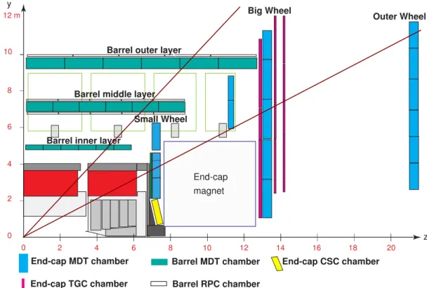
The Muon Spectrometer is split into the barrel and two end-cap regions (see Fig. 3.3), each with three layers of precision tracking detectors. The barrel consists of inner, middle and outer layers, each end-cap of a Small Wheel, Big Wheel and the Outer Wheel. With the exception of the very forward regions of the Small Wheels where cathode strip chambers (CSC) are used, the muon tracking detectors are Monitored Drift Tube (MDT) chambers (see Section 4).
To achieve the required muon momentum resolution in the toroidal magnetic field of the Muon Spectrometer, the track points in each layer have to be measured with an accuracy of better than 50 µm. This sets the requirements on the intrinsic resolution and the mechanical precision of the MDT chambers [10] (see Section 4.1). In addition, the operating parameters, the relative alignment of the chambers and the magnetic field strength have to be monitored with high precision to be taken into account in muon track reconstruction.
1
ATLAS - A Toroidal LHC AparatuS
Figure 3.1.: Cut-away view of the ATLAS detector [9]. The inner tracking detector and the calorimeters for particle and jet energy measurements are surrounded by the Muon Spectrometer consisting of three layers of muon chambers in a toroidal magnetic field of superconducting air-core magnets.
Special, fast trigger chambers are used for the Level-1 muon trigger, Resistive Plate Chambers (RPC) in the middle and outer layers of the barrel and Thin Gap Chambers (TGC) in the end-caps. They also measure the track coordinates along the MDT drift- tubes with reduced resolution.
3.2. The Trigger and Data Acquisition System
The ATLAS trigger system consists of three levels. A simplified overview of the trigger and DAQ system is given in Fig. 3.4.
3.2.1. The Level-1 Trigger
The Level-1 (L1) trigger decision is based on reduced-granularity information from the calorimeter and muon trigger chambers (see Section 3.1). As shown in Fig. 3.4, the decisions of calorimeter and muon trigger are combined in the Central Trigger Processor.
In addition, the L1 trigger provides Regions of Interest (RoI) which are passed on to the
next trigger level. During the L1 trigger latency of 2.5 µs, the information of all detector
Figure 3.2.: Cut-away view of the ATLAS Muon Spectrometer. RPCs and TGCs are used as trigger chambers, CSCs and MDTs are used for precision measurement [9].
read-out channels is kept in buffers of the front-end electronics (FE). The front-end system was originally designed for a maximal Level-1 trigger rate of 75 kHz. It has been upgraded to a maximal rate of 100 kHz in 2014 [11].
Finally, the event data selected by the Level-1 trigger is read-out from the FE buffers into the read-out buffers (ROBs) via the readout drivers (RODs). The Level-1 trigger decision is based on combinations of calorimeter and muon detector informations [12]. The trigger implementation is programmable to adjust to varying luminosities and background conditions.
3.2.2. The High-Level Trigger
The High-Level Trigger consists of two parts: The Level-2 trigger and the Event Filter (EF).
The Level-2 trigger uses the RoI information provided by the Level-1 trigger which in-
cludes the position (η, φ), the transverse momentum (p
T) range and the energy sums of
Figure 3.3.: Schematic view of one quadrant of the ATLAS muon spectrometer. The red lines indicate tracks of muons with infinite momentum. They typically traverse three detector layers allowing for a track sagitta measurement.
calorimeter cells belonging to candidate objects. While the RoI information is transmitted for all events selected by the Level-1 trigger over a dedicated data path, the data required in order to make the Level-2 trigger decision is accessed selectively. The Level-2 trigger has access to the complete event data with the full granularity, but typically needs only data from a small fraction of the detector.
The ROBs keep the complete data of the selected bunch crossing until the event is rejected or accepted by the Level-2 Trigger. The Event Filter (EF) applies the full offline reconstruction algorithms to the complete event data. Events selected by the EF are sent to mass storage while rejected trigger events are deleted.
3.3. Background Radiation in the Muon Spectrometer
The ATLAS muon detectors are exposed to unprecedentedly high background radiation of
photons and of neutrons with typical energies of 1 MeV which originate from interactions
of the collision products in the detector and the shielding of the beams and is uncorrelated
in time with the bunch-crossings and fills the whole detector cavern [13].
Figure 3.4.: Schematic overview of the trigger and DAQ system for collision data taking operations [12] (see text).
In the Muon Spectrometer the highest background rates occur in the innermost detector layers of the end-cap regions. The impact of the background radiation on the operation of the Monitored Drift Tube chambers is discussed in Section 4.3. This uncorrelated background radiation increases proportionally with the luminosity.
3.4. Upgrade of the ATLAS Detector at High Luminosity
Due to the the increased luminosity at the HL-LHC (see Section 2), the ATLAS detector has to be upgraded to cope with the increasing event rates and background radiation. The main limitations of the currently installed detectors are the lifetimes of the components, the increasing background, the increasing event and background rates and the radiation damage to detectors and electronic components.
Besides the inner tracking detector, which will be completely replaced for Phase-II be- cause of radiation damage and increasing particle rates, the calorimeter and muon detector electronics as well as the trigger and data acquisition supplies have to be upgraded [14].
Developments for the MDT chamber read-out electronic and the new MDT-based Level-1
muon trigger are discussed in this thesis.
Figure 3.5.: Block diagram of the split Level-0/Level-1 trigger proposed for ATLAS Phase- II operation [14]. The MDT trigger may also be implemented already at Level-0.
3.4.1. Upgrade of the Trigger and Data Acquisition System
In order to cope with HL-LHC luminosities, it is planned to upgrade the ATLAS trigger system for Phase-II operation with splitting of the current Level-1 trigger into Level-0 and Level-1 [14].
The following properties are envisaged [14]:
• The Level-0 trigger provides the functionality of the current Level-1 trigger with an output rate of 500 kHz after a latency of 6 µs.
• The Level-1 trigger reduces the event rate to at least 200 kHz within an additional latency of at least 20 µs
2. The rate reduction is accomplished by new track trigger in the inner detector within a RoI provided by the Level-0 trigger.
• The High-Level trigger uses offline-reconstruction algorithms to reduce the final read- out rate to 5-10 kHz.
A block diagram of the architecture of the ATLAS Level-0 and Level-1 trigger system for the Phase-2 operation is shown in Fig. 3.5. The Level-1 Calorimeter trigger will have access to the full calorimeter granularity. The Level-1 Muon trigger will use the MDT precision tracking chambers to sharpen the trigger threshold as a function of p
Tof the muons. The Level-1 Central Trigger Processor finally combines the results of the individual Level-1 trigger systems.
2
A latency of 60 µs is in discussion (begin 2014).
The majority of the precision tracking chambers in the ATLAS Muon Spectrometer are Monitored Drift Tube (MDT) chambers [10]. These kind of particle tracking detectors, which are high accuracy wire chambers and, therefore, commonly used in high-energy particle physics [15], provide high tracking efficiency and spatial resolution, but their performance suffers at high counting rates. Hence, drift-tube chambers with reduced tube diameter for the operation at high background rates have been developed. The first two of this small-diameter Muon Drift tube (sMDT) chambers have been installed in the ATLAS detector in 2014 [16]. More sMDT chambers are currently under construction for installation in 2017 and 2018/19 [17, 18]. Functionality and performance of MDT and sMDT chambers are discussed in the following.
4.1. Monitored Drift Tube Chambers
MDT chambers consists of aluminium drift-tubes assembled into two multi-layers with 3 or 4 layers each (see Fig. 4.1b). The tungsten-rhenium anode wire in the centre is set to a potential of 3080 V with respective to the tube wall. The main MDT parameters are listed in Tab. 4.1.
When a muon passes through an MDT tube, the Argon atoms are ionised along the path of the particle. A 100 GeV muon creates on average about 100 clusters separated typically by 100 µm per cm of typically 3 electrons in it [19]. The ionisation electrons drift towards the wire in the electric field, the ions to the tube wall (see Fig. 4.1a). The electric field strength increases with
1rtowards the wire. In the vicinity of the wire, the field is strong enough for the drifting ionisation electrons to gain enough energy to ionise the Ar gas atoms, leading to an avalanche of secondary electrons and amplification of the primary ionisation charge. For a potential of 3080 V between tube wall and anode wire of the MDT tubes, the gas gain is 20000. The passing muon can also knock out an electron from an atom of the tube wall, a so called δ-electron, which frequently passes the tube at a shorter distance to the wire than the muon (see Fig. 4.2a) masking the muon hit and leading to wrong drift-time measurement.
The minimal distance between muon track and wire can be determined by measuring the
time between the muon passing and the ionised signal arriving at the wire (see Fig. 4.1a)
and using a calibrated space-to-drift-time relation. In Fig. 4.6 the drift-time spectrum
recorded with a uniformly irradiated MDT tube is shown. The drift velocity of the elec-
trons depends on the drift gas. Therefore, the purity of the gas is important for the precise
drift distance measurement.
(a) (b)
Figure 4.1.: (a) Cross section of an MDT tube and (b schematic view of an ATLAS MDT chamber in the barrel region) [9].
Parameter MDT design value sMDT design value
Tube material Aluminium
Outer tube diameter 29.970 mm 15.0 mm
Tube wall thickness 0.4 mm
Wire material gold-plated W/Re (97/3)
Wire diameter 50 µm
Gas mixture Ar/CO
2/H
2O (93/7/ ≤ 1000 ppm)
Gas pressure 3 bar (absolute)
Gas gain 20000
Wire potential +3080 V +2730 V
Maximum drift-time ∼ 700 ns ∼ 185 ns
Average drift-tube resolution 80 µm 105 µm
Table 4.1.: Parameters of the MDT and sMDT chambers [9].
(a) (b)
Figure 4.2.: (a) Illustration of the effect of δ-electrons [20]. A muon knocks an electron out of the tube wall which may cross the tube closer to the wire than the muon and, therefore, masks the real muon hit leading to a wrong drift-time measurement.
(b) Principle of track reconstruction in the drift-tube chambers. The track is fitted to the measured drift-radii [20].
Fig. 4.2b illustrates the muon track reconstruction by minimising the distances between track and measured drift-circles (see also Section 6.3.5.5).
4.1.1. MDT Chamber Read-out Electronics
Fig. 4.3 gives an overview of the electronics circuits connected to the drift-tubes. The electrical connections are implemented on so-called hedgehog boards which supply 24 tubes each. One end of the tube is used for high-voltage supply and is terminated with the drift-tube impedance of 383 Ω to avoid signal reflections. Noise is suppressed with a low-pass filter. At the other end of the tube, the signal is capacitively decoupled from the high-voltage and further processed by active read-out electronics circuits on the so-called Mezzanine boards [21], which each contains three 8-channel ASD
1chips which amplify and shape the signal (see Section 5) and send the digital signal to a Time-to-Digital converter (TDC) if the analogue pulse is above a predefined threshold. In order to minimise noise, the ASD circuits are differential. A block diagram of one channel is shown in Fig. 4.4.
Parameters of the chip can be set using the JTAG
2protocol. Besides the discriminator threshold, the most important parameter is the artificial (programmed) dead time after a pulse exceeding the threshold which can be set between a minimum of 220 ns and a maximum of 820 ns and is discussed in Section 4.3.2.1. For a detailed description of all ASD parameters see [22].
1
Amplifier Shaper Discriminator
2
Joint Test Action Group, IEEE 1149.1 Standard Test Access Port and Boundary-Scan Architecture
Figure 4.3.: Electrical connections to an ATLAS MDT tube [21]. One end of the tube is used for high-voltage supply and terminated with the drift-tube impedance of 383 Ω to avoid signal reflections. The other end of the tube, the signal is capacitively decoupled from the high voltage and processed by preamplifier and shaper circuits on the so-called Mezzanine boards.
The ASD chip provides two options to determine the input charge from the shaped signal.
The first one is to measure the time interval during which the signal is above the threshold and the second one is to measure the pulse charge using a Wilkinson ADC [22] at the first threshold crossing time of the signal.
The digital output pulses of the ASD are sent to a 24-channel Time-to-Digital-Converter (TDC) on the Mezzanine card, which measures the threshold crossing time corresponding to the arrival time of the ionisation signal of the wire with respect to the trigger signal.
The ATLAS Muon Spectrometer uses the AMT-3 chip [23] as TDC.
Up to 18 AMT chips, corresponding to 432 MDT channels (the maximum number of channels of an MDT chamber in ATLAS), are read out by a so-called Chamber Service Module (CSM) on the chamber. The CSM transmits the LHC clock and trigger signals (TTC
3) and JTAG code to the ASD-chips and the temperature sensor measurements on the Mezzanine cards to the detector control system (DCS) via the ELMB
4. The data of the TDCs are sent via an optical fibre from the CSM to a read-out driver (MROD
5) module for further processing [21]. An overview of the whole read-out chain is shown in Fig. 4.5.
For further details on the ATLAS MDT read-out system and its performance see [21, 24].
3
Timing Trigger and Control
4
Embedded Local Monitor Board
5
MDT Readout Driver
Figure 4.4.: Block diagram of one ASD channel [21]. The incoming signal is amplified, bipolar shaped (see Section 5) and digitised. The ASD chip can be operated in (1) time over threshold or (2) charge measurement mode. The ASD can be configured using the JTAG protocoll. The digital output of threshold crossing time is LVDS.
4.2. Small-Diameter Muon Drift Tube Chambers
The MDT chambers installed in the ATLAS Detector show a very good efficiency and resolution up to the highest background counting rates expected at the LHC design lumi- nosity. But at much higher background rates as expected at the high-luminosity upgrade of the LHC (HL-LHC) they suffer from a degradation of the spatial resolution and muon detection efficiency (see Section 4.3). Therefore, drift-tube chambers with reduced tube diameter of 15 mm, so-called small-Diameter Muon Drift Tube (sMDT) chambers have been developed. For compatibility reasons, all other drift-tube parameters, especially gas mixture and pressure and the gas gain, are kept the same (see Tab. 4.1). Due to the smaller diameter, the wire potential has to be decreased to 2730 V in order to obtain the gas amplification of 20000.
The drift-tubes with the two times smaller diameter are expected to two times lower
hit rate at the same background flux. The maximum drift-time of sMDT tubes is only
about 185 ns [27], a factor of ∼ 3.8 smaller than for MDT tubes. Altogether, the drift-tube
occupancy is reduced by a factor of 2 · 3.8 = 7.6. In addition, the reduced tube diameter
leads to strong suppression of space-charge effects [25] deteriorating the spatial resolution
(see Section 4.3) and allows for higher redundancy and efficiency in track segment recon-
struction due to the up to two times larger number of tube layers fitting into the same
volume. The average spatial resolution without background irradiation is slightly worse
by about 20 µm compared to MDT tubes (see Fig. 4.7) due to the shorter average drift
distances (see Fig. 4.9).
Figure 4.5.: Block diagram of the on-chamber data processing with Mezzanine boards, CSM, ELMB, TTC, and MROD [21]. While the TTC trigger signals and the data transmissions are to the MROD, the connections to the CSM are through the passive interconnect.
4.2.1. Spatial Resolution and Muon Efficiency
The performance of the sMDT tubes has already been studied extensively using the stan- dard MDT read-out electronics [28–30].
Fig. 4.7 and Fig. 4.8 show the average MDT and sMDT single-tube spatial resolution and 3σ muon detection efficiency
6depending on the flux and counting rate of photon conversions, respectively. In addition, the sMDT resolution is shown with the requirement
∆t > 600 ns on the time interval between two successive hits, which is equivalent to operation with a dead time of 600 ns.
The read-out electronics behaviour has a strong impact on the resolution and 3σ-efficiency of the sMDT tubes at very high background rates. The sMDT resolution and efficiency depend strongly on the electronics dead time and the signal shaping. By optimisation of signal shaping the resolution and efficiency at high background rates of the sMDT tubes operated with short dead time settings can be improved significantly (see Section 5).
6
The probability for a hit to be measured on the extrpolated muon trajectory within three times the
drift-tube spatial resolution as a function of the drift-radius.
Figure 4.6.: Drift-time spectra of MDT and sMDT tubes operated with Ar:CO2 (93:7) gas mixture at 3 bar absolute pressure and a gas gain of 20000 [25]. The measurement with cosmic ray muons is compared with simulation (Garfield [26]) for the 15 mm diameter tubes.
4.3. High-Rate Phenomena
Most of the hits in the MDT chambers are caused by the γ and neutron background radiation in the ATLAS cavern (see Section 3.3), which cause space charge of slow drifting ions in the tubes and mask muon hits due to the dead time of the read-out electronics.
4.3.1. Space Charge Effects
The ion space charge in the drift-tubes caused by the background hits modifies the electric field and, hence, the drift-velocity and the gas amplification. Due to the stochastic nature of the background hits, the space charge and, therefore, the drift velocity vary in time, leading to a degradation of the spatial resolution increasing with the drift-distance. This effect of space charge fluctuations, which cannot be taken into account in calibration of the space to drift-time relationship, is shown in Fig. 4.9.
The shielding of the wire potential by the ion space charge leads to loss in gas gain (see Fig. 4.10), smaller signals and, therefore, degradation of the time resolution. This effect dominates for muon tracks passing the tube close to the wire.
Close to the tube wall, the effect of space charge and, consequently, of the electric field
and of the drift-velocity on the spatial resolution dominates [32].
Figure 4.7.: Average spatial resolution of 1 m long sMDT and MDT drift-tube depending on the flux of background photon conversions for different electronics dead time settings of the read-out electronics [27]. In addition, the sMDT resolution is shown for the requirement ∆t > 600 ns on the time interval between two successive hits is shown, which is equivalent to operation with a dead time of 600 ns. Solid coloured lines show the simulated sMDT resolution for different dead time settings.
4.3.2. Read-Out Electronics Effects
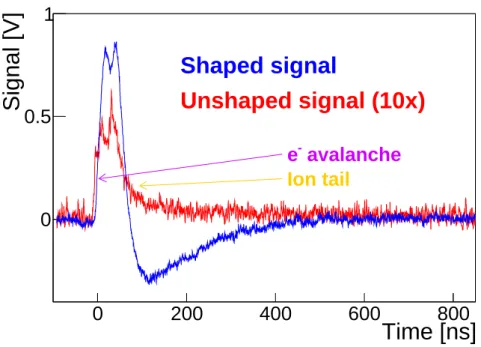
In Fig. 4.11 a typical amplified signal from an sMDT tube muon is shown. The fast rising leading edge is caused by the electron avalanche, while the slowly drifting ions cause the long trailing edge of the unshaped pulse.
Due to the different arrival times of the ionisation electron clusters along the muon
path, the signals can show several peaks which may result in several discriminator thresh-
old crossings while only the first threshold crossing time is of interest for the drift-time
measurement. In order to suppress these secondary discriminator threshold crossings, elec-
tronics dead time programmable between a minimum of 220 ns and a maximum of 820 ns
which covers the maximum drift-time of the MDT tubes during which electron clusters
may arrive, is used in the ASD chip (see Section 5.2).
Figure 4.8.: 3σ-efficiency of MDT and sMDT tubes depending on the dead time-corrected background γ counting rate (see Section 4.3.2.1) for minimum and maximum electronics dead time settings of the ASD chip [27]. The analytic calculation is based on Eq. 4.4.
Without additional signal shaping, the tails cause a shift of the baseline at high counting rates. From different signal shaping options (see Section 5.1), the ASD uses bipolar shaping (see the blue curve in Fig. 4.11). Bipolar shaping differentiates the signal suppressing low frequencies. It provides baseline stability up to high rates, but causes an undershoot with a length corresponding to the length of the ion tail.
4.3.2.1. Dead Time Effects
During the electronics dead time τ , the read-out electronics is insensitive to any further hits arriving. Therefore, the muon detection efficiency decreases with increasing background rate depending on the dead time. When m is the true counting rate and k counts are registered in a read-out time window T , a total dead time kτ is accumulated, since each detected hit triggers the electronics dead time. During the total dead time, mkτ counts are lost. The true number of hits in the time window is (see [33])
mT = k + mkτ , (4.1)
Figure 4.9.: Radial dependence of the MDT spatial resolution for different photon irradia- tion rates [31]. The degradation of the resolution with increasing background flux due to fluctuations of the space charge and, therefore, of the drift-field is limited to the region r > 6 mm and increases with the drift distance. Loss of gas gain due to shielding of the wire potential decreases the signal amplitude which leads to a worsening of the resolution in particular near the wire.
leading to
m =
k T
1 −
Tkτ . (4.2)
Taking into account the linear dependence of the muon efficiency on the observed counting rate r =
Tkǫ(r) = ǫ
0· (1 − r · τ ) , (4.3) where ǫ
0is the muon efficiency in the case of negligible hit rate, one obtains
ǫ(m) = ǫ
01 + mτ . (4.4)
The observed and the true counting rate differ because also background hits are masked
by preceding hits. In order to obtain maximum efficiency, the dead time has to be as short
as possible while minimising the probability for secondary threshold crossings.
Figure 4.10.: Dependence of the relative gas gain G/G0 in MDT and sMDT tubes on the flux of photon conversions (G
0= 2 · 10
4) [27]. The expectation is based on primary ionisation charges Q
primof the converted photons.
For the sMDT tubes, the electronics dead time can be reduced to at least the maximum drift-time of 185 ns, about 3.8 times shorter than for the MDT tubes. The ASD chip, of the moment, only allows for a minimum dead time of ∼ 200 ns determined by the time needed by the Wilkinson ADC for the signal charge measurement.
4.3.2.2. Signal Pile-Up Effects
With bipolar shaping and short electronics dead times scheme, muon signal pulses may be overlaid at high counting rates on top of the undershoot of preceding photon or neutron background pulse leading to a reduction of amplitude and rise time of the secondary muon pulse at the baseline and the discriminator threshold and to a shift of the threshold crossing time (see Fig. 4.12).
These signal pile-up effects lead to hit efficiency loss and degrade the time resolution.
The time slewing corrections (see Section 5.4.2.1) based on the signal charge measurement using the Wilkinson ADC implemented on the ASD chip recover only very little of the pile-up degradation (see [27]).
The pile-up effects can be effectively suppressed by optimisation of the shaping or baseline
restoration (see Section 5).
Time [ns]
0 200 400 600 800
Signal [V]
0 0.5 1
Shaped signal Unshaped signal (10x) Time [ns]
0 200 400 600 800
Signal [V]
0 0.5 1
Shaped signal Unshaped signal (10x)
Time [ns]
0 200 400 600 800
Signal [V]
0 0.5 1
Shaped signal Unshaped signal (10x)
Time [ns]
0 200 400 600 800
Signal [V]
0 0.5 1
Shaped signal
Unshaped signal (10x)
avalanche e -
Ion tail
Figure 4.11.: Typical signal of a muon in an sMDT tube amplified with a 10 kΩ trans- impedance amplifier before (red line) and after (blue line) bipolar shaping.
While the electron avalanche causes the steeply rising leading edge of the signal pulse, the slow drifting ions lead to the long trailing edge of the un- shaped pulse which is removed by signal shaping (Measurement bandwidth:
200 MHz).
Time
Signal
∆ t
Threshold Baseline
Figure 4.12.: Illustration of signal pile-up effect with bipolar shaping. Due to the signal undershoot, the threshold crossing time of the successive pulse is shifted by
∆t and the amplitude is reduced.
Electronics for High Counting Rates
At high counting rates, the read-out electronics has strong impact on the performance of sMDT tubes. Bipolar shaping as used in the present version of the read-out electronics provides baseline stability, but its performance is limited by signal pile-up. In order to reach a higher rate capability, baseline restoration can be used.
In the following, the application of baseline restoration for the sMDT tube read-out electronics is discussed. Parts of this chapter are also presented in [34–36].
5.1. Signal Shaping
In order to minimise the effect of noise and baseline shifts due to slowly decreasing trailing pulses edges, analogue detector signals need to be processed. This processing is called signal shaping.
Two commonly used signal shaping concepts are the so-called unipolar and bipolar shap- ing [32].
5.1.1. Unipolar and Bipolar Signal Shaping
If linear
1filters with negligible differentiation behaviour are used for signal shaping, the pulse processing is called unipolar shaping (an overview about different kind of unipolar shaping is given in [37]). Besides the simple CR high-pass and RC low-pass filter, also more complex filter types can be used. Details on signal shaping are discussed in Appendix A.2.1.
Signals with slow decreasing falling edges processed with unipolar shaping can cause a shift of the baseline (see Section 4.3.2). Hence, the differentiation of the shaped signal has been proposed in [38], leading to the so-called bipolar shaping. Due to the differenti- ation slow changing edges are set to the baseline, so even in case of a sequence of pulses the baseline stays stable. The differentiation of the trailing edge causes a response with contrary polarity, this effect is the undershoot of the bipolar shaping, see Fig. 5.1 (the corresponding circuits and calculation are presented in Appendix A.2.1). Due to charge conservation, the area below the pulse is zero (the area of overshoot and undershoot are equal). When the bandwidth of the differentiator is limited, this argument is not valid any more and the total area below the pulse may not be zero (see Appendix A.2.3).
1
A given input pulse I
in(t) results in an output pulse V
out(t), where V
out[c · I
in(t)] = c · V
out[I
in(t)].
(a) (b)
Figure 5.1.: δ-response illustration of unipolar and bipolar shapings [32]. (a) shows shap- ings with identical parameters, hence the bipolar shaped response is the deriva- tive of the unipolar shaped response. In (b), the shaping parameters of the bipolar shaper are chosen in order to the gain the same peaking time.
In Fig. 5.1a-5.1b the δ-responses for unipolar and bipolar shaping are illustrated. If the shaping parameters are identical (see Fig. 5.1a), bipolar shaping shows a smaller peaking time
2with respect to unipolar shaping due to the derivative of the signal (see Fig. 5.1b).
In order to gain the same peaking time, the parameters of the bipolar shaper needs to be modified, leading to a longer signal response. Hence, the advantage of baseline stability of the bipolar shaping trades off against pulse length.
A more detailed description of unipolar and bipolar shaping and its application for MDT read-out electronics is given in [32, 39]. Electrical circuits for differentiation are discussed in Appendix A.2.3.
5.1.2. Baseline Restoration
In order to minimise the pile-up effect of bipolar shaping at high counting rates (see Section 4.3.2.2), the undershoot of the signal response needs to be minimised. This min- imisation is called baseline restoration (BLR).
If all input pulses have similar pulse height and length, baseline restoration can be realised by the use of additional filters (see [40]). Otherwise, a non-linear solution have to be chosen, where the decision depends on the application.
The principle of the simplest one is shown in Fig. 5.2a. During the undershoot the switch S is closed, leading to signal suppression (CR filter). The switch can be implemented using passive components (diode with capacities and resistors) as shown in Fig. 5.2b. Due to its switching time and its non-linear voltage-current characteristic curve, it may be useful to set a working point for the diode using the current I
Base. In case of a fixed current, the concept is called passive BLR (see [41]). By setting the current depending on the input signal, this concept can be further improved, leading to the so-called active baseline restoration, see [42, 43].
2
Time when the δ-response reaches the maximum.
(a) (b)
Figure 5.2.: (a) Basic principle of passive, active and gated baseline restoration. During the undershoot the switch S is closed, leading to signal suppression (CR filter).
(b) Possible implementation of passive (Current I
Baseis zero or fixed) and active (Current I
Basedepends on signal on In ) baseline restoration.
If an additional circuit for undershoot detection controlling the switch S is used, the concept is called gated BLR, for further information see [44, 45]. Alternatively, it is also possible to restore the baseline by adding the inverted signal to input signal, this concept is discussed in [45, 46].
5.2. The ASD Chip
The ASD chip [22] is an octal CMOS Amplifier/Shaper/Discriminator using bipolar shap- ing optimised for the ATLAS MDT chambers (see Section 4.1). In Fig. 5.4 one channel is shown as block diagram. The circuit is fully differential and consists of four stages.
Pre-Amplifier The pre-amplifier (preamp) consists of an “active” and an associated
“dummy” amplifier. While the active amplifier is capacitively coupled to the drift-tube, the dummy amplifier is left floating providing DC balance to the subsequent stages as well as some degree of noise suppression. The gain of the pre-amplifier is shown in Fig. 5.3a as a function of the frequency. It has a 3dB-bandwidth
3of 11.94 MHz.
Shaper The shaper consists of three stages:
• DA 1 is a simple amplifier with a 3dB-bandwidth of 45 MHz. Its main purpose is to ensure the differential signal being completely complementary.
• DA 2 implements a pole/zero network (see Appendix A.2) in order to cancel the very long time constant component of the positive ion MDT pulse.
3
Frequency where the gain is reduced by 3 dB with respect to the maximum gain.
(a) Gain (dB)
(b) DA 2 (c) DA 3
Figure 5.3.: (a) Gain (dB) of ASD pre-amplifier (preamp), of the filter stages DA 1-3 and full chain of theses stages depending on the frequency [22].
Frequency dependent phase of (b) the DA 2 stage (pole/zero filter) and (c)
the DA 3 stage (RC network) [22].
Figure 5.4.: Block diagram of one channel of the ASD chip consisting of four stages [22]
(see text).
• DA 3 uses a simple series RC network with a RC product of approximately 50 ns to effect a bipolar shaping stage. In contrary to the preamp and DA 1-2 , DA 3 is non-linear for signals larger than one third of the maximum signal range.
The gain depending on the frequency of DA 1-3 is plotted in Fig. 5.3a.
Discriminator The discriminator consists of a timing discriminator and a Wilkinson ADC
4operated in parallel. The timing discriminator applies the threshold voltages and amplifies the signals with an additional amplifier (DA 4 ) with a gain of 16 dB and a 3dB-bandwidth of 85.7 MHz.
The ADC measures the leading edge pulse charge in order to perform time slew correction in offline analysis to enhance timing resolution. Due to measurement time of the Wilkin- son ADC, a programmable dead time between 200 and 800 ns for the discriminator is implemented differing between unique ASD chips. The actual dead time can be measured in operation by plotting the time difference between two proceeding hits and determine the minimum of the distribution. In Fig. 5.5 this distribution for the two different ASD chips is shown. For the measurement results presented in this thesis, the ASD chip of Fig. 5.5a has been used.
Besides in the ADC mode, the ASD chip can also operated in time-over-threshold mode which provides information about the pulse length above the threshold.
The final output information consists of the threshold carrying signal of the leading edge pulse and either of threshold carrying signal of the falling edge in time-over-threshold mode or of the digitised input pulse charge in ADC mode. These signals are converted by a LVDS driver into low-level output signals.
4
The Wilkinson ADC integrates the signal charge onto a holding capacitor and measure its value by
running it down at constant current.
t [ns]
0 200 400 600 800
∆
1000Entries
0 100 200
300
t
0= 195.6 ns
(a)
t [ns]
0 200 400 600 800
∆
1000Entries
0 200 400
= 330.6 ns t
0(b)
Figure 5.5.: Time difference between two successive hits measured with two different ASD chips. The onset t
0of the distribution, which is determined by fitting a Fermi function, corresponds to the effective dead time.
a
Besides the shaper stages DA 2-3 , the preamp and DA 1 are also essential for the shaping due to their limited bandwidth. Fig. 5.3a shows clearly that the magnitude of the preamp and DA 2/3 3dB-bandwidth is the same.
In order to set a starting point for a successor of the ASD chip, a LTSpice
5simulation has been set up (see [47]). The δ-response for two different signal amplitudes obtained with this simulation is shown together with the ratio of the area below over- and under- shoot in Fig. 5.6. Due to the bipolar shaping scheme (see Appendix A.2.1), the ratio is approximately one. In the following, the results obtained with this simulation are used for comparison.
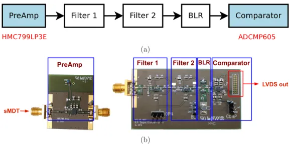
5.3. A Discrete Pulse Shaper for sMDT Tubes (ASBC)
In order to test and understand the application of baseline restoration for the sMDT read- out, a shaping circuit with properties similar to the ASD has been designed. It is called ASBC - Amplifier, Shaper, Baseline-Restorer, Comparator.
The design was carried out according to the gain of the ASD shaper stages DA 2 and
DA 3, the gain of preamp and DA 1 were approximated to be constant. The relevant
frequency range has been defined with 2 MHz to 100 MHz, according to the parameters
of a typical muon pulse ( ∼ 10 ns rise time and ∼ 500 ns fall time, see Fig. 4.11).
Time [ns]
0 100 200 300
Signal [V]
0 0.2 0.4 0.6 0.8
A
1A
2= 1.0021 A
1A
2(a)
Time [ns]
0 100 200 300
Signal [V]
0 0.5 1
A
1A
2= 0.968 A
1A
2(b)
Figure 5.6.: ASD δ-response (8 ns rise time, shaped on 1.2 pF) for (a) 50 mV and (b) 100 mV amplitude obtained from [47]. Due to the bipolar shaping scheme, the area below over- and undershoot are approximately equal. The signal amplitudes indicate the non-linearity of DA 3 (twice the input does not lead to twice the output).
5.3.1. The ASBC Circuit
The structure and a photograph of the ASBC are shown in Fig. 5.7a and 5.7b. For the sMDT signal amplification, a transimpedance amplifier
6with 10 kΩ transimpedance
7and 700 MHz bandwidth is used, corresponding to the combination of the pre-amplifier and DA 1 of the ASD. The signal shaping is conducted in three stages, where the first one does ion tail cancellation, the second one additionally shapes and differentiate the signal and the third one restores the baseline. The resulting amplified and shaped signal is then digitised, using a comparator
8with 1.6 ns propagation delay with 1 ps rms random jitter.
The voltage on the second input of the comparator can be modified to gain an adjustable signal threshold.
5.3.1.1. Filter Stage 1
The schematic of the filter stage 1 (purpose ion tail cancellation, corresponding to DA 2 of ASD) is shown in Fig. 5.8. The circuit consists of a voltage divider, which is also used for cable termination, and an AC-coupled inverting amplifier, where a pole-zero network is used as input resistor of the inverter.
5
SPICE (Simulation Program with Integrated Circuit Emphasis) implementation of Linear Technology.
6
HMC799LP3E, Hittite Microwave Corporation (PreAmp), see [48].
7
A transimpedance amplifier is a current-to-voltage converter (inverted). Therefore, the gain g is described with g =
UI= [Ω].
8
ADCMP605, Analog Devices, see [49].
(a)
(b)
Figure 5.7.: (a) Structure and (b) photograph of the ASBC (Amplifier, Shaper, Baseline- Restorer, Comparator) electronics. For sMDT signal amplification (PreAmp) a transimpedance amplifier (HMC799LP3E, see [48]) and for digitisation a comparator (ADCMP605, see [49]) is used. The pulse shaping is conducted in three stages, where the third one also restores the baseline.
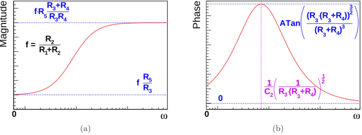
The complex resistance Z
pzof the pole-zero network is
9Z
pz(ω) = R
3k (R
4+ 1
iωC
2) (5.1)
In case of an ideal operational amplifier
10(OPA
1), a large resistance of the pole-zero network with respect to R
2and a big capacity of C
111, the complex gain G
1is calculated with
G
1(ω) = − R
2R
1+ R
2· R
5Z
pz(ω) = − R
2· R
5R
1+ R
2· (R
3+ R
4) · ωC
2− i
R
3· (R
4· ωC
2− i) . (5.2) The magnitude and phase of Eq. 5.2 are shown in Fig. 5.9a and Fig. 5.9b. While the magnitude is bounded between the limits defined by the pole-zero network, the phase show a maximum for a certain frequency (see Section A.2.5).
Eq. 5.2 describes the high-pass behaviour of the circuit, indeed, it is necessary to include the low-pass features the ASD DA2 (see Fig. 5.3a). Thus, the limited bandwidth of a real operational amplifier
12is used and the value of the feedback resistor R
5is chosen to gain the necessary bandwidth. The values of the parts shown in Fig. 5.8 are listed in Tab. A.2.
The resulting gain
13is shown Fig. 5.12. The magnitude and phase are in accordance with the corresponding ASD parameters.
9
k indicates parallel arrangement.
10
Infinite input resistance, infinite gain, infinite bandwidth
11
The capacity has to be big enough to provide AC-coupling without signal shaping.
12
For this application, THS4304 [50] is used.
13
Calculation based on the gain-bandwidth-product GBW=870 MHz (see [50]).
Figure 5.8.: Schematic of filter stage 1, see Fig. 5.7a. It consists of an AC-coupled inverting amplifier, where a pole-zero network is used as input resistor of the inverter.
Filter stage 1 is a high-pass for sMDT signal ion tail cancellation.
ω
Magnitude
R
4R
3+R
4R
3R
5⋅ f
R
3R
5f
0
+R
2R
1R
2f =
(a)
ω
Phase
21 4
)
3
+R
⋅ (R R
31 C 1
2)
3+R
4(R
32 3 4
))
3
+R
⋅ (R (R
3ATan
0 0
(b)
Figure 5.9.: Filter stage 1 magnitude (a) and phase (b) (see Eq. 5.2) depending of the frequency. The determination of the bounds is discussed in Section A.2.5.
5.3.1.2. Filter Stage 2
The schematic of the filter stage 2, which consists of a voltage divider and an inverting amplifier with an RC -circuit as input resistance, is shown in Fig. 5.10. The circuit cor- responds the differentiator shown in Fig. A.2c, its purpose is signal shaping and signal differentiation (see Eq. A.17) and its functionality corresponds to DA 3 of the ASD.
The complex resistance Z
RCof the RC-circuit is Z
RC= R
8+ 1
iωC
4, (5.3)
leading to a complex gain G
2(ω) of the circuit under the assumption of an ideal operational amplifier and a large resistance of the RC-circuit with respect to R
7G
2(ω) = − R
7R
6+ R
7· R
9Z
RC= − R
7· R
9R
6+ R
7· ωC
4ωR
8C
4− i . (5.4)
Figure 5.10.: Schematic of filter stage 2 (see Fig. 5.7a). It consists of an inverting amplifier, where an RC-circuit is used as input resistor of the inverter. Filter stage 2 is used as differentiator.
ω
Magnitude
8R R
9+R
7R
6R
70
0
(a)
ω
Phase 2 π
0
0
(b)
Figure 5.11.: Filter stage 2 magnitude (a) and phase (b) (see Eq. 5.2) versus frequency.
The determination of the bounds is discussed in Section A.2.6.
The magnitude and phase of Eq. 5.4 are shown in Fig. 5.11a and Fig. 5.11b. The circuit behaves as filter stage 1 with R
3→ ∞ in Eq. 5.2. Fig. 5.11a is Fig. 5.9a shifted and Fig. 5.11b shows the falling edge of Fig. 5.9b. In order to obtain the same gain as DA3 of the ASD (see Fig. 5.3a), low pass behaviour has to be added to filter stage 2. Thus, the amplifier bandwidth is adjusted with the feedback resistor R
9. The resulting gain is illustrated in Fig. 5.12. The magnitude shows a small difference for high frequencies of the relevant range and the phase for lower frequencies, respectively.
5.3.1.3. BLR Stage
The schematic of the BLR stage is shown in Fig. 5.13a. It uses a passive baseline restoration
concept and corresponds to the circuit shown in Fig. 5.2b, where the resistor R
10and the
inductance L
1are used together as current source and the transistor T
2is connected in a
Frequency [Hz]
104 105 106 107 108 109
Magnitude [dB]
0 5 10 15 20
25
Relevant
range Stage 1
Stage 2 ASD DA 2 ASD DA 3
(a)
Frequency [Hz]
104 105 106 107 108 109
Phase
-1.5 -1 -0.5 0 0.5 1
1.5
Relevant
range
Stage 1 Stage 2 ASD DA 2 ASD DA 3
(b)
Figure 5.12.: (a) Gain magnitude and (b) phase of stage 1 and stage 2 including the frequency behaviour (gain-bandwidth-product) of the operation amplifiers in comparison with ASD DA 2 and DA 3 , where the ASD magnitude is multiplied and the phase is shifted to reach the ASBC level.
way to act as diode. The second transistor T
2defines the current pointer and compensates the impact of small temperature changes, the capacitor C
6provides AC-coupling and R
11is a pull-down resistor defining the baseline.
The reason for using a transistor
14as diode is caused by its low capacity in comparison to commonly used diodes. Its characteristic line is shown in Fig. 5.13b. Together with C
5the transistor capacity acts as voltage divider and together with the diode as RC-circuit, so the transistor capacity should be small and C
5should be large. On the other hand, C
5affects the timing behaviour of the transistor and should be as small as possible
15. Due to the interaction of all parts, the non-linear behaviour of the diode and, hence, the shaping behaviour of the BLR stage, the parameter selection is a trade-off and the optimal values according to simulation and tests are shown in Tab. A.2.
The voltage at V
BLRdefines the current over T
1and T
2and sets, consequently, the working point. The operating principle is shown in Fig. 5.13c, the three different operating states are
• Baseline input: Due to the current flowing over R
10the diode is slightly conduct- ing, so the potential between the diodes is stable, causing the baseline at Out.
• Positive input: The positive input voltages compensates the current over R
10and shifts the diode into the non-conducting mode. If the BLR-current is small with respect to the signal current over C
5, the signal at Out is the same as at In.
• Negative input: The negative input voltage shifts the diode into the full conducting mode, causing a short-circuit of the signal to ground and, therefore, restoring the baseline.
14
The used transistor (PNP) is a BFT92, see [51].
15
For details on the timing behaviour of semi-conductors see [52].
(a)
Voltage [V]
0 0.2 0.4 0.6 0.8
A] µ Current [
0 50 100 150 200 250 300
(b)
Time
Signal
Baseline
Diode voltage
Diode current
0
Working point Diode slightly conducting
Diode voltage
Diode current
0
Positive input signal Diode non-conducting
Diode voltage
Diode current
0
Negative input signal Diode conducting
(c)
Figure 5.13.: (a) Schematic of baseline restoration stage, see Fig. 5.7a. The circuit is based on the passive BLR concept, where a transistor is used as diode due to its low capacity. The working point is defined by the voltage at V
BLR, R
10and L
1, which together act as current source.
(b) Characteristic line of BFT92 used as diode (wiring corresponding to (a)).
(c) Operating principle of the baseline-restorer shown in (a). On the working
point (baseline input), the diode is slightly conducting, for positive input
signals it become non-conducting and negative signals are drained to ground.
Time [s]
-50 0 50 100 150 200 250 300 350 400
Scaled signal [V]
-0.05 0 0.05
0.1
ASD
ASBC (no BLR current)
0 5 10 15 20 25
-0.04 -0.02 0 0.02 0.04 0.06 0.08 0.1 0.12 0.14
t = 6.1 ns
∆
Default ASD Threshold
Rise times = 11.6 ns t
ASD= 7.5 ns t
ASBCFigure 5.14.: δ-response of ASD and ASBC (scaled to fit the amplitude of the ASD re- sponse). The δ-signal was obtained by shaping a square pulse of 800 mV amplitude with 1.2 pF capacity. The right plot indicates the difference of the rise times for an ASD threshold of 38 mV.
If the working point is too low, the diode does not shift into conducting mode, if, however, it is too high, the diode never becomes non-conducting. So the working point has to be chosen with care, and the behaviour of the ASBC depending of V
BLRhas to be measured.
In this thesis, the following definitions are used:
• ASBC without BLR: The diode current is zero.
• ASBC with BLR: The diode is operated at the working point.
5.3.2. Comparison of ASD and ASBC δ-Response
In Fig. 5.14 the δ-response of ASD and ASBC without BLR measured in front of the discriminator is shown. The input pulse is obtained from an AC-coupled (1.2 pF) square signal.
There are two major differences between ASD and ASBC
• The rise time
16of the ASBC is smaller.
• The bipolar undershoot is smaller and faster.
The smaller rise time which is caused by higher bandwidth of the ASBC electronics PreAmp (the ASD chip Preamp and DA 1 are part of the signal shaper, see Section 5.2) is expected to have a positive impact on resolution and efficiency, because the faster rising edge minimises the time-slewing effect. Likewise, the signal pile-up effect for high counting rates is expected to be suppressed.
In addition, further pile-up suppression by the smaller bipolar undershoot is expected.
16
Time between 10% and 90% of the signal amplitude.
Time
Signal
t
fallt
riseU
maxFigure 5.15.: Parametrisation of input pulse with rise time (t
rise), fall time (t
f all) and amplitude (U
max). Due to AC-coupling of the shaping circuit, the absolute level of the baseline does not matter and the difference between baseline and peak is the relevant parameter.
5.3.3. ASBC Response for a Parametrised Pulse
The first approach to evaluate the behaviour of baseline restoration implementation is the ASBC response measured in front of the comparator for a simplified pulse representing the actual muon and background caused pulses.
In Fig. 5.15 the pulse shape, which is a δ-pulse with different rise and fall time, used for the following measurements is shown. The three pulse parameters are the amplitude U
max, the rise time t
riseand the fall time t
f all. Due to AC-coupling of the shaping circuit, the absolute level of the baseline does not matter and the difference between baseline and peak is the relevant parameter.
Due to its high bandwidth with respect to the shaper, the ASBC pre-amplifier has no shaping effect on the signals. Hence, the following measurements were obtained from the ASBC without pre-amplifier.
In Fig. 5.16 the response for different BLR currents is shown. The BLR current has impact on the amplitude as well as on the undershoot. Following the diode characteristic line shown in Fig. 5.13b, the undershoot suppression increases with the BLR working point until a certain current value. The value is the optimal working point. As soon the working point is set in the linear range of the diode, further suppression of the bipolar undershoot with respect to the response amplitude is not possible.
In Fig. 5.17a the amplitude and in Fig. 5.17b the recovery time
17of the ASBC response depending on the working point for different input pulse amplitudes are shown. These measured functions can be explained with the diode threshold and characteristic line. As soon the working point is above the diode threshold, the BLR impact increases until a certain value. Fig. 5.17b shows that the optimal working point is approximately 90 µA.
17
![Figure 3.2.: Cut-away view of the ATLAS Muon Spectrometer. RPCs and TGCs are used as trigger chambers, CSCs and MDTs are used for precision measurement [9].](https://thumb-eu.123doks.com/thumbv2/1library_info/4014243.1541300/15.892.134.757.151.615/figure-atlas-muon-spectrometer-trigger-chambers-precision-measurement.webp)
![Figure 3.4.: Schematic overview of the trigger and DAQ system for collision data taking operations [12] (see text).](https://thumb-eu.123doks.com/thumbv2/1library_info/4014243.1541300/17.892.157.740.151.526/figure-schematic-overview-trigger-daq-collision-taking-operations.webp)
![Figure 4.5.: Block diagram of the on-chamber data processing with Mezzanine boards, CSM, ELMB, TTC, and MROD [21]](https://thumb-eu.123doks.com/thumbv2/1library_info/4014243.1541300/24.892.138.766.149.519/figure-block-diagram-chamber-processing-mezzanine-boards-elmb.webp)
![Figure 4.6.: Drift-time spectra of MDT and sMDT tubes operated with Ar:CO2 (93:7) gas mixture at 3 bar absolute pressure and a gas gain of 20000 [25]](https://thumb-eu.123doks.com/thumbv2/1library_info/4014243.1541300/25.892.192.698.148.504/figure-drift-spectra-tubes-operated-mixture-absolute-pressure.webp)
![Figure 5.4.: Block diagram of one channel of the ASD chip consisting of four stages [22]](https://thumb-eu.123doks.com/thumbv2/1library_info/4014243.1541300/35.892.176.720.152.377/figure-block-diagram-channel-asd-chip-consisting-stages.webp)