https://doi.org/10.1007/s00706-020-02635-0 ORIGINAL PAPER
A cost‑efficient approach for simultaneous scanning electrochemical microscopy and scanning ion conductance microscopy
Stefan Wert
1· Simona Baluchová
2· Karolina Schwarzová‑Pecková
2· Silvia Sedláková
3· Andrew Taylor
3· Frank‑Michael Matysik
1Received: 27 March 2020 / Accepted: 2 June 2020 / Published online: 17 June 2020
© The Author(s) 2020
Abstract
A novel and cost-efficient probe fabrication method yielding probes for performing simultaneous scanning electrochemi- cal microscopy (SECM) and scanning ion conductance microscopy (SICM) is presented. Coupling both techniques allows distinguishing topographical and electrochemical activity information obtained by SECM. Probes were prepared by deposi- tion of photoresist onto platinum-coated, pulled fused silica capillaries, which resulted in a pipette probe with an integrated ring ultramicroelectrode. The fabricated probes were characterized by means of cyclic voltammetry and scanning electron microscopy. The applicability of probes was demonstrated by measuring and distinguishing topography and electrochemi- cal activity of a model substrate. In addition, porous boron-doped diamond samples were investigated via simultaneously performed SECM and SICM.
Graphic abstract
Keywords Electrochemistry · Redox reactions · Cyclic voltammetry · Scanning electrochemical microscopy · Scanning ion conductance microscopy · Boron-doped diamond
Introduction
Scanning electrochemical microscopy (SECM) is a power- ful technique for the investigation of electrochemical and topographical properties of surfaces [1]. It belongs to the family of scanning probe techniques and features small electrodes as probes with electroactive diameters of 25 µm or less, which are termed ultramicroelectrodes (UMEs).
Measurements are usually performed in a solution contain- ing a reversible redox-active species, the so-called redox mediator. In the amperometric mode of SECM, a constant potential is applied to the UME, leading to the conversion of the mediator associated with a faradaic current that can be recorded. As the probe is scanned over the surface of a
Electronic supplementary material The online version of this article (https ://doi.org/10.1007/s0070 6-020-02635 -0) contains supplementary material, which is available to authorized users.
* Frank-Michael Matysik
frank-michael.matysik@chemie.uni-regensburg.de
1 Institute of Analytical Chemistry, Chemo- and Biosensors, University of Regensburg, Regensburg, Germany
2 UNESCO Laboratory of Environmental Electrochemistry, Department of Analytical Chemistry, Faculty of Science, Charles University, Prague, Czech Republic
3 FZU-Institute of Physics of the Czech Academy of Sciences, Prague, Czech Republic
be utilized [4]. For this technique, a small micropipette is employed as a probe. As it is filled with supporting electro- lyte and has a quasi-reference electrode placed within the interior of the pipette, a potential can be applied between the inner electrode and another quasi-reference electrode located in the bulk solution of the measurement cell. This results in an ionic current flowing between the pipette interior and the surrounding solution. Moving the pipette close to the surface leads to hindered ion migration at the pipette orifice, which is manifested by increased resistance and thus, lower current.
Performing SECM and SICM measurements simultane- ously enables distinguishable acquisition of topographical and electrochemical activity information on surfaces. For the hyphenation of both techniques, probes with an integrated UME for SECM and a channel with micro- or nanometer size for SICM are required. To date, various approaches for the fabrication of such probes exist. Initial approaches were carried out by Hersam et al. [5] by depositing gold on one side of a nanopipette followed by isolation with Al
2O
3, both applied via atomic layer deposition. Another method fea- tures sputtering to create a noble metal surface and isolat- ing the outer surface with electrophoretic paint [6]. Popular means for the fabrication of the UME part of probes feature pyrolysation of butane gas [7–9] or parylene C [10] to cre- ate carbon electrodes. The latter has also been used as an insulating material [10, 11]. Alternatively, pulled theta (dual barrel) capillaries were employed as housing of the probe and one barrel was filled with pyrolytic carbon as mentioned above, yielding a carbon barrel for SECM and an empty barrel for SICM. The latter was filled with electrolyte and a Ag/AgCl wire prior to measurements. In all dual-probe fabrication techniques mentioned before, focused ion beam milling is usually utilized to expose the electrode surface.
These probes have recently been applied to the investiga- tion of hydrogen peroxide generation at gold nanoparticles [12] and the surface characterization of different cells [9, 13]. Single-barrel nanopipette probes with electrode mate- rial deposited around the orifice have been realized with the
ods require sophisticated equipment, we aimed to develop a novel and cost-efficient approach for the preparation of such probes. The fabricated probes were characterized by scan- ning electron microscopy (SEM) and cyclic voltammetry (CV), revealing information about their size and functional- ity. The response in SECM and SICM probe approach curves (PACs) towards gold and glass surfaces was tested as well.
Eventually, separate images showing the electrochemical activity and morphology of a model substrate and a porous BDD sample were recorded.
Results and discussion
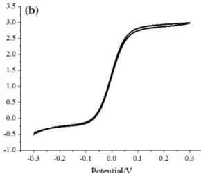
The quality of the coating of the fabricated ring UME pipette probes was investigated by means of CV. Figure 1a shows a CV recorded with a probe being coated six times with a pho- toresist solution according to the procedure described in the experimental section. Subsequent polishing yielded a probe with a ring diameter of 25 µm. Figure 1b depicts the corre- sponding CV. The oxidation currents measured in both cases correspond well to ring UME theory [17] for electrodes with ring diameters of 2 µm and 25 µm, respectively. Based on microscopical studies and evaluation of recorded CVs and according to the theory of ring UME voltammetry [17], a thickness of the platinum film of < 50 nm can be estimated for both polished and unpolished probes.
To investigate the response of the probes approaching
conducting and non-conducting surfaces, PACs towards
gold and polymer on a model substrate were performed. In
Fig. 2a, the SECM feedback curves of a 25-µm ring diam-
eter probe approaching both conductor (gold) and isolator
(polymer) are displayed. The typical positive and negative
feedback responses were found. For SICM, a response-inde-
pendent conductivity was expected. The corresponding PAC
is shown in Fig. 2b. Approaching the surface resulted in
initially slowly decreasing current, possibly due to potential
shift during the measurement. Nevertheless, when substrate-
to-tip distance similar to the pipette aperture radius was
reached, the current decreased drastically due to hindered ion migration between pipette interior and bulk solution.
Overall, the approach responses indicated proper functional- ity of the dual probes.
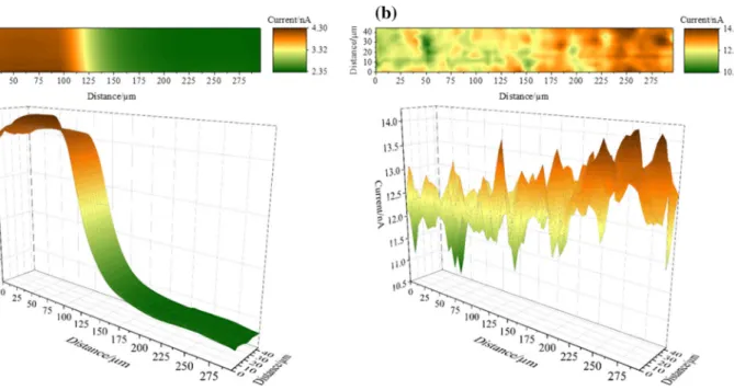
Images of the screen-printed model substrate were recorded to test the capability of the fabricated probes to perform simultaneous local topographical and conductiv- ity studies. Figure 3 shows the SECM (a) and SICM (b) responses at the edge of the conductive electrode area. The SECM image clearly shows a sharp current transition from the conducting gold area in the left half of the image to the insulating polymer in the right half, as positive and negative feedback were measured on the left and right side, respec- tively. The SICM response indicates a significant roughness over the entire area of the sensor. In addition, overall current increase from the conducting to the insulating area shows
that the sensor is thicker at the electrode area, since the elec- trode material was printed onto the polymer carrier. Both observations could be confirmed by digital micrographs (included in Supporting information Fig. S1).
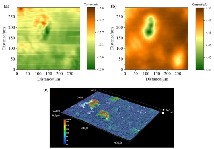
Furthermore, the fabricated SECM–SICM probes were utilized to investigate a porous BDD sample regarding its electrochemical surface properties in relation to topography.
In Fig. 4a, the SECM image showing overlapping electro- chemical and topographical information is presented. Loca- tions exhibiting higher currents indicated either the occur- rence of higher electrochemical activity or topographical extrusion of the surface. To differentiate between these two types of information, the SICM image displayed in Fig. 4b can be utilized, covering the same area previously investi- gated via SECM. Herein, low current areas as a result of a small substrate-to-tip distance indicate the presence of
Fig. 1 Cyclic voltammograms (CVs) a with an unpolished pipette probe with a ring OD of 2 µm, b with a polished pipette probe with a ring OD of 25 µm. Scan rate: 20 mV s−1. A Pt wire served as quasi-
reference/counter electrode in a solution containing 1.5 mmol dm−3 FcMeOH and 0.2 mol dm−3 KNO3
Fig. 2 Probe approach curves (PACs) of a 25 µm OD dual SECM/SICM probe. a SECM PACs, approaching platinum (conductor, red) and insu- lating polymer (insulator, black). E (Probe) = + 0.3 V b SICM PAC. E (Probe) = + 0.2 V (color figure online)
topographical elevation. Digital micrographs of the sample, shown in Fig. 4c, support these observations. Extrusions generally occur in the same locations where the high current was observed in the SECM image. Nevertheless, deviations were noticeable, as areas exhibiting both low electrochemi- cal activity and topological extrusions occurred as well.
Therefore, variations in the SECM might be caused by both inhomogeneous topography and porosity of the sample, in addition to electrochemical differences. The latter is possibly a consequence of non-uniform distribution of boron doping ratio within the BDD layer. Similar observations were made for nonporous BDD samples [24].
Conclusion
A new approach for the fabrication of probes suitable for simultaneous SECM and SICM measurements was devel- oped and functional probes of different size were success- fully manufactured. In addition, the materials and instru- ments required for the preparation of probes are cost efficient and easy to acquire. The probes were characterized via CV, SEM images, and PACs towards isolating and conducting surfaces. Electrochemical and topographical variations at a model substrate surface as well as a porous BDD sample could be resolved. The probe preparation concept suggested in this work facilitates the widespread use of combined SECM and SICM as a means for simultaneous non-contact
topographical and electrochemical activity studies of surfaces.
Experimental
All experiments were carried out with ferrocenemeth- anol (c = 1.5 mmol dm
−3, FcMeOH, 99%, ABCR, Karlsruhe, Germany) or hexaamineruthenium(III) chlo- ride (c = 1.5 mmol dm
−3, Ru(NH
3)
6Cl
3, ABCR, Karlsruhe, Germany) as a redox mediator. To prepare aqueous solu- tions, Milli-Q water (Milli-Q Advantage A10 system, Merck Millipore, Darmstadt, Germany) was used. KNO
3(c = 0.2 mol dm
−3, analytical grade, Merck KGaA, Darm- stadt, Germany) and KCl (c = 0.2 mol dm
−3, analytical grade, Merck KGaA, Darmstadt, Germany) served as sup- porting electrolytes. A 10:1 mixture of SU8.5 photoresist (MicroChem Corp., Westborough, Massachusetts) and ethanol (Merck Millipore, Burlington, Massachusetts) was utilized for preparing isolating coatings.
Instrumentation
Probes were fabricated by modifying platinum-coated emitters for electrospray ionization (New Objective, Woburn, Massachusetts). The fabrication protocol is illustrated in Fig. 5. Initially, the capillaries were pushed
Fig. 3 a Electrochemical activity (SECM) and b topographical (SICM) images of an electrochemical sensor substrate obtained via simultaneous SECM and SICM recordings. 2D (top) and 3D (bottom) projections are shown. An area of 45 × 300 µm was investigated, cov-
ering the edge of the working electrode pad of the sensor. E (Probe, SECM) = + 0.3 V. E (Probe, SICM) = + 0.2 V. Scan rate: 40 µm s−1. Quiet time: 10 s
through a copper tube (1.1 mm ID, 2.0 mm OD, 3.0 cm length, Albion Alloys, Bournemouth, United Kingdom) for establishing electrical contact to the platinum surface of the probes. Contact between copper and platinum was established using silver conductive paint (VS Electronic, Aschaffenburg, Germany) and adhesive (UHU Max Repair Extreme, UHU GmbH & Co. KG, Bühl, Germany). After- wards, a photoresist solution was applied under N
2flow, cured by UV light (350 nm, applied for 30 s) and heated in an oven at 95 °C for 5 min to evaporate the remaining solvent. The quality of the coating was investigated by
CV and the coating process was repeated if the measured currents were too high. If larger probes were desired, an alternative way to expose a ring electrode surrounding was applied. The tips were polished with alumina lapping sheets (0.3 μm, Precision Surfaces International, Houston, Texas), while water was flushed through the pipette to pre- vent clogging.
Eventually, probes were filled with supporting electrolyte and a Ag/AgCl wire was inserted. Figure 6a shows a typical example of a finished tip. The individual layers of the probe tip are schematically shown in Fig. 6b. An image of the
Fig. 4 a SECM and b SICM images of a porous BDD sample, recorded simultaneously. An area of 294 × 294 µm was scanned.
Increment distance: 3 µm; mediator for SECM: Ru(NH3)6Cl3; E (Probe, SECM) = − 0.4 V. E (Substrate, SECM) = 0 V. E (Probe,
SICM) = + 0.2 V. Scan rate: 30 µm s−1. Quiet time: 60 s. c Optical micrograph of a porous BDD sample showing the topographical char- acteristics
Fig. 5 Probe fabrication scheme. To obtain a functional probe, multiple layers had to be applied or the tip needed to be polished
Japan) is depicted in Fig. 6c.
Experiments with the fabricated probes were performed with a second Ag/AgCl wire placed in the bulk solution employed as both counter and reference electrode for SECM measurements. The mentioned potentials herein refer to this reference system if not stated otherwise.
Measurements were performed using a commercially available SECM 920C (CH Instruments, Austin, Texas), with the first electrode channel being connected to the inter- nal Ag/AgCl wire of the ring UME pipette for recording the SICM current and the second channel connected to the copper tube for measuring the SECM current.
The approach response of the fabricated probes was investigated by performing PACs over both gold and poly- mer of a screen-printed electrochemical sensor (Fig. 7a, b, GlucoSmart® Swing, MSP bodmann GmbH, Germany) as conductive and non-conductive surfaces, respectively.
A potential of + 0.3 V (SECM) was applied and the probe was approached until the SECM current increased to 135%
(conductor) or decreased to 85% (insulator) with respect to the current measured in bulk solution. In addition, a quiet
rate was set to 1.25 µm s
−1.
For simultaneous SECM and SICM measurements, the contact pads of the same sensor served as a model sub- strate. Its roughness and the transition between conducting and insulating surface were investigated. Potentials of + 0.3 (SECM) and + 0.2 V (SICM) were applied and FcMeOH served as a redox mediator. The scan rate of the probe was 40 µm s
−1with a pixel size of 4 µm.
Porous BDD samples were deposited on conductive p-Si wafers with a planar BDD base layer using an ASTeX 5010 (Seki Technotron, Japan) deposition system under the fol- lowing conditions: 0.5% of methane in hydrogen, gas pres- sure equal to 50 mbar, microwave power of 1150 W, and substrate temperature of ca. 750 °C. Boron doping was car- ried out by the addition of trimethylboron in the gas phase to give a B/C ratio of 4000 ppm. Porous BDD samples were obtained by two-step diamond deposition (a growth dura- tion of each step was 5 h) on a ca. 4–5 μm thick 3D template comprising of nanodiamond seeded SiO
2nanofibers in a polymer solution, which was spin coated (at 3000 rpm for 30 s) on top of a planar BDD base layer and then dried on
Fig. 7 a Image of the electrochemical sensor used as a model sub- strate. b Zoomed view of the electrode pads of the glucose sensor with the area investigated by means of SECM/SICM highlighted in
yellow. c BDD sample mounted onto a sample holder. d BDD sam- ple with sample holder mounted in the electrochemical cell used for measurements (color figure online)
a hot plate (110 °C/90 s). The surface of fabricated porous BDD samples was hydrogen terminated (as-grown).
The BDD samples were mounted onto a substrate holder prior to measurements (Fig. 7c), enabling a well-defined potential setting of the BDD sample. The sample holder con- sisted of a brass rod sealed with polyvinyl chloride (brass diameter: 3 mm, outer diameter of the polyvinyl chloride hollow cylinder: 6.5 mm, fabricated by the mechanical work- shop of the University of Regensburg), with the rod exceed- ing on one end to facilitate electrical contact and another flat end where porous BDD samples were mounted. Electrical contact between porous BDD and brass rod was established by applying silver conductive paint on the rod and placing the porous BDD sample on top. After drying at room tem- perature for 1 h, the gap between rod and sample was sealed with epoxide resin (UHU plus endfest 300, UHU GmbH
& Co. KG, Bühl, Germany). After hardening of the resin, which required 24 h, the remaining gaps were filled with epoxy resin as before. Excess resin was removed by carefully polishing the edges of the sample with abrasive paper (grit size 100) until the sample fit into the electrochemical cell shown in Fig. 7d. Porous BDD samples were measured with Ru(NH
3)
6Cl
3as a mediator, applying 0.0 V to the substrate and − 0.4 and + 0.2 V to the SECM and SICM parts of the probe, respectively. An area of 294 × 294 µm was investi- gated at a scan rate of 30 µm s
−1and a pixel size of 3 µm.
Initial surface studies of the samples were performed with a digital microscope (VHX-7000, Keyence, Osaka, Japan).
Acknowledgements Open Access funding provided by Projekt DEAL.
This research was carried out within the framework of Specific Univer- sity Research (SVV 260440). S.B. gratefully acknowledges financial support provided by the Grant Agency of Charles University (project no. 390119). The authors would like to thank Thomas Herl for the help with designing schemes and the graphical abstract.
Open Access This article is licensed under a Creative Commons Attri- bution 4.0 International License, which permits use, sharing, adapta- tion, distribution and reproduction in any medium or format, as long as you give appropriate credit to the original author(s) and the source, provide a link to the Creative Commons licence, and indicate if changes were made. The images or other third party material in this article are included in the article’s Creative Commons licence, unless indicated otherwise in a credit line to the material. If material is not included in the article’s Creative Commons licence and your intended use is not permitted by statutory regulation or exceeds the permitted use, you will need to obtain permission directly from the copyright holder. To view a copy of this licence, visit http://creat iveco mmons .org/licen ses/by/4.0/.
References
1. Bard AJ, Mirkin MV (eds) (2012) Scanning electrochemical microscopy, vol 2. CRC Press, Boca Raton
2. Macpherson JV, Unwin PR (2000) Anal Chem 72:276
3. Velmurugan J, Agrawal A, An S, Choudhary E, Szalai VA (2017) Anal Chem 89:2687
4. Hansma PK, Drake B, Marti O, Gould SA, Prater CB (1989) Sci- ence 243:641
5. Comstock DJ, Elam JW, Pellin MJ, Hersam MC (2010) Anal Chem 82:1270
6. Takahashi Y, Shevchuk AI, Novak P, Murakami Y, Shiku H, Korchev YE, Matsue T (2010) J Am Chem Soc 132:10118 7. Takahashi Y, Shevchuk AI, Novak P, Zhang Y, Ebejer N,
Macpherson JV, Unwin PR, Pollard AJ, Roy D, Clifford CA, Shiku H, Matsue T, Kleneman D, Korchev YE (2011) Angew Chem Int Ed Engl 50:9638
8. O’Connell MA, Wain AJ (2014) Anal Chem 86:12100
9. Page A, Kang M, Armitstead A, Perry D, Unwin PR (2017) Anal Chem 89:3021
10. Thakar R, Weber AE, Morris CA, Baker LA (2013) Analyst 138:5973
11. Morris CA, Chen C-C, Baker LA (2012) Analyst 137:2933 12. O’Connell MA, Lewis JR, Wain AJ (2015) Chem Commun
(Camb) 51:10314
13. Takahashi Y, Kumatani A, Shiku H, Matsue T (2017) Anal Chem 89:342
14. Szabo A (1987) J Phys Chem 91:3108
15. Walsh DA, Fernández JL, Mauzeroll J, Bard AJ (2005) Anal Chem 77:5182
16. Cornut R, Mayoral M, Fabre D, Mauzeroll J (2010) J Electrochem Soc 157:F77
17. Lee Y, Amemiya S, Bard AJ (2001) Anal Chem 73:2261 18. Muzyka K, Sun J, Fereja TH, Lan Y, Zhang W, Xu G (2019) Anal
Methods 11:397
19. Baluchová S, Daňhel A, Dejmková H, Ostatná V, Fojta M, Schwarzová-Pecková K (2019) Anal Chim Acta 1077:30 20. Zanin H, May PW, Fermin DJ, Plana D, Vieira SMC, Milne WI,
Corat EJ (2014) ACS Appl Mater Interfaces 6:990
21. Baluchová S, Taylor A, Mortet V, Sedláková S, Klimša L, Kopeček J, Hák O, Schwarzová-Pecková K (2019) Electrochim Acta 327:135025
22. Holt KB, Bard AJ, Show Y, Swain GM (2004) J Phys Chem B 108:15117
23. Ryl J, Burczyk L, Zielinski A, Ficek M, Franczak A, Bogdanowicz R, Darowicki K (2019) Electrochim Acta 297:1018
24. Neufeld AK, O’Mullane AP (2006) J Solid State Electrochem 10:808
Publisher’s Note Springer Nature remains neutral with regard to jurisdictional claims in published maps and institutional affiliations.