Development and application of an experimental concept for surface characterization of semiconductor
based substrates using scanning electrochemical microscopy
Dissertation
Zur Erlangung des Doktorgrades der Naturwissenschaften (Dr. rer. nat.) der Fakultät für Chemie und Pharmazie
der Universität Regensburg vorgelegt von Patrick Hanekamp
aus Laaber im Jahr 2018
Die vorgelegte Dissertation entstand in der Zeit von März 2016 bis September 2018 am Institut für Analytische Chemie, Chemo- und Biosensorik der naturwissenschaftlichen Fakultät IV- Chemie und Pharmazie - der Universität Regensburg.
Die Arbeit wurde angeleitet von: Prof. Dr. Frank Michael-Matysik.
Das Promotionsgesuch wurde eingereicht am: 17. Dezember 2018
Termin des Kolloquiums: 15.03.2019
Dem Prüfungsausschuss saß Prof. Dr. Alkwin Slenczka vor. Erstgutachter war Prof. Dr. Frank-Michael Matysik, Zweitgutachter war Prof. Dr. Alfred Lechner und Drittprüfer war Prof. Dr. Arno Pfitzner.
List of content
List of content ... I Oral and poster presentations ... III List of publications ... IV Declaration of collaboration ... VII List of abbreviations ... VIII
1 Introduction ... 1
2 Theory ... 5
2.1 Voltammetry... 5
2.1.1 Fundamentals of voltammetry ... 5
2.1.2 Mass transfer towards the electrode surface ... 9
2.1.3 Voltammetric behavior of macroelectrodes and microelectrodes ... 11
2.1.4 Voltammetric techniques ... 15
2.2 Scanning electrochemical microscopy ... 19
2.2.1 Measurement setup of scanning electrochemical microscopy ... 19
2.2.2 Electrochemical mediators ... 20
2.2.3 Working modes in scanning electrochemical microscopy ... 21
2.2.4 Imaging process ... 26
2.3 Electrochemical deposition of copper ... 27
2.3.1 Electroplating of copper in semiconductor industry ... 27
2.3.2 Barrier films for copper ... 30
2.3.3 Nucleation process ... 32
2.3.4 Electrochemical deposition of copper on barrier films ... 35
3 Experimental ... 48
3.1 Materials ... 48
3.2 Mediators ... 50
3.3 Copper electrolytes ... 51
3.4 SECM probe fabrication and characterization ... 52
3.4.1 Fabrication of ultramicroelectrodes ... 52
3.4.2 Characterization of ultramicroelectrodes ... 53
3.5 Multipurpose cell... 55
4 Results and discussion ... 58
4.1 Development and application of a multipurpose electrodeposition cell configuration ... 58
4.1.1 Introduction ... 59
4.1.2 Experimental ... 60
4.1.3 Result and discussion ... 63
4.1.4 Conclusion ... 68
4.2 Probe approach curves on barrier films on semiconductor substrates ... 73
4.2.1 Introduction ... 73
4.2.2 Experimental ... 74
4.2.3 Result and discussion ... 75
4.2.4 Conclusion ... 80
4.3 Material contrast studies of conductive thin films on semiconductor substrates using scanning electrochemical microscopy ... 83
4.3.1 Introduction ... 84
4.3.2 Experimental ... 85
4.3.3 Result and discussion ... 89
4.4 Nucleation studies on ruthenium from various electrolytes ... 102
4.4.1 Introduction ... 102
4.4.2 Experimental ... 103
4.4.3 Result and discussion ... 106
4.4.4 Conclusion ... 113
5 Summary... 116
6 Zusammenfassung in deutscher Sprache ... 118
Oral and poster presentations
Oral presentations
1st Cross-Border Seminar on Electroanalytical Chemistry (ELACh), 4.-6. April 2018, Furth im Wald, Germany
Multipurpose electrochemical cell concept: Surface modification and characterization of semiconductor substrates
Scanning electrochemical microscopy (SECM) is a unique scanning probe method to study samples like coatings, electrodes and membranes in liquid environments. With this technique the electrochemical reactivity and the topography of the substrate can be measured by scanning the probe across the surface.
Therefore SECM is a promising technique for the investigation of the electrochemical deposition of copper onto metallic barrier materials or the density of barrier films on semiconductor substrates.
In the frame of this contribution a versatile experimental cell configuration for semiconductor thin film materials is presented [1]. This multipurpose cell setup is designed to conduct semiconductor plating processes in laboratory scale and also to characterize the electrochemical activity of the surface with SECM. For this purpose the silicon substrates with the thin-film barrier materials are placed in a special sample holder ensuring electrical contact of the sample surface with a small circular area of 16 mm² exposed to the electrolyte solution.
The multipurpose electrochemical cell configuration was used to obtain information concering film coalescences, grainsize and growth mode during potentiostatic copper deposition on thin-film ruthenium.
In addition, thin film copper, titanium, and silicon nitride are studied with SECM concerning their local electrochemical activity. The gained results indicate that biasing of the substrate is essential for non- destructive and interaction-free measurements of semiprecious films and structures in the case of ferrocenemethanol mediator solution.
Literature:
[1] Hanekamp P, Robl W, Matysik F-M (2017) J. Appl. Electrochem.47(12):1305-1312
Poster presentations
Electrochemistry 2016, 26.-28.9.2016, Goslar, Germany
Characterisation of barrier materials on semiconductor substrates by means of scanning electrochemical microscopy
Patrick Hanekamp and Frank-Michael Matysik
ANAKON 2017, 3.-6.4.2017, Tübingen
Characterisation of barrier materials on semiconductor substrates by means of scanning electrochemical microscopy
Patrick Hanekamp and Frank-Michael Matysik
List of publications
Peer reviewed articles
Development and application of a multipurpose electrodeposition cell configuration Patrick Hanekamp, Werner Robl and Frank-Michael Matysik,
Journal of Applied Electrochemistry 47 (2017): 1305-1312.
Abstract
In this report a versatile experimental concept for electrochemical deposition and subsequent surface characterization studies is presented. This concept can be utilized to perform semiconductor plating processes at laboratory scale followed by scanning electrochemical microscopy (SECM). The same sample holder used for electroplating experiments could be integrated into the SECM instrument. Conductive thin-film barrier materials were deposited on planar silicon wafers. The substrate samples were fixed in the multipurpose sample holder ensuring a large electrical contact area to minimize ohmic drop across the sample surface with a small circular area of the substrate material of 16 mm² exposed to electrolyte solution. In order to investigate the capabilities of the electrochemical cell configuration, a potentiostatic copper deposition on ruthenium was carried out. Thus, information on film coalescences, grainsize and
growth mode could be derived. SECM was used to study the effect of biasing during probe approach curves on a titanium surface. Furthermore, microstructured copper layers were imaged using ferrocenemethanol (FcMeOH) as mediator. The results show that biasing the substrate is essential for nondestructive and interaction-free measurements of semiprecious thin-film materials and copper structures, if FcMeOH is used as electrochemical mediator.
Material contrast studies of conductive thin films on semiconductor substrates using scanning electrochemical microscopy
Patrick Hanekamp, Timo Raith, Christian Iffelsberger, Tobias Zankl, Werner Robl and Frank-Michael Matysik
Journal of Applied Electrochemistry (2019): 1-9 Abstract
In this paper a mediator-free scanning electrochemical microscopy (SECM) imaging concept is presented, which is capable of generating high electrochemical contrast and high spatial resolution between two conductive materials. The methodical approach is based on the hydrogen evolution reaction which shows potential dependent material selectivity. Various conductive thin films deposited on silicon substrates were studied. The investigated materials included copper, ruthenium, platinum, tantalum nitride, and titanium nitride. The hydrogen evolution was studied with chronoamperometry (Esubstrate = -1 V vs.
Ag/AgCl/3 M KCl) to characterize the material selectivity of this reaction for the above listed thin films.
SECM imaging in the substrate generation-tip collection (SG/TC) mode was carried out and applied to study the boundary regions of thin copper films in combination with the aforementioned thin film materials. In addition, the spatial resolution of hydrogen based SG/TC SECM imaging was characterized using lithographically fabricated platinum/copper structures as test substrates. For comparison, the common feedback mode was also applied for SECM imaging of the conducting thin film combinations. It was found, that only the hydrogen based SG/TC mode enabled SECM imaging with clear material contrast between different conductive materials which was not possible in the feedback mode.
Non-Peer reviewed articles
Trends in der elektrochemischen Rastermikroskopie
Christian Iffelsberger, Timo J. Raith, Patrick J. Hanekamp, Preety Vatsayayan und Frank- Michael Matysik, chrom+food FORUM 4 (2017) 20-22
Declaration of collaboration
The majority of the theoretical and practical research of the presented work was created by the author alone. However, some of the obtained results were achieved in cooperation with other researchers. In accordance with § 8 Abs. 1 Satz 2 Punkt 7 of the Ordnung zum Erwerb des akademischen Grades eines Doktors der Naturwissenschaften (Dr. rer. nat.) an der Universität Regensburg vom 18. Juni 2009, this section describes the nature of these collaborations. In the following, the proportion of these cooperations are specified in dependence of their appearance in the chapter sequence.
4.1 Development and application of a multipurpose electrodeposition cell configuration
SECM measurements, electroplating experiments and the theoretical work were performed by the author.
SEM images were taken by Walter Früchtl. Thin film samples on wafer specimen were provided by Infineon Technologies AG. Werner Robl and Frank-Michael Matysik were involved in discussions.
4.2 Probe approach curves on barrier films on semiconductor substrates
Experiments were performed solely by the author. Thin film samples on wafer specimen were provided by Infineon Technologies AG. Some of the obtained results are published in: Material contrast studies of conductive thin films on semiconductor substrates using scanning electrochemical microscopy (submitted for publication). Christian Iffelsberger, Frank-Michael Matysik and Werner Robl were involved in the discussions.
4.3 Material contrast studies of conductive thin films on semiconductor substrates using scanning electrochemical microscopy
Experiments were performed solely by the author. Thin film samples on wafer specimen were provided by Infineon Technologies AG. Fabrication of lithographically structured thin films was done by Tobias Zankl.
The artwork of the graphical abstract was done in cooperation with Thomas Herl. Timo Raith, Christian Iffelsberger, Frank-Michael Matysik and Werner Robl were involved in the discussions. Furthermore, Timo Raith was involved in the writing process.
4.4 Nucleation studies on ruthenium from various electrolytes
Electroplating experiments and interpretation were done by the author. Thin film samples on wafer specimen were provided by Infineon Technologies AG. SEM images were recorded by Daniel Fruechtl.
Werner Robl was involved in discussions.
List of abbreviations
A a) Area [m2]
b) Accelerator
A’ Nucleation rate constant [s-1]
ACu% Copper surface coverage [%]
Adep Area of deposition [m2]
ALD Atomic layer deposition
c Concentration [mol l-1]
c0 Bulk concentration [mol l-1]
CDL Capacity of the double layer [F]
CE Counter electrode
D Diffusion coefficient [cm2 s-1]
dcoal Layer thickness of coalescence [µm]
dinner Inner diameter [m]
DO Diffusions coefficient of oxidized species [cm2 s-1]
douter Outer diameter [m]
DR Diffusions coefficient of reduced species [cm2 s-1]
E Potential [V]
e- Electron
ECD Electrochemical deposition
Eeff Effective applied potential [V]
F Faraday constant 9.64853104 C mol-1
FcMeOH Ferrocenemethanol
HER Hydrogen evolution reaction
I Current [A]
IC Charging current [A]
Idiff Current based on diffusion [A]
IF Faradaic current [A]
Ikin Current based on kinetics [A]
IL Normalized current [A]
IS Substrate current [A]
ISS Steady-state current [A]
It/d Current based on thermodynamics and diffusion [A]
IT,∞ Tip current in bulk solution [A]
IT Tip current [A]
J Flux [mol cm-2 s-1]
j Current density [mA cm-2]
JGB Janus Green B
k Reaction rate constant [s-1]
L a) Normalized distance
b) Leveler
L2 Cross section [m2]
Me-B Metal-boron compound
Me-C Metal-carbon compound Me-N Metal-nitrogen compound Me-O Metal-oxide compound Me-Si Metal-silicone compound
mT Mass transport coefficient [m s-1]
n Amount of substance [mol]
N Nucleation center
N0 Active sites on the surface
Nd Nucleation density [m-2]
Obulk Oxidized active species in bulk solution
Osurface Oxidized active species at the surface
PECVD Plasma enhanced physical vapor deposition PVD Physical vapor deposition
PVP Polyvinylpyrridone
Q Charge [C]
R Universal gas constant 8.31447 J mol-1 K-1
r Radius [m]
Rbulk Reduced active species in bulk solution
RE Reference electrode
RG RG value
rg Radius of glass mantle [m]
Rsol Resistance of solution [Ω]
Rsurface Reduced active species at the surface
rtip Radius of the tip of the electrode [m]
S Suppressor
SECM Scanning electrochemical microscopy SG/TC Substrate generation/tip collection
T Temperature [K]
t Time [s]
TG/SC Tip generation/substrate collection
TM Melting temperature [K]
UME Ultramicroelectrode VMS Virgin make-up solution
WE Working electrode
WD Working distance
X, Y, Z Axis in three-dimensional Cartesian space
x, y, z Distance in three-dimensional Cartesian space [m]
z Number of electrons transferred
z’ Correlation factor [m]
ZF Faraday impedance [Ω]
δ Diffusion layer thickness [µm]
η Efficiency
Θ Coverage
ρ Density [kg m-3]
υ Flow velocity [m s-1]
Φ Electric potential [V]
∆Ga Gibbs free energy of formation [J]
∇2 Laplacian operator
1 Introduction
The demand of efficient and more compact microelectronic devices causes a continuous process of miniaturization in the semiconductor industry. Consequently, new materials and processes are developed and introduced to the manufacturing steps in order to achieve these requirements. Recently, copper (Cu) has become increasingly important as metallization material due to its good electrical and thermal conductivity and its higher resistance to electromigration in comparison to aluminum (Al). The Cu metallization in the semiconductor industry can be formed by different deposition techniques such as physical vapor deposition (PVD), chemical vapor deposition (CVD), or electrochemical deposition (ECD).
Due to its cost-effectiveness ECD is commonly used for Cu deposition on the wafer scale level [1]. In the ECD process, Cu is usually deposited by galvanic electroplating from an acidic copper electrolyte containing various bath additives on a Cu seed layer [2]. This conductive thin film acts as starting layer for the ECD process and is formed by a PVD, a CVD or an ALD technique. Prior to seed layer coating, deposition of a thin barrier film is carried out to prevent the diffusion of copper into the surrounding dielectric and to enhance the adhesion of the seed film on the substrate. These thin films are typically based on tantalum (Ta), titanium (Ti), or tungsten (W) and may have a nitrogen (N) content [3]. As structure dimensions continue to shrink, the deposition of a thin and conformal Cu seed layer into structured surfaces such as trenches or vias is challenging with the abovementioned techniques [4]. Accordingly, alternative concepts are under investigation to address this issue. One promising approach is the direct electrochemical deposition of Cu onto the thin film barrier as it was shown for Ru, TaN, TiN, WxN, Os or Ir in laboratory scale [5–10]. Based on these results, characterization of these direct electroplating procedures has to be carried out in terms of process integrability in semiconductor manufacturing to get further insight into the Cu growth process as well. For this purpose, dedicated laboratory equipment is required, which is capable of simulating wafer scale processes on miniaturized laboratory level without any complex sample preparation steps to reduce the risk of damaging the deposited thin films prior to the characterization step. In addition, such equipment should also be connectable and capable of being integrated with scanning probe techniques to obtain local information of the sample surface. Thereby, scanning electrochemical microscopy (SECM) has proven to be a powerful electroanalytical tool to investigate the electrochemical activity of a surface of interest and is promising for the application in semiconductor industry due to its strength to gain local electrochemical information on nucleation [11], corrosion [12–
14], dissolution of metals [15], and the chemical stability of inhibitor thin films [16–18]. Applying this
analytical method can give complementary information to typically applied characterization procedures in semiconductor manufacturing.
The following objectives were the basis of this thesis:
Development and characterization of a multipurpose cell for electrochemical surface modification and electrochemical surface characterization of thin film materials on a silicon substrate
Examination of applicability of SECM for electrochemical surface characterization for typically used thin films in semiconductor industry
Development of a SECM concept to study structured conductive semiprecious thin film materials with high contrast and spatial resolution
Characterization of the influence of electrolyte composition on the nucleation process and growth behavior of electrochemically deposited copper on a suitable barrier material
References
[1] J.R. Eid, Copper Electrodeposition : Principles and Recent Progress Copper Electrodeposition : Principles and Recent Progress, 2650 (n.d.).
[2] P.M. Vereecken, R. a. Binstead, H. Deligianni, P.C. Andricacos, The chemistry of additives in damascene copper plating, IBM J. Res. Dev. 49 (2005) 3–18. doi:10.1147/rd.491.0003.
[3] M. Baklanov, P.S. Ho, E. Zschech, Advanced interconnects for ULSI technology, John Wiley & Sons, 2012.
[4] A. Radisic, M. Nagar, K. Strubbe, S. Armini, Z. El-Mekki, H. Volders, W. Ruythooren, P.M.
Vereecken, Copper Plating on Resistive Substrates, Diffusion Barrier and Alternative Seed Layers, ECS Trans. . 25 (2010) 175–184. doi:10.1149/1.3318516.
[5] M. Nagar, A. Radisic, K. Strubbe, P.M. Vereecken, The Effect of the Substrate Characteristics on the Electrochemical Nucleation and Growth of Copper, J. Electrochem. Soc. 163 (2016) D3053-- D3061.
[6] A. Radisic, Y. Cao, P. Taephaisitphongse, A.C. West, P.C. Searson, Direct Copper Electrodeposition on TaN Barrier Layers, J. Electrochem. Soc. 150 (2003) C362–C367. doi:10.1149/1.1565137.
[7] L. Magagnin, A. Vicenzo, M. Bain, H.W. Toh, H.S. Gamble, P.L. Cavallotti, Nucleation and growth of
ECD Cu on PVD TiN from low acid sulfate electrolyte, Microelectron. Eng. 76 (2004) 131–136.
doi:10.1016/j.mee.2004.07.006.
[8] M.J. Shaw, S. Grunow, D.J. Duquette, “Seedless” electrochemical deposition of copper on physical vapor deposition-W2N liner materials for ultra large scale integration (ULSI) devices, J. Electron.
Mater. 30 (2001) 1602–1608. doi:10.1007/s11664-001-0179-8.
[9] D. Josell, J.E. Bonevich, T.P. Moffat, T. Aaltonen, M. Ritala, M. Leskelä, Osmium Barriers for Direct Copper Electrodeposition in Damascene Processing, Electrochem. Solid-State Lett. 9 (2006) C48- 50. doi:10.1149/1.2179770.
[10] D. Josell, J.E. Bonevich, T.P. Moffat, T. Aaltonen, M. Ritala, M. Leskelä, Iridium Barriers for Direct Copper Electrodeposition in Damascene Processing, Electrochem. Solid-State Lett. 9 (2006) C48–
C50. doi: 10.1149/1.2150165.
[11] J. Kim, C. Renault, N. Nioradze, N. Arroyo-Currás, K.C. Leonard, A.J. Bard, Electrocatalytic Activity of Individual Pt Nanoparticles Studied by Nanoscale Scanning Electrochemical Microscopy, J. Am.
Chem. Soc. 138 (2016) 8560–8568. doi:10.1021/jacs.6b03980.
[12] C. Gabrielli, E. Ostermann, H. Perrot, V. Vivier, L. Beitone, C. Mace, Concentration mapping around copper microelectrodes studied by scanning electrochemical microscopy, Electrochem.
Commun. 7 (2005) 962–968. doi:10.1016/j.elecom.2005.06.018.
[13] J. Izquierdo, A. Eifert, C. Kranz, R.M. Souto, In situ investigation of copper corrosion in acidic chloride solution using atomic force- scanning electrochemical microscopy, Electrochim. Acta. 247 (2017) 588–599. doi:10.1016/j.electacta.2017.07.042.
[14] A. Asserghine, D. Filotás, L. Nagy, G. Nagy, Scanning electrochemical microscopy investigation of the rate of formation of a passivating TiO 2 layer on a Ti G4 dental implant, Electrochem.
Commun. (2017). doi:10.1016/j.elecom.2017.08.018.
[15] J. Izquierdo, B.M. Fernández-Pérez, A. Eifert, R.M. Souto, C. Kranz, Simultaneous Atomic Force- Scanning Electrochemical Microscopy (Afm-Secm) Imaging of Copper Dissolution, Electrochim.
Acta. 201 (2015) 320–332. doi:10.1016/j.electacta.2015.12.160.
[16] C. Li, L. Li, C. Wang, Study of the inhibitive effect of mixed self-assembled monolayers on copper with SECM, Electrochim. Acta. 115 (2014) 531–536. doi:10.1016/j.electacta.2013.11.029.
[17] K. Mansikkamäki, P. Ahonen, G. Fabricius, L. Murtomäki, K. Kontturi, Inhibitive Effect of Benzotriazole on Copper Surfaces Studied by SECM, J. Electrochem. Soc. 152 (2005) B12–B16.
doi:10.1149/1.1829413.
[18] M. Pähler, J.J. Santana, W. Schuhmann, R.M. Souto, Application of AC-SECM in corrosion science:
Local visualisation of inhibitor films on active metals for corrosion protection, Chem. - A Eur. J. 17 (2011) 905–911. doi:10.1002/chem.201000689.
2 Theory
The theoretical fundamentals of this work are presented in this chapter, divided into three subsections. In the first part, an introduction to voltammetry is given. A detailed overview on electrode processes and commonly used voltammetric techniques is shown. Next, the scanning electrochemical microscopy will be introduced based on these fundamental aspects. On this occasion, a description of the experimental setup and the working modes of this electrochemical characterization technique is given. In the third part the focus is set on the electrochemical deposition process of copper. Here, an overview of industry scaled Cu deposition and the theoretical aspects of electrochemical nucleation and growth will be presented. Based on these fundamentals, an introduction of a rather new approach of direct electrochemically copper deposition on barrier films will be given.
2.1 Voltammetry
The onset of voltammetry began with the discovery of polarogaphy by Jaroslav Heyrovský, awarded with the Nobel Prize in 1922 [1]. In voltammetry, the current I is measured in dependence of the potential E in presence of an electrochemically convertible analyte.
2.1.1 Fundamentals of voltammetry
From the I-E curves qualitative and quantitative information of the studied system can be obtained.
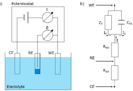
Voltammetry is usually performed in a three electrode configuration with a working electrode WE, a reference electrode RE and a counter electrode CE [2]. A schematic layout of an electrochemical cell in three electrode configuration and the corresponding equivalent circuit diagram are depicted in Fig. 2.1.
Figure 2.1: Schematic representation of an electrochemical cell. (a) Schematic layout of the three electrode configuration with working electrode (WE), counter electrode (CE) and reference electrode (RE). The potential (E) of the WE is measured and controlled versus the RE and the current (I) is measured versus CE with a potentiostat. (b) Equivalent circuit diagram of the electrochemical cell with the ohmic resistance of the solution Rsol, the capacity of the double layer at the electrolyte/electrode interface CDL and the Faraday impedance ZF representing material conversion. The corresponding current I can be divided in the charging current IC and the faradaic current IF. Adapted from [2].
As it can be seen in the schematic layout in Fig. 2.1, the applied potential E at the WE is measured versus RE and the corresponding current I is measured versus CE with a potentiostat. The measurement of E should preferably be carried out currentless versus RE as otherwise a proportion of the applied potential E is lost at the resistance of the solution Rsol. The effective applied potential Eeff at the WE is therefore described as:
Eeff = E − I ∙ Rsol (1)
Accordingly, electrochemical measurements should be performed in electrolytes with a low resistivity to reduce this parasitic effect (IR-drop) on the measurement results. From Fig. 2.1 b) it is evident that I is the
sum of two superimposed and inseparable current components, consisting of the charging current IC and the faradaic current IF.
I = IC+ IF (2)
Here, IC represents the charging of the double layer at the electrolyte/substrate at a potential step. The double layer can therefore be illustrated as a capacity element CDL in the equivalent circuit. Consequently, Ic is a time dependent function in dependence of CDL and Rsol at a potential step from E1 to E2.
IC=E2− E1
Rsol ∙ exp ( −t
Rsol∙ CDL) (3)
Contrary, IF is a result of the electrochemical conversion of the active species at the WE and starts at the characteristic half-wave potential of a reaction. This process is represented as the Faraday impedance ZF
in the equivalent circuit diagram [3]. Since the information of the reaction is only represented by IF,a large ratio IF/IC is favorable. This can be achieved by exploiting the time dependency of both current components by using pulsed techniques [4] or by utilizing microelectrodes (chapter 2.1.3.2). The process of the electrochemical conversion of the active species consists of three major steps and will representatively be explained for a reduction process. The overall process can be described schematically as:
Obulk→ Osurfacen∙e
−
↔ Rsuface→ Rbulk (4)
In the first step, the oxidized form of the active species O is transported towards the electrode surface at a diffusion-controlled rate DO. This mass transport can be described by the mass transport coefficient mT
in dependence of DO and the corresponding diffusion layer thickness δ:
mT=D0
δ (5)
In the second step, the electrons are transferred at the electrode surface, whereas the species O is reduced to its reduced form R. The reaction is kinetically controlled by the potential dependent reaction rate constant k. In the third step, the conversed species R is transported away from the electrode, controlled jointly by thermodynamics and diffusion DR of the reduced species. Each of the three steps contributes to IF by their partial currents of Idif, Ikin and It/d. Consequently, the measured faradaic current is expressed by the reciprocal formula [5]:
1 IF= 1
Idif+ 1 Ikin+ 1
It/d (6)
As it can be seen in (6), electrochemical conversion can be limited by one of the steps mentioned before.
Therefore, this process can basically be limited by mass transport or kinetics. Accordingly, an electrochemical conversion process can be categorized into reversible (fast kinetics) or irreversible (slow kinetics) processes by comparing mT with k [6]:
k ≫ mT (reversible) (7)
k ≪ mT (irreversible) (8)
For the following theoretical considerations, it is assumed that the electrode processes are reversible. As previously described, electrochemical conversion is dependent on mass transport towards the surface in this case. A more detailed description of the process of mass transfer will be given in the next chapter which is required to understand the behavior of macro- and microelectrodes.
2.1.2 Mass transfer towards the electrode surface
Mass transport is defined as the flux J of a mass or a species from one place to another place in the solution.
The flux is the result of a change of chemical potential or electrical potential between two locations or the movement of a volume element in this solution. It can be described by the Nernst-Planck equation in dependence of the aforementioned factors. For the one-dimensional stationary transport towards the electrode in x-direction J can be expressed in dependence of the active species i with diffusion coefficient Di, concentration ci, number of electrons transferred zi, electric potential Φ and velocity υ, the faraday constant F, universal gas constant R and temperature T as [7]:
Ji(x) = −Di∙∂ci(x)
∂x −zi∙ F
R ∙ T∙ Di∙ ci∙∂Φ(x)
∂x + ci∙ υ(x) (9)
One can see that J is the result of three independent terms. The first term of equation (9) describes the influence of diffusion on J. It is based on a concentration gradient arising from a difference in chemical potential. The second term of eq. 9 shows the impact of migration on the basis of the movement of charged particles in an electric field. The third term of eq. 9 characterizes the effect of natural or forced convection on J. Since these three terms are independent from each other, a simplification of eq. 9 is possible by suppression of one or two of the contributing terms. On this occasion, influence of migration can be eliminated by using a supporting electrolyte and the effect of convection can be suppressed by working in quiescent solution. Accordingly, mass transfer can be restricted to diffusive flux. In this case eq. 9 is simplified to the one-dimensional stationary Fick’s first law:
−Ji(x) = Di∙∂ci(x)
∂x (10)
Considering mass conservation without any chemical reactions in eq. 10, Fick’s second law can be obtained. This partial differential equation describes the diffusion dependent change of the concentration gradient with time.
∂ci(x, t)
∂t = Di∙ (∂2ci(x, t)
∂𝑥2 ) (11)
Or the general form of Fick’s second law for any geometry with the Laplacian operator ∇2:
∂ci
∂t = Di∙ ∇2 ci (12)
This Laplacian operator has to be modified dependent on electrode geometry. The corresponding Laplace operators are depicted in table 2.1.
Table 2.1: Laplacian operator for various electrode geometries. Adapted from [8].
Type Variables Laplacian operator ∇2 Example
Linear x ∂2
∂x2 Shielded disk electrode
Spherical r ∂2
∂r2+2 r∙ (∂
∂r) Hanging drop electrode
Cylindrical (axial) r ∂2
∂r2+1 r∙ (∂
∂r) Wire electrode
Disc r, z ∂2
∂r2+1 r∙ (∂
∂r) + ∂2
∂z2
Inlaid disk
ultramicroelectrode
Band x, z ∂2
∂x2+ ∂2
∂z2 Inlaid band electrode
By solving the general form of Fick’s second law, the time dependent current response at a fixed potential can be obtained in the case of diffusion limited processes. In the next chapter, a more detailed description of the current response of different planar electrodes will be presented.
2.1.3 Voltammetric behavior of macroelectrodes and microelectrodes
The solution of the general form of the partial equation of Fick’s second law is strongly dependent on the boundary conditions [8] and the Laplacian operator for the corresponding electrode geometry as it can be seen in table 2.1. Consequently, the current response of macro- and microelectrodes are not identical and have to be derived separately.
2.1.3.1 Macroelectrodes
The active area of a planar macroelectrode is large in comparison to the edges of aforementioned surface.
Accordingly, it can be assumed that the flux towards the electrode surface is controlled by linear diffusion since boundary effects at these edges are negligible. Due to this simplification, the one-dimensional form of Fick’s second law (eq. 11) can be used for calculation. This partial differential equation is solved by the Cottrell equation [6]:
I(t) =n ∙ F ∙ A ∙ √Di
√π ∙ t ∙ ci0 (13)
The Cottrell equation describes the time dependent decrease of current based on the consumption of initial concentration of the active species ci0 on an electrode area A and the amount of substance n. This equation can be used to predict the faradaic current response of a potential step experiment from E1 (no electrode reaction) to E2 (reaction at a diffusion-controlled rate) and is used to describe current transients in chronoamperometry (chapter 2.1.4.2). Since this equation is based on eq. 11, it is only valid for diffusion limited electrochemical conversion. The depletion of the active species at the electrode surface can be prevented by applying forced convection to the system for example by stirring or using a rotating disc electrode (RDE). Due to the enhancement of mass transfers (eq. 9), a time-independent stable diffusion layer is formed, and a constant faradaic current is obtained which does not follow the predicted Cottrellian behavior.
2.1.3.2 Microelectrodes
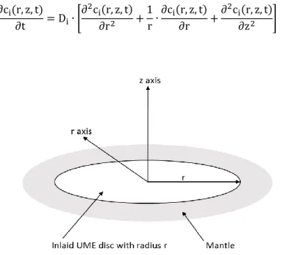
In the case of microelectrodes, boundary effects cannot be neglected since they provide a significant share to the mass transport. Accordingly, diffusion from the edges of the electrode surface has to be considered in eq. 12 by adapting the Laplacian operator according to table 2.1. Thus, Fick’s second law can be written in spherical coordinates for microelectrodes with an insulating mantle of infinite thickness as depicted in Fig. 2.2:
∂ci(r, z, t)
∂t = Di∙ [∂2ci(r, z, t)
∂r2 +1
r∙∂ci(r, z, t)
∂r +∂2ci(r, z, t)
∂z2 ] (14)
Figure 2.2: Schematic representation of an inlaid microelectrode with radius r and spherical coordinates.
Adapted from [5].
The time dependent current response for inlaid microelectrodes of a radius r with infinite mantle thickness is obtained by solving eq. 14 [5]. Since the solution is derived from Fick’s law, it is only valid for diffusion- controlled process:
I(t) =n ∙ F ∙ π ∙ r2∙ √Di
√π ∙ t ∙ ci0+ 4 ∙ n ∙ F ∙ Di∙ r ∙ ci0 (15)
As it can be seen, the current response of microelectrodes is described by two independent terms. The first term represents the time dependent current response based on linear diffusion. This term shows a Cottrellian behavior analogous to macroelectrodes (eq. 13). The second term is time independent due to the formation of a time independent spherical diffusion field at the edges of the electrode. Thus, the current response of this term represents a steady-state current behavior. Both terms are schematically depicted in Fig. 2.3.
Figure 2.3: Schematic representation of diffusion fields at a disc electrode with infinite mantle thickness.
(a) linear diffusion field and (b) spherical diffusion field of a microelectrode with radius r. Adapted from [5].
Since the Cotrellian term shows a quadratic dependency on electrode radius (I ∝ r2), its influence on the current response diminishes with decreasing electrode size in comparison to the second term (I ∝ r). Thus, for very small electrodes with r ≪ 50 µm, also referred to as ultramicroelectrodes (UME), the linear diffusion term approaches zero and the term for the spherical diffusion represents the significant fraction.
Consequently, the current response of microelectrodes in an insulating mantle of infinite thickness is described by a steady state current Iss, since the mass transport of the reactive species is controlled by a constant spherical diffusion layer formed around the microelectrode:
Iss= 4 ∙ n ∙ F ∙ Di∙ ci0∙ r (16)
For microelectrodes with finite mantle thickness, the flux from behind the electrode surface has to be considered as otherwise Iss will strongly differ from the value predicted by eq. 16. The mantle thickness rg
is usually normalized on the corresponding electrode radius r in order to be able to compare different microelectrodes sizes. Thus, the RG-value is calculated from the ratio between rg and r:
RG =rg
r (17)
Accordingly, the influence of the mantle thickness on Iss can be expressed by a β-function in dependence of RG with an error of less than 0.3% for RG > 1 [9].
Iss= 4 ∙ n ∙ F ∙ Di∙ ci0∙ r ∙ β(RG) (17)
With the β-function [9]:
β(RG) = 1 + 0.23
(RG3− 0.81)0.36 (18)
Besides their steady-state behavior, the usage of microelectrodes has further advantages in comparison to macroelectrodes. Since the electrode radius is proportional to the RC element (r ∝ RC, [5]), the utilization of smaller electrodes will minimize IC according to eq. 3. Consequently, a high IF/IC ratio can be obtained, which is advantageous for studying fast reactions. Moreover, the impact of IR-drops on Eeff is significantly reduced. Since the measured current for microelectrodes is usually in the range of nA to pA, the IR-drop is much lower according to eq. 1. Consequently, it can be assumed that Eeff ≈ E. For that reason, it is possible to work in high resistive solutions without the addition of a conductive salt. Furthermore, experimental studies can be carried out in two electrode configuration without the presence of a reference electrode when using microelectrodes. In the next chapter, common techniques in voltammetry are described. The impact of electrode sizes of macro- and microelectrodes in these methods are discussed.
2.1.4 Voltammetric techniques
There is a broad range of voltammetric techniques for quantitative and qualitative characterization in different application areas [7]. Since only cyclic voltammetry and chronoamperometry were used in this work, the focus is set on these techniques in the following chapter.
2.1.4.1 Cyclic voltammetry
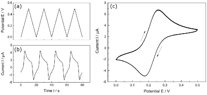
In cyclic voltammetry a saw tooth voltage profile is applied to the working electrode. The saw tooth voltage is thereby defined by a low and high vortex potential as initial/end potential. The selection of the vortex potentials is dependent on the conversion process of the redox active species. A cycle contains a linear increase of voltage from the initial potential to the end potential followed by linear decrease until the initial potential is reached by a predefined scan rate. The cycles are repeated as often as desired. During controlled potential cycling, the current at the WE is monitored. The logged current during measurement is plotted versus the applied potential, which is called a cyclic voltammogram. This diagram can be used to obtain electrochemical properties of a redox active species [6]. A representative measurement with ferrorecenemethanol (FcMeOH) as electroactive species is shown in Fig. 2.4.
Figure 2.4: Different data parts of a measurement in cyclic voltammetry. (a) Applied saw tooth potential E at the working electrode in dependence of time. (b) Measured current I due to potential change in dependence of time and (c) plot of cyclic voltammogramm I vs E resulting from the data of (a) and (b) with a Pt-macroelectrode (r = 1 mm) in a 1.5 mM FcMeOH and 0.2 M KNO3 mediator.
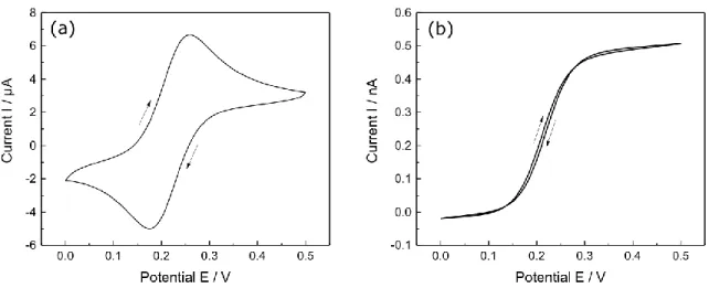
In cyclic voltammetry, different current responses are obtained based on electrode size. As shown in chapter 2.1.3, current response is dependent of the geometrical size of the active electrode area in the case of a diffusion limited reaction. Accordingly, current response for macroelectrodes and microelectrodes differs strongly as can be seen in Fig. 2.5 for a) a macroelectrode with r = 1 mm and b) an ultramicroelectrode with r = 12.5 µm (RG = 10).
Figure 2.5: Comparison of cyclic voltammograms at different electrodes. (a) Pt-macroelectrode (r = 1mm) and (b) Pt-microelectrode (r = 300 nm, RG = 10) in 1.5 mM FcMeOH and 0.2 M KNO3.
As can be seen, FcMeOH is oxidized at a heterogenous reaction rate at a certain starting potential. For the macroelectrode, a peak shaped response is obtained due to its Cottrellian behavior predicted by eq. 13.
The observed peak during potential increase is consequently the result of the current decay ( I ∝ 1 √t⁄ ) on the basis of the depletion of the surface concentration of FcMeOH. Furthermore, an offset between forward- and backward scan is observable. This effect can be attributed to the influence of Ic on the measured current due to the double layer charging during potential sweep as explained in chapter 2.1.1.
In contrast to the macroelectrode, a steady-state current response is obtained for microelectrodes. The plateau of the sigmoidal steady state voltammogram corresponds to the steady state current response of microelectrodes according to eq. 17. No offset between forward- and backward scan can be observed as the influence of Ic is strongly reduced for microelectrodes due to dependence of the RC element on tip size (chapter 2.1.3.2).
2.1.4.2 Chronoamperometry
In chronoamperometry, the potential of the working electrode is set to a fixed value and the current response is logged during measurement time. The obtained current responses are also referred to as current transients. This technique can be used to study nucleation processes, kinetics and diffusion processes [10]. Typical current transients for a diffusion limited reaction are plotted in Fig. 2.6.
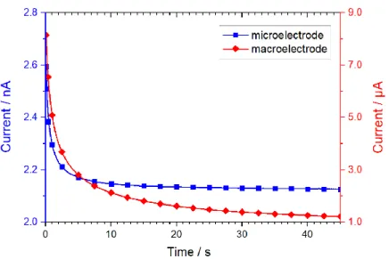
Figure 2.6: Current transients of a Pt-microelectrode (r = 6.25 µm, RG = 3) and a Pt-macroelectrode (r = 1 mm) at E = 0.5 V in 1.5 mM FcMeOH and 0.2 M KNO3.
As theoretically predicted in chapter 2.1.3, the current response is dependent on the size of the electrode.
For the macroelectrode, a decay of current is observed due to the Cottrellian behavior ( I ∝ 1 √t⁄ ) at the large active electrode according to eq. 13. The current is steadily decreasing due to the depletion of the active species at the electrode surface until the reaction is limited by diffusion of the species from the bulk solution. Contrary, a steady-state current response is obtained for microelectrodes due to the diffusion limited transport of the active species caused by the spherical diffusion field as predicted by eq. 17. Due to this steady state behavior as well as the fast response times according to chapter 2.3.1.2, it is possible to obtain electrochemical information in small spots of the solution with microelectrodes. These
advantageous properties are applied in the scanning electrochemical microscope (SECM). This measuring technique will be presented in the following chapter.
2.2 Scanning electrochemical microscopy
Scanning electrochemical microscopy (SECM) was developed and characterized by Bard and coworkers in 1989 [11]. SECM belongs to the class of scanning probe microcopy (SPM). In SPM a small probe is scanned across the surface whereby an image of the surface is obtained through the interaction of the probe with the surface. Using SECM, local information of the electrochemical behavior at the liquid/solid, liquid/gas and liquid/liquid interface can be obtained through the interaction of an ultramicroelectrode with the interface of interest. Consequently, insight into surface reactivity, chemical kinetics, and the local concentration of reactants can be obtained [11]. An introduction into this versatile electrochemical characterization tool will be presented in the following chapter.
2.2.1 Measurement setup of scanning electrochemical microscopy
A schematic illustration of the SECM setup is depicted in Fig. 2.7. The electrochemical measurement cell (SECM cell) contains the counter- and reference electrode, a mounting platform for a substrate, and the mediator. The design of the SECM cell is dependent of the substrate of interest. Measurements are usually performed in a four-electrode configuration with an UME as probe (WE1), a counter electrode (CE), a reference electrode (RE), and the substrate of interest as the second working electrode (WE2). The control of the electrode potentials and the data acquisition is achieved with a bipotentiostat [11].
Figure 2.7: (a) Schematic illustration of a scanning electrochemical microscope setup. (b) Geometry of a tip electrode with characterizing parameters: tip radius rtip, radius of insulating mantle rg and distance between tip and substrate d. Adapted from [12].
The position of the ultramicroelectrode is controlled with a stepper motor for large movements and a piezoelectric motor for very fine movements in three orthogonal directions. Thus, one can approach to the interaction range of the UME in z-direction and scan in the xy-plane for surface imaging. Data acquisition and probe movement is simultaneously controlled by software.
2.2.2 Electrochemical mediators
The choice of the mediator system is strongly dependent on the investigated substrate of interest (redox potential, pH condition, concentration). A mediator is basically characterized by a kinetically rapid one- electron reversible transfer reaction which is selective for the substrate of interest. Consequently, both mediator species, the reduced form R and an oxidized form O, have to be stable in solution. The solvent is usually water but other organic solvents like acetonitrile can also be used. In order to prevent the influence of dissolved oxygen on measurement results at the electrodes, the mediator solution is usually deaerated before measurement [11]. In this study, ferrocenemethanol (FcMeOH), hexamineruthenium (III) chloride
(Ru(NH3)6Cl3) and potassium octacyanotungstate (IV) dihydrate (K4W(CN)8∙2H2O) were used for surface characterization with SECM. Their half-cell reaction is depicted in table 2.2.
Table 2.2: Half-cell reaction of selected mediators. Adapted from [11].
Mediator Half cell reaction Standard potential (vs. NHE)
Octacyanotungstate (IV) dihydrate [W(CN)8]4−/3− 0.49 V Ferrocenemethanol (FcMeOH) [C11H12FeO]0/1+ 0.44 V Hexaamineruthenium (III) chloride [Ru(NH3)6]2+/3+ 0.05 V
2.2.3 Working modes in scanning electrochemical microscopy
In this chapter the basic working modes of SECM are covered. Since the presented studies are based on amperometric methods, a short overview of the major amperometric SECM techniques will be provided:
the feedback mode, the generation/collection modes and the competition mode. The choice of working mode is usually strongly dependent on the field of application. These working modes of SECM can be utilized for the characterization of surface reactivity of solid-state materials, electrocatalytic materials and enzyme activity in biochemistry [13].
2.2.3.1 Feedback mode
The feedback mode is the most commonly used working mode in SECM. This mode can be utilized in either a four-electrode or a three-electrode configuration in the case where biasing of the substrate at a fixed potential is not necessary. This technique allows for the precise positioning of the tip at a defined distance with respect to the substrate. The UME is set on a fixed potential E where the reactive species of the mediator is oxidized or reduced. As already shown in chapter 2.1.3.2, the electrochemical conversion at the UME tip is mass transport limited. Thus, the steady-state current in the bulk solution IT,∞ can be measured at the electrode tip according to eq. 17. Approaching the UME towards a substrate will result in a change of the measured tip current IT. In order to be able to compare the results of UME with different sizes, IT is normalized to IT,∞ and the tip-to-substrate distance d is normalized to rtip.
IL= IT
IT,∞ (19)
L = d
rtip (20)
In feedback mode, there are two limiting cases dependent on the surface conductivity. If the tip is approached towards an insulating surface (e.g. PTFE or glass) the diffusion of the reactive species towards the UME is blocked by the substrate, resulting in a decrease in measured current IT< IT,∞. The measured current reaches IT= 0 as the tip-to-substrate distance d reaches d = 0. This effect of current decrease is called a negative feedback. If the tip approaches a conductive surface (e.g. platinum or gold) the tip- generated species is regenerated at the substrate and diffuses back to the UME. As a result, the measured current will increase IT> IT,∞ due to an increase of the reactive species at the UME. The current can reach large values as the tip-to-substrate distance moves toward zero. The effect of current increase is called a positive feedback. Feedback is strongly dependent on rtip and and rg due to additional flux of mediator from the backside of the electrode. Accordingly, the influence of the RG-value on feedback has to be taken into account. Thus, the normalized tip current response for negative feedback ILins and positive feedback ILC can be described in dependence of L and RG for a diffusion controlled reaction according to [14,15].
Since these analytical equations can be correlated with experimental approach curves, UME characterization (rtip, rg) in a known mediator solution is possible.
ILins(L, RG) =
2.08
RG0.358∙ (L −0.145
RG ) + 1.585 2.08
RG0.358∙ (L + 0.0023 ∙ RG) + 1.57 +ln(RG)
L + 2
π ∙ RG∙ ln (1 +π ∙ RG 2 ∙ L)
(21)
ILC(L, RG) = α + π
4 ∙ β ∙ arctan(L)+ (1 − α − 1 2 ∙ β) ∙2
π∙ arctan(L) (22)
with α and β in dependence of RG:
α(RG) = ln(2) + ln(2) ∙ (1 −2
π∙ arccos ( 1
RG)) − ln(2) ∙ (1 − (2
π∙ arccos (1 RG))
2
) (23)
β(RG) = 1 + 0.639 ∙ (1 −2
π∙ arccos ( 1
RG)) − 0.186 ∙ (1 − (2
π∙ arccos ( 1 RG))
2
) (24)
For positive feedback a simplified approximation can be used as feedback is less influenced by mediator flux from the backside of the UME. The accuracy of ILC fits within 1% for 1.1 ≤ RG ≤ 10 [16].
ILC(L, RG) = A +B
L+ C ∙ exp (D
L) (25)
The empirical parameters A, B, C, and D in dependence of the RG-value are depicted in table 2.3.
Table 2.3: Parameter values for eq. 25, adapted from [16].
RG A B C D
1.1 0.5882629 0.6007009 0.3872741 -0.869822
1.5 0.6368360 0.6677381 0.3581836 -1.496865
2.0 0.6686604 0.6973984 0.3218171 -1.744691
5.1 0.72035 0.75128 0.26651 -1.62091
10 0.7449932 0.7582943 0.2353042 -1.683087
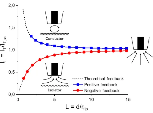
A schematic illustration of the feedback modes with the corresponding tip reactions is depicted in Fig. 2.8.
The approach curves were recorded in 1.5 mM FcMeOH and 0.2 M KNO3 with an UME of rtip = 13µm (RG > 10) towards insulating glass (red) and conductive platinum (blue) as substrate. The measured data are fitted with eq. 21 for negative feedback and eq. 25 for positive feedback.
Figure 2.8: Schematic representation of feedback. Steady state current far away from surface due to spherical diffusion at normalized distance L = 15. Positive feedback (blue) in close proximity to a conductive surface due to regeneration of tip-generated species. Negative feedback (red) near insulating surface due to blockage of diffusion. Experimental conditions: 1.5 mM FcMeOH/0.2 M KNO3 at Etip = 0.4 V with an UME of rtip = 13 µm (RG = 10). Adapted from [17].
2.2.3.2 Generation/Collection modes and Competition mode
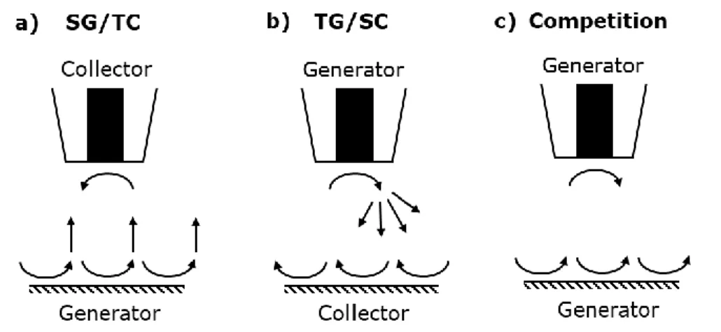
In contrast to feedback mode, four electrodes are required for this technique with the UME placed in interaction proximity of the substrate electrode. In the generation/collection modes the electroactive species is in situ generated at one of these electrodes and is collected at the other electrode after diffusion through the tip-substrate-gap. Since both, the substrate and the UME can act as the generator or the collector electrode, two generation/collection modes are existing. In the first case, the substrate is used as the generator electrode and the tip as the collector electrode (SG/TC mode) as illustrated in Fig. 2.9 a).
In this technique, the resolution as well as the screening area are limited due to the increasing background current over measurement time by the continuous formation of the active species at the substrate electrode. In the second case the tip is used to generate the active species and the substrate electrode for
collection of this species (TG/SC mode) as depicted in Fig. 2.9 b). The advantage of TG/SC is its small background signal due to the local generation of the active species at the UME tip. Therefore, TG/SC mode is only suited for small substrates since its sensitivity decreases with substrate electrode area [18].
Figure 2.9: Schematic representation of different generation modes. a) Substrate generation/tip collection mode (SG/TC mode), b) tip generation/substrate collection mode (TG/SC mode) and c) both electrodes as generation electrodes (Competition mode).
The collection efficiency η for the generation/collection modes can be quantified by calculating the current ratio between the substrate current IS and the tip current IT.
η =IS
IT (26)
The efficiency is strongly dependent on the tip-to-substrate distance and is usually approximately η ≈ 1 for TG/SC mode and η ≪ 1 for SG/TC mode. Both modes are applicable methods for studying electrocatalysts, for example in the field of hydrogen evolution reaction (HER) or in oxygen evolution reaction processes [19]. In contrast to the generation/collection modes, substrate and tip electrode are both used as generator electrodes in the competition mode as it can be seen in Fig 2.9 c). Since both electrodes are competing for the same species, the decrease in measured tip current represents the local catalytic activity of the substrate surface. Thus, the sensitivity is not affected by the substrate area in
competition mode in contrast to the TG/SC mode. As a consequence, the resolution can be further increased in competition mode by the usage of smaller UMEs [20].
2.2.4 Imaging process
Imaging describes the process in which the surface is scanned by the tip in the XY plane. Thus, local information about the electrochemical activity and topography of the substrate can be obtained due to surface interaction of the tip in the scanning process. The resolution is dependent on rtip, RG-value, scan speed, and the tip-to-substrate distance. Accordingly, the tip must be brought into working distance before the imaging process [17]. This can be achieved by approaching the UME in feedback mode in a defined mediator solution as described in chapter 2.2.3.1. Two common imaging modes are applicable as it can be seen in Fig 2.10.
Figure 2.10: Schematic illustration of imaging modes. (a) Constant height and (b) constant distance.
Adapted from [21].
In constant height mode the UME is scanned in XY plane at a fixed distance L between tip and substrate.
This mode is commonly used for substrates with smooth surfaces and can be utilized in feedback, SG/TC, TG/SC, and competition mode. When scanning in fixed L, problems can arise with surface topography. If the roughness is too large, it is possible that the tip crashes into the substrate at topographic hills or that the surface interaction is lost in topographic valleys (see red crosses in Fig. 2.10). In constant distance mode, the gap between tip and substrate is kept at a constant level by adjusting the z-position of the tip in dependence of the measured tip signal [22]. This mode is limited by the response speed of the distance
control mechanism at strong changes in topography. Since the measured signal in SECM is strongly dependent on the distance between tip and substrate in both modes, local information on topography and electrochemical activity cannot be obtained independently in the imaging process. Accordingly, surface topography can only be obtained in pure negative or pure positive feedback from homogenous materials.
2.3 Electrochemical deposition of copper
2.3.1 Electroplating of copper in semiconductor industry
Electroplating of copper (Cu) was introduced in the semiconductor industry by IBM in 1997 due to good electrical and thermal conductivity as well as the higher resistance to electromigration of copper in comparison to aluminum (Al) [23]. Electrochemical Cu deposition is usually carried out from an acidic Cu electrolyte on a Cu seedlayer (PVD) deposited prior to electroplating.
2.3.1.1 Copper electrolyte
A conventional acidic bath contains inorganic and organic compounds for void free filling of structured surfaces. The inorganic compounds consist of copper(II) sulfate (CuSO4) as Cu source with c(Cu2+) > 10 g/l, sulfuric acid (H2SO4) for conductivity increment of the solution and to prevent the precipitation of the Cu salt. Further, small amounts of hydrochloric acid (HCl) (c(Cl-) < 100 ppm) are needed to ensure the surface interaction of the organic compounds during the electrochemical deposition process. The organic bath compounds consist usually of three additives which are selectively influencing Cu deposition. The first organic component, the accelerator, is locally enhancing Cu electrodeposition due to its capability to reduce surface potential and to facilitate ion transfer to the surface. Molecules with a thiol-group, for example sulfopropyl-disulfide (SPS) can be used as accelerator. The second organic component, the suppressor, inhibits the Cu deposition locally by the formation of a stable complex with Cu(I) ions and Cl ions at the Cu surface such as polyethylenglycol (PEG). The third organic component, the leveler, facilitates selective filling of trenches and vias due to the accumulation of this additive on edges and corners with high electric field strength. Thus, the local difference between recessed areas and bumps can be balanced.
Usually coloring agents are used as leveler additives, for example Janus Green B (JGB) or polyvinylpyrrolidone (PVP) [24]. Via a suitable concentration ratio of these three additives, it is possible to achieve homogeneous galvanic copper deposition on wafer level scale.
2.3.1.2 Electroplating tool
Electrodeposition from this Cu electrolyte is performed in a two-electrode setup with the structured wafer as cathode and solid copper as anode material. A schematic illustration of a commercial plating tool is depicted in Fig. 2.11.
Figure 2.11: Schematic illustration of a commercial plating tool in semiconductor industry. The electrolyte tank is separated in two compartments by a semipermeable membrane. The electrolytes in both chambers are continuously circulated. The anode chamber contains the anode and the anolyte (CuSO4, H2SO4, HCl).
The cathode chamber is constructed as an overflow tank and includes the rotatable mounting platform for the wafer as well as the catholyte (CuSO4, H2SO4, HCl, leveler L, accelerator A, suppressor S).
In order to be able to act as the cathode, the Cu seedlayer on the wafer is electrically contacted and sealed from the edges in a mounting platform prior to immersion in the overflow tank. To stabilize the Cu bath, the interaction of the inorganic compounds with the Cu anode is prevented (US6126798A, [25]). Therefore, the electrolyte tank is divided into two separate individually circulated compartments by a semipermeable membrane. Thus, the cathode chamber contains the catholyte with the inorganic and organic compounds of the electrolyte and the anode chamber includes the anolyte with only the inorganic compounds. The
concentration of Cu in the catholyte is maintained by the diffusion of Cu ions from the anolyte to the catholyte due to the concentration gradient during deposition according to eq. 27 and eq. 28. In order to simulate this wafer scaled deposition process on the laboratory level, a dedicated miniaturized plating cell is utilized for the experimental studies as described in chapter 4.1.
Cathode Cu2++ 2e−→ Cu (27)
Anode Cu → Cu2++ 2e− (28)
2.3.1.3 Deposition rate of galvanic copper
The galvanic deposition process is carried out in direct current or in a pulsed technique at a predefined deposition rate [24]. This deposition rate is based on Faraday’s laws of electrolysis which describe the relationship between flowed charge Q, the valency number of ions z, the Faraday constant F and the amount of substance n. Here, n can be expressed as a function of mass m and molar mass M as depicted in eq. 29.
Q = n ∙ z ∙ F =m
M∙ z ∙ F (29)
Utilizing the relationship between Q, the applied current I and the deposition time t in eq. 30, Faraday’s law can be expressed as a function of flowed current.
Q = I ∙ t (30)
Furthermore, implementing the correlation between m, density ρD, and volume V, which is the product of deposited area ADep and thickness d as described by eq. 31, the deposition rate d/t can be expressed as a function of the above-mentioned variables by assuming 100% current efficiency (32):
m = ρ ∙ V = ρ ∙ ADep∙ d (31)
d
t = M
ρ ∙ z ∙ F∙ I
ADep= const ∙ I
ADep= const ∙ j (32)
As can be seen in eq. 32, d/t is only dependent on the ratio of I and ADep and therefore on current density j.
Consequently, the deposition rate can be adjusted by changing the applied current density in the galvanic Cu deposition process.
2.3.2 Barrier films for copper
Since Al was replaced by Cu metallization as interconnect material [23], barrier films (also referred as liner materials) became mandatory to prevent the diffusion of Cu (DCu= 3 ∙ 104m2⁄s, [26]) into the surrounding dielectrics and Si. It is known that Cu has a strong impact on the function of active elements due to their capability to form silicides like Cu3Si or deep trap states on the basis of agglomeration. For this reason, the complete encapsulation of Cu structures in a barrier material is necessary. Moreover, these barrier layers have to fulfill several further requirements such as sufficient mechanical stability, good adhesion between dielectric and interconnect, immiscibility with Cu, and the capability to act as etch-stop on top of interconnects. There are a variety of different deposition techniques to achieve the full embedment of Cu in liner materials. Commonly used techniques are physical vapor deposition (PVD) for bottom and side walls, atomic layer deposition (ALD) for conformal deposition in high aspect ratios, chemical vapor deposition (CVD) for contact level, and plasma enhanced chemical vapor deposition (PECVD) for coverage of the top of the interconnects [26]. A schematic cross section of a Cu interconnect with the corresponding barriers films is depicted in Fig. 2.12.