Magnetoconductance correction in zinc-blende semiconductor nanowires with spin-orbit coupling
Michael Kammermeier,*Paul Wenk, and John Schliemann
Institute for Theoretical Physics, University of Regensburg, 93040 Regensburg, Germany Sebastian Heedt,†Thomas Gerster,‡and Thomas Schäpers
Peter Grünberg Institute (PGI-9) and JARA-Fundamentals of Future Information Technology, Forschungszentrum Jülich, 52425 Jülich, Germany
(Received 8 September 2017; revised manuscript received 1 November 2017; published 6 December 2017) We study the effects of spin-orbit coupling on the magnetoconductivity in diffusive cylindrical semiconductor nanowires. Following up on our former study on tubular semiconductor nanowires, we focus in this paper on nanowire systems where no surface accumulation layer is formed but instead the electron wave function extends over the entire cross section. We take into account the Dresselhaus spin-orbit coupling resulting from a zinc-blende lattice and the Rashba spin-orbit coupling, which is controlled by a lateral gate electrode. The spin relaxation rate due to Dresselhaus spin-orbit coupling is found to depend neither on the spin density component nor on the wire growth direction and is unaffected by the radial boundary. In contrast, the Rashba spin relaxation rate is strongly reduced for a wire radius that is smaller than the spin precession length. The derived model is fitted to the data of magnetoconductance measurements of a heavily doped back-gated InAs nanowire and transport parameters are extracted. At last, we compare our results to previous theoretical and experimental studies and discuss the occurring discrepancies.
DOI:10.1103/PhysRevB.96.235302 I. INTRODUCTION
Despite the intensive research over the past decade, semiconductor nanowires continue to be one of the most active research areas within the nanoscience community [1]. The significant attention is due to the vast scope of technical applications [2–6] as well as the capability to conduct fundamental studies, such as the search for Majorana bound states [7,8]. Another broad field of interest concerns the utilization for spintronic devices, which exploit the spin degree of freedom of the charge carriers. The underlying effect, which allows to manipulate the spin, is the spin-orbit coupling (SOC). To understand the behavior of the spin and control it efficiently, a detailed knowledge about system parameters is essential. One basic and convenient tool to gather the desired information are weak-field magnetoconductance measurements. In disordered systems, the conductivity is either enhanced or reduced due to quantum interference, which is denoted as weak antilocalization (WAL) or weak localization (WL), respectively. By fitting the experimental data with an appropriate theoretical model, it is possible to extract SOC strengths as well as dephasing, scattering, and, most prominently, spin relaxation rates [9–18]. Notably, a crossover from WAL to WL can even indicate spin-preserving symmetries [19–21].
The huge degree of freedom in the device preparation process allows to manipulate many of the nanowire properties over a wide range. More precisely, one is able to effectively control the size, morphology, potential landscape, carrier, and
*michael1.kammermeier@ur.de
†Present address: QuTech, Delft University of Technology, 2628 CJ Delft, The Netherlands.
‡Present address: Physikalisch-Technische Bundesanstalt (PTB), Bundesallee 100, 38116 Braunschweig, Germany.
impurity concentration, or even crystal structure [12,22–31].
Since typically both the SOC and the WAL/WL correction strongly depend on these characteristics, the great diversity makes it difficult to build up a general theoretical description.
In fact, a variety of theoretical models are needed to appro- priately characterize the differing nanowires. The WAL/WL effect in the diffusive regime was analyzed by Kettemann [32]
and Wenk [33,34] for planar quantum wires with a zinc-blende lattice. In our preceding article [14], we developed a model for diffusive zinc-blende nanowires where the transport is governed by surface states, which occurs in materials with Fermi level surface pinning [12,25,30,35,36] or core/shell nanowires [26].
In this paper, we discuss the situation where the confining potential is flat over the total cross section. The motion of the electrons is considered diffusive in three dimensions (3D) and the nanowire radiusRmuch larger than the mean-free pathle. We take into account the Dresselhaus SOC resulting from the zinc-blende crystal structure and the Rashba SOC, which is controlled by a lateral gate electrode. Using this, we compute analytically the WAL/WL correction as a function of the nanowire radius. The spin relaxation rate due to Dresselhaus SOC is found to be independent of the orientation of the spin density, the wire growth direction, and the wire radius. In contrast, the Rashba spin relaxation rate is strongly reduced for a wire radius that is smaller than the spin precession lengthLso. If Rashba SOC is present, the long-lived spin densities have a helical structure and, elsewise, are homogeneous in real space.
At last, we fit the derived formulas to experimental data of a heavily doped InAs semiconductor nanowire, which shows a gate-induced crossover from WL to WAL. Thereby, we extract spin relaxation and dephasing rates as well as SOC strengths.
To complete our study, we compare our results to the frequently used one-dimensional (1D) magnetoconductance formula of Kurdaket al.[37] and discuss the discrepancies in the resulting fits and the gained transport parameters [9–11,13,15–18].
II. HAMILTONIAN FOR BULK ELECTRONS The HamiltonianHwhich describes bulk electrons in the lowest conduction band of a zinc-blende type semiconductor with SOC reads as
H= h¯2k2
2m +HR+HD. (1)
The terms
HR=γR[(kyEz−kzEy)σx+c.p.], (2) HD=γD
kx
ky2−kz2
σx+c.p.
, (3)
with cyclic permutations (c.p.) of preceding indices, denote the Rashba (R) and Dresselhaus (D) SOC contributions with the material-specific parametersγi, the electric field components Ei, the Pauli matricesσi, and the effective electron mass m [38–40]. In this notation, the underlying basis vectors{ˆx,ˆy,ˆz}
point along the crystal axes [100], [010], and [001]. We begin with the assumption that the electrons in the wire experience a nearly homogeneous electric field perpendicular to the wire axis. In Sec.IVwe will see that the choice of the wire axis and the perpendicular electric field is arbitrary as the Rashba and Dresselhaus SOC do not mix with each other in the Cooperon and the effect of the Dresselhaus SOC is independent of the crystal direction. Thus, without loss of generality, we define the wire axis to be oriented alongˆzand the electric field asE=Eˆy.
III. QUANTUM CORRECTION TO THE CONDUCTIVITY Within diagrammatic perturbation theory taking into ac- count the quantum interference between self-crossing paths in a disordered conductor gives rise to the first-order correction to the Drude conductivityσ. The following preconditions on the impurity potential Vimp(r) are assumed: (i) We consider a standard white-noise model for the impurity potential, meaning that it vanishes on average and is uncorrelated, i.e., Vimp(r) =0 andVimp(r)Vimp(r) ∝δ(r−r), respectively.
(ii) The disorder is weak, i.e., ¯h/(Fτe)1, whereF is the Fermi energy and τe is the mean elastic isotropic scattering time. Moreover, the motion of the electrons is considered diffusive in all three spatial directions. By averaging over all impurities and summing up all maximally crossed ladder diagrams, we find the quantum correction to the longitudinal static conductivity [41] to first order in ¯h/(Fτe) given by the real part of the Kubo-Greenwood formula
σ = 2e2 h
¯ hDe
V Re
⎛
⎝
Q,s,ms
χss,ms|C(Q)|ˆ s,ms
⎞
⎠. (4) Here,V is the volume of the nanowire,De the 3D diffusion constant, i.e.,De=v2Fτe/3, with the Fermi velocityvF, ˆCthe Cooperon propagator, and Q=k+k the sum of the wave vector of an electron with spinσ and the wave vector of an electron with spinσ. The factorχs is defined asχ0=1 and χ1= −1. Furthermore, the states|s,msrepresent the singlet- triplet basis of the system with two electrons, that is, s∈ {0,1} is the total spin quantum number and ms ∈ {0,±1}
the corresponding magnetic quantum number. We emphasize, that there exists a unitary transformation which associates the triplet basis states with the components of the spin density as
shown in Ref. [33] and defined in Appendix A. Below, we follow the approach in Refs. [14,32–34,42] to compute the quantum correction to the conductivity.
IV. 3D COOPERON
As SOC constitutes a small perturbation to the kinetic part in the HamiltonianHand the main contribution to the Cooperon results from terms nearQ=0, the Cooperon propagator ˆCcan be approximated by
C(Q)ˆ = τe
¯ h
1−
d 4π
1 1−iτe(Q)/ˆ h¯
−1
, (5) where ˆ(Q)= H(Q−kF,σ)−H(kF,σ) and the integral is performed over all angles of the Fermi wave vector kF. In 3D, the Fermi contour is nearly spherical and the integral is continuous. SinceFτe/h¯1, we may further ap- proximate ˆ(Q)≈ −vF( ¯hQ+2m(ˆaR+ˆaD)S) with the total electron spin vectorSin the singlet-triplet basis as defined in AppendixB. The matrixˆaR(ˆaD) contains the contributions due to Rashba (Dresselhaus) SOC, i.e.,
ˆaR= αR
¯ h
⎛
⎝ 0 0 1
0 0 0
−1 0 0
⎞
⎠ (6)
and
ˆaD= γD
¯ h
⎛
⎜⎝
k2y−k2z 0 0 0 kz2−k2x 0 0 0 kx2−ky2
⎞
⎟⎠, (7)
whereαR=γRE. For convenience and in analogy to previous publications [14,33,34,42], we define the Cooperon Hamilto- nian ˆHc=( ¯hDeC)ˆ−1. An additional Taylor expansion of the integrand in Eq. (5) to second order in [ ¯hQ+2m(ˆaR+ˆaD)S]
yields
Hˆc/Q2so =(Q+2eAs/h)¯ 2+λDS2/2 (8) in terms of the dimensionless momenta Qi =Qi/Qso with Qso=2mαR/¯h2=2π/LsowhereLsois the Rashba spin pre- cession length. Similar to the 2D and quasi-1D cases [14,32], the effect of Rashba SOC becomes manifest in an effective vec- tor potentialAs=QsoAs where As =h/(2e)(S¯ z,0,−Sx) and therefore couples to the Cooperon momentum. In contrast, the Dresselhaus SOC leads to a term∝λD=82/35, where =k2FγD/αR, which does not couple to the wave vectorQ and is diagonal in the triplet sector. Thus, it gives rise to a spin relaxation rate which is identical for all components of the spin density. We stress that unlike in tubular wires [14], the Dresselhaus contribution does not mix with the Rashba contribution and does not depend on the growth direction of the wire due to the averaging over the Fermi contour. Hence, the result applies to any zinc-blende nanowire irrespective of the growth direction and for an arbitrarily oriented electric field perpendicular to the wire axis.
V. EFFECTS OF A RADIAL BOUNDARY
The finite-size geometry of the nanowire requires a bound- ary condition for the Cooperon [32,43–45]. For an insulating
surface and spin-conserving boundary the condition reads as ˆn·(∇+2ieAs/h) ˆ¯ C|S =0, (9) whereˆndenotes the normal vector of the surfaceS. This condi- tion accounts for a specular boundary, which is plausible since the nanowires possess only a small degree of surface roughness [46]. Aside from that, in the transverse diffusive regime the ramifications of a diffusive boundary are insignificant [47].
The equation above can be simplified to a Neumann boundary condition, i.e., ˆn·(∇Cˆ)|S =0, by applying a non-Abelian gauge transformation. Thereby, the Cooperon (and with it the Cooperon Hamiltonian) is transformed as ˆC→Cˆ=UACˆUA† with the unitary transformation operator UA=exp[i2e(ˆn· As)(ˆn·r)/h]. In this case, the lowest Cooperon mode¯ |0 corresponds to a solution which has a vanishing wave vector perpendicular to the surface, i.e., ˆn·Q=0, and is thus constant in coordinate space alongˆn[45].
For a cylindrical nanowire, we identify ˆn=ρˆ and the surfaceS is defined by the constraintρ=R whereR is the radius of the wire and we introduced the standard cylindrical coordinates (ρ,φ,z) with the corresponding basis vectors {ρˆ,φˆ,ˆz}. Accordingly, the unitary transformation operator reads asUA=exp[i2e(ρˆ·As)ρ/h]¯ =exp[iQsoxSz] and the boundary condition becomes ρˆ·(∇Cˆ)|ρ=R =0. Using this, we obtain the transformed Cooperon Hamiltonian ˆHcas
Hˆc/Q2so =Q2−2Qz[cos(Qsox)Sx−sin(Qsox)Sy] +cos2(Qsox)S2x+sin2(Qsox)Sy2
−sin(Qsox) cos(Qsox){Sx,Sy} +λDS2/2. (10) The Dresselhaus contribution remains unchanged since [Si,S2]=0. A suitable and generic basis which satisfies the Neumann boundary condition is
r|n,l,Qz =Jl(n)(ρ)eilφeiQzz/Nnl, (11) with the angular momentum quantum numberl∈Z, the quasi- continuous plane-wave numberQzalong the wire axis, and an appropriate normalization constantNnl. The radial dependence is given by the Bessel function of the first kind Jl(n) which has itsnth extremum (n∈N+) at the nanowire surface, i.e., ρ=R. Additionally, we defineJl(0)=δl,0which corresponds to a constant solution in the x-y plane and constitutes the lowest mode ofHc, thus,|0 ≡ |n=0,l=0,Qz.
VI. ZERO-MODE APPROXIMATION
In order to obtain an analytical result, the transformed Cooperon ˆCcan be evaluated only for the lowest mode |0. This approach is often termed zero-mode or zero-dimensional approximation [32,44,45]. Using this approximation, the eigenvalues of0|Hc|0read as
E(0)S /Q2so =Q2z, (12) ET ,0(0)/Q2so =Q2z+λD+aso/2, (13) ET ,(0)±/Q2so =Q2z+λD+1−aso/4
±1 4
aso2 +64(1−bso)2Q2z, (14)
FIG. 1. Comparison of the zero-mode approximation (yellow) [Eqs. (12)–(14)] with the exact diagonalization of ˆHc(blue) truncated to nmax=4 and |lmax| =4 forλD=0.1 and (a) QsoR=0.3 and (b)QsoR=1.5.
where we introduced aso=1−2J1(2QsoR)/(2QsoR) and bso=1−2J1(QsoR)/(QsoR) with the Bessel function of the first kindJ1. We stress that the spectrum is identical for a planar wire [32] ifλD=0 and the function 2J1(x)/x is replaced by sin(x)/x. In Fig.1we compare the zero-mode approximation with exact diagonalization for different values ofQsoR. As the zero-mode approximation provides reliable results for small values ofQsoR <1 [33], we can write the triplet spectrum as ET ,0(0)/Q2so =Q2z+0, (15) ET ,(0)±/Q2so =(Q0± |Qz|)2+1, (16) where0=λD+aso/2,1=λD+2bso−aso/4, andQ0 = 1−bso. This has the following advantages. First, we capture the most important features of the spectrum, that is, the minima of the triplet modes j, which are direct measures of the
spin relaxation rate. ForET ,(0)±the minimum is shifted to finite momentaQz= ±Q0 and the corresponding long-lived spin densities are, therefore, of helical structure. Second, the simple form of the spectrum allows to derive a closed-form expression for the magnetoconductance correction later on.
VII. SPIN RELAXATION IN NARROW WIRES In general, four mechanisms have been found to be relevant for the relaxation of the spin of conduction electrons in metals and semiconductors: the D’yakonov-Perel’, Elliott-Yafet, Bir- Aronov-Pikus, and hyperfine-interaction mechanism [39]. In our approach, we account only for the D’yakonov-Perel’
mechanism [48], which has shown to be a very efficient source of spin relaxation.
The D’yakonov-Perel’ spin relaxation rate is related to the gaps in the Cooperon spectrum via the relation (1/τs)j = DeET ,j. This is a direct consequence of the fact that there exists a unitary transformation (AppendixA) which links the Cooperon with the spin diffusion equation [33]. Hence, in general, (1/τs)j depends on the Cooperon wave vectorQas well as on the orientation of the given spin state which is subject to a random walk. For a spatially homogeneous spin densityQ=0, the result is equivalent to the eigenvalues of the D’yakonov-Perel’ spin relaxation tensor [39].
In the bulk, the 3D Cooperon can be simply evaluated in the basis of plane waves. ForQ=0 the Cooperon Hamiltonian (5) is diagonal in the basis of spin density components (Ap- pendixA), leading to the 3D spin relaxation rates (1/τs)ii = DeQ2so(λD+1+δi,y) wherei∈ {x,y,z}. Unlike Rashba SOC, the Dresselhaus SOC affects the spin relaxation of all spin density components in the same way.
In presence of a radial boundary condition, the corre- sponding gauge transformation leads to a position dependence of the eigenstates of the Cooperon Hamiltonian Hc. In Appendix C, the Cooperon Hamiltonian Hc in zero-mode approximation is given in the basis of spin density com- ponents. For Qz=0, the sz component is fully decoupled and independent of the location on the wire cross section.
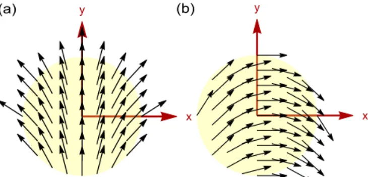
As a consequence, a spin density which is homogeneously polarized along the wire axis is an eigenstate of the Cooperon Hamiltonian and decays according to the spin relaxation rate (1/τs)zz=DeQ2so(λD+1). Remarkably, this rate is in- dependent of the wire radius to all orders in QsoR within the zero-mode approximation. In fact, it is identical to the 3D spin relaxation rate. The remaining two (unnormalized) eigenstatesa,j, wherea,−=(tan(Qsox),1,0) anda,+= (1,−tan(Qsox),0), with the according spin relaxation rates (1/τs),j =DeQ2so(δj,−±aso/2+λD) lie in the plane of the cross section and depend on the position as depicted in Fig.2.
In analogy to numerous previous works [32,49–52], we define hereafter the spin relaxation rate of the system 1/τs
as the minimal rate forQz=0, which is 1/τs≡(1/τs),+= DeQ2so(aso/2+λD). In the limit ofQsoR1, corresponding to a radiusR much smaller than the Rashba spin precession lengthLso, we replaceaso→4bso →(QsoR)2/2, which gives
1 τs
=kF2α2Rτe
3 ¯h2 (QsoR)2+32kF6γD2τe
105 ¯h2 (17)
FIG. 2. Eigenstates (a)a,−/a,−and (b)a,+/a,+of the Cooperon Hamiltonian in zero-mode approximation (AppendixC) forQsoR=1. Both states lie in the plane of the nanowire cross section (yellow).
to second order in QsoR. Noting further that since Qsox QsoR 1, the respective eigenstate is a,+≈(1,0,0). In accordance with Ref. [32], the first term in Eq. (17) is strongly suppressed in wires with small radii. However, compared to Ref. [32] the first term is a factor 2 smaller if we associated R=W/2, where W is the width of the planar quantum wire. The Dresselhaus-dependent spin relaxation rate was also obtained in Ref. [53]. Notably, as seen from Eq. (16), the global minimum of the spectrum is found at finite wave vectorsQz= ±Q0 and given by 1 which is for small λD approximately half as large as0. This outlines the superior spin lifetime of helical spin densities, which was observed earlier in planar and tubular two-dimensional electron gases (2DEGs) [14,19,32].
VIII. GENERAL REMARKS
First, we would like to point out some general observations on the structure of the Cooperon Hamiltonian ˆHc [Eq. (8)]
with respect to the presence of a generic SOC contribution.
Linear and cubic SOC terms can be always expanded in terms of first- and third-degree spherical harmonics in the wave vectork. Only the first-degree spherical harmonic terms can be rewritten in the form of an effective vector potentialAs
in the Cooperon Hamiltonian. In the present case, e.g., the bulk Dresselhaus SOC consists only of third-degree spherical harmonic terms, which leads to the structure of Eq. (8). Owing to the effective vector potential, the minimum of ˆHcis shifted to finite Cooperon wave vectorsQmin.
This has important consequences when the Cooperon Hamiltonian is subject to an insulating spin-conserving bound- ary condition as a result of a finite-size geometry (cf. Sec.V).
In particular, the component of the effective vector fieldAs
which is perpendicular to the surface is removed by a gauge transformationUA. Thereby, the component of the minimum in direction of the boundary, i.e., ˆn·Qmin, is shifted to zero wave vector after the transformation, i.e.,UA(ˆn·Qmin)UA† = 0. Since the lowest Cooperon mode typically corresponds to a constant solution in coordinate space, 0|ˆn·Q|0 =0 holds true and the remaining gauge-transformed (and therefore position-dependent) terms are averaged along the confined directions. This generates a suppression of the spin relaxation rate in small wires (in zero-mode approximation), which
is denoted as motional narrowing as it is observed in the cylindrical wire in this work and also earlier in planar quantum wires [32–34]. In both cases, the spin relaxation due to first-degree spherical harmonic SOC terms is strongly suppressed for wires of widths much smaller than the spin precession length. A finite relaxation remains, however, due to the third-degree spherical harmonic contributions.
Hence, the effect of motional narrowing is expected to be maximal if the entire effective vector potentialAsis removed.
Here, the cylindrical nanowire can take an outstanding role as it has a boundary in radial direction for the Cooperon, in contrast to the planar quantum wire that has a boundary along one Cartesian coordinate only.
IX. MAGNETIC DEPHASING
For experimental probing, we need to take into account the phase breaking due to a magnetic field. Disregarding SOC, the Cooperon propagator ˆCin real space is defined through the diffusion equation [43,45]
[ ¯hDe(i∇−2eA/h)¯ 2+h/τ¯ φ] ˆC(r−r)=δ(r−r), (18) with the magnetic vector potentialAand the dephasing rate τφ. This equation has the general solution
Cˆ(r−r)=
n
∗n(r)n(r)/( ¯hDeEn+h/τ¯ φ), (19) where n solve the eigenvalue equation (i∇− 2eA/h)¯ 2n(r)=Enn(r) with the according eigenenergy En. If we choose a gauge such that the vector potential has no component perpendicular to the surface, i.e., ˆn·A=0, the vector potential does not affect the boundary condition (9). For small magnetic fields, we can treat the terms
∝A in the eigenvalue equation perturbatively in zero-mode approximation. Assuming a Coulomb gauge with0|A|0 =0, we obtain in lowest order the magnetic phase shift rate as
1/τB =De(2e/h)¯ 20|A2|0, (20) where the expectation value is equivalent to the average taken over the sample geometry. The same expression is found by Beenakkeret al.in Ref. [54].
If a cylindrical nanowire with the surface vector ˆn=ρˆ is placed in a magnetic field perpendicular (B⊥=Bˆy) or parallel (B=Bˆz) to the growth axis ˆz, the corresponding vector potentials that fulfill the above-mentioned criteria areA⊥= Byˆz and A =B(xˆy−yˆx)/2. Consequently, the respective magnetic phase shift rates become 1/τB,⊥=De(eBR/h)¯ 2 and 1/τB,=1/(2τB,⊥). Note that here the magnetic field is assumed to be small enough such that the magnetic length [43]
lB =√
¯
h/(2e|B|) exceeds the wire width.
X. MAGNETOCONDUCTANCE CORRECTION For cylindrical semiconductor nanowires of lengthLand radius R, the macroscopic magnetoconductance correction Gfollows the relationG=(π R2/L)σ. More explicitly, using the groundwork of the preceding paragraphs we find in
zero-mode approximation σ(0)(B)= 2e2
h 1 R2π2Qso
√ce 0
dQz
1
E(0)S /Q2so+cφ+cB
−
j∈{0,±}
1
ET ,j(0)/Q2so+cφ+cB
, (21)
withci =1/(DeQ2soτi) wherei∈ {e,φ,B}. The exact result for the magnetoconductance correction is obtained by analogously summing over all eigenmodes of the Cooperon Hamiltonian, that is,G=
nG(n). We stress that the upper cutoff√ ce
due to the scattering rateτe, to remove the divergence, is strictly speaking only required in 2D. Thus, neglecting the upper limit
√ce and using the simplified triplet spectrum forQsoR <1 [Eqs. (15) and (16)], we obtain the closed-form expression
σ(0)(B)= 2e2 h
1 2π QsoR2
1
√cφ+cB − 2 1+cφ+cB
− 1
0+cφ+cB
, (22)
which resembles the result in Ref. [32]. In the following, we apply the developed model to fit magnetoconductance measurements.
XI. EXPERIMENTAL DATA FITTING
Exemplarily, we present the fitting results for a heavily n-doped InAs nanowire. As previously shown [14,30,36], the electrons in undoped InAs nanowires are confined to a narrow layer beneath the surface due to Fermi level pinning and the transport is governed by surface states. However, a controlled doping allows the electrons to distribute over the entire volume and thereby change the dimensionality and transport topology to that of a quasi-3D channel [25,30,36].
The studied sample corresponds toDevice Dof Ref. [30]
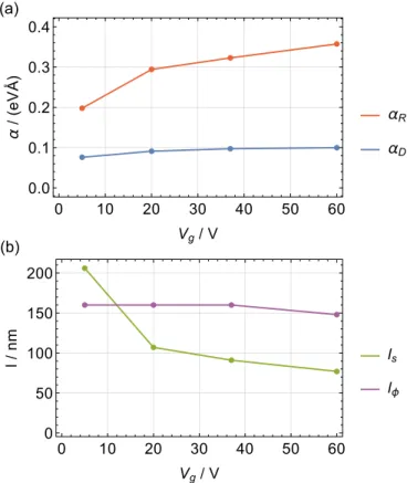
and possesses the following parameters. Adopting the findings of Ref. [38], the narrow band gap of InAs results in large Rashba and Dresselhaus SOC coefficients γR=117.1 e ˚A2 andγD=27.18 eV ˚A3, respectively. Moreover, the effective mass is given bym=0.026mewheremeis the bare electron mass [35]. In line with the experimental setup of Ref. [30], we consider a length of the nanowire of L=2.18μm and a radius ofR=47.5 nm. Moreover, we use the field-effect mobilityμ=600 cm2V−1s−1 and the 3D electron density n3D=5×1018cm−3. The change of the back-gate voltage Vg from 5 to 60 V yields an increase of the electron density by a factor of 1.5, whereas the mobility is assumed to remain relatively unchanged. By means of the relationsμ=eτe/m andkF =(3π2n3D)1/3, we find a mean-free pathle=vFτebe- tween 21 and 24 nm. Accordingly, ¯h/(Fτe) ranges from 0.14 to 0.18 and therefore theIoffe-Regelcriterion is generally well fulfilled.
Figure 3 depicts a gate-induced crossover from positive to negative relative magnetoconductanceGR≡G(B)− G(B=0), which is usually associated with a crossover from weak localization to weak antilocalization. The experiments are performed at a temperature ofT =4 K and the magnetic field is oriented perpendicular to the wire axis, i.e.,τB =τB,⊥
FIG. 3. Gate-controlled crossover from positive to negative relative magnetoconductance GR≡G(B)−G(B=0) in a doped 111 InAs nanowire. The symbol-dotted lines correspond to experimental data for different back-gate voltagesVg, which are fitted by theory (solid lines) using Eq. (21) and varying the Rashba and effective Dresselhaus SOC strengths as shown in Fig.4(a).
(cf. Sec. IX). In order to average out the superimposed universal conductance oscillations, each magnetoconductance curve represents the mean value of roughly 200 individ- ual measurements in 20-V gate-voltage intervals. We fitted Eq. (21) by changing the effective Dresselhaus parameterαD= γDk2F according to the modifications of the electron density and by adjusting the Rashba parameter αR, or equivalently the strength of the internal electric field |E|. The resulting electric field increases with the gate voltage from 1.7×10⁷to 3.1×10⁷ V/m. The Rashba and effective Dresselhaus SOC strengths are shown in Fig.4(a). A slight deviation from the typically expected linear Vg dependence of αR is attributed to deviations from a homogeneous electric field within the wire. We point out that the precondition for the zero-mode approximation,QsoR <1 is, strictly speaking, not perfectly fulfilled for large voltages. More precisely,QsoRranges from 0.64 to 1.16. However, by comparing the exact diagonalization with the zero-mode approximation (cf. Fig. 1), it becomes obvious that the most important characteristics of the spectrum, the minima, are barely changed and the application of the zero-mode approximation is here still justified. Furthermore, using the relationli =√
Deτi,i∈ {s,φ}, and 1/τs ≡(1/τs),+
as defined in Sec.VII[and in the limitQsoR1 in Eq. (17)], we can extract the spin relaxation and dephasing lengths ls and lφ, respectively, which are shown in Fig. 4(b). At Vg =5 V the spin relaxation lengthlsexceeds the dephasing lengthlφ, which reflects the observation of weak localization in Fig. 3. Hence, a controlled application of a gate voltage allows to reduce the spin relaxation length roughly by a factor of 3.
Critical discussion and comparison with previous results Hereafter, we follow with a critical discussion and compare our gathered data with previous experiments on similar n- doped InAs nanowire devices [15–18]. In these works, the
FIG. 4. Extracted fitting parameters for a doped 111 InAs nanowire. We show in (a) the Rashba and effective Dresselhaus SOC strengthαR and αD=γDk2F, and in (b) the spin relaxation and dephasing lengthls andlφ, respectively, in dependence of the back-gate voltageVg.
magnetoconductance data are analyzed by means of a 1D magnetoconductance formula [37], which does not consider the mesoscopic details of the system. In AppendixD, we use this formula to fit the magnetoconductance data of our device.
Aside from the obvious discrepancy between experimental data and theory, it shows disagreements with our findings above.
First, we remark that even for a vanishing back-gate voltage, a finite Rashba strengthαRwill remain, which was also seen in Refs. [15–18]. We attribute this to the fact that even for zero gate voltage an intrinsic electric field due to Fermi level surface pinning will remain. Aside from that, for small voltages other spin relaxation mechanisms can become important, above all, the Elliott-Yafet (EY) mechanism due to the large electron density through doping. However, we emphasize that the modification of the electron density in our sample alters the EY spin relaxation rate by a factor of 1.7 [55]. Since we detect an increase of the spin relaxation rate by a factor of 9.5, it is not possible to explain this behavior within EY theory.
Nevertheless, the strength of the extracted Rashba parameter αRshould be treated with caution as it comprises a contribution of additional spin relaxation rates.
Second, although similar transport parameters are found in Refs. [15–18], the variation of the dephasing length lφ
with the gate voltage in the according fits is most striking. In most of these works, the dephasing length increases with the gate voltage which is usually justified by a reduced electron-
electron interaction through an increase of the electron density.
Some authors even observed a decrease oflφwith increasing gate voltage [17] or oscillations [15]. It is most pronounced in Refs. [15,16,18], where the dephasing length suddenly changes by about 100 nm near the WL regime. In AppendixD, we show that the application of the 1D magnetoconductance formula of Ref. [37] to our nanowire device likewise leads to an unusual trend forlφ. This behavior is not seen in our device with our magnetoconductance model, where the dephasing length remains nearly constant. However, we find that in our model an unambiguous fitting of the magnetoconductance curve in the WL regime, in contrast to the WAL regime and opposed to the model in Ref. [37], is barely possible. Note that we could also fit for a lower value of lφ for Vg =5 V which would further increase the spin relaxation length and diminish the saturation value forαR. However, as we do not see any indication of a change oflφ in the WAL regime, we assume that a similar value holds in the WL regime. This finding supports the need of taking into account details on the mesoscopic scale of the nanowire as presented in this paper in order to obtain reliable transport parameters.
Based on our observations, we suggest that for dephasing the electron-electron interaction may be not as effective as previously assumed in a largely doped sample as considered here. This would be in agreement with the findings in disordered 3D metal films [56]. On the other hand, the change of electron density in our investigated system is possibly too low in order to make a reliable statement. Also, as the extracted dephasing length exceeds the diameter d of the wire, we expect the geometric properties to play an important role in a similar manner as it is the case for the magnetic dephasing. In planar quantum wires with a width smaller than the dephasing length electron-electron interaction has been identified as the predominant mechanism [57]. For further studies, we propose therefore (a) the development of a theoretical description of the inelastic scattering mechanisms as a function of temperature, electron density, and system size for a quasi-3D cylindrical wire and (b) an experimental investigation to see which mechanisms really apply. This would support a reliable parameter fitting in the WL regime and thereby enable a correct determination of the zero gate-voltage spin relaxation processes.
XII. SUMMARY AND PERSPECTIVE
We studied the effects of SOC on the quantum conductivity correction for semiconductor nanowires with zinc-blende structure. The spin relaxation due to Dresselhaus SOC is found to be the same for all spin components, independent of the wire growth direction and the wave vector of the spin density, and not affected by a change of the wire radius.
Contrarily, in presence of Rashba SOC the relaxation depends on the spin component. A homogeneous spin density that is polarized along the ˆx axis decays according to Eq. (17) if the wire radius is smaller than the spin precession length.
However, the long-lived spin states have helical structure in real space. Similarly to the planar wire [32], the relaxation due to Rashba SOC is strongly suppressed for small wire widths. Interestingly, a homogeneously excited spin density along the wire axis does not exhibit any dependence on the wire
radius and is therefore not subject to motional narrowing. The derived expressions for the magnetoconductance correction are fitted to the data of magnetoconductance measurements of a heavily doped back-gated InAs nanowire. We find good agreement between theory and experiment and reasonable transport parameters. For comparison, we also apply the 1D magnetoconductance formula of Kurdak et al. [37], which has been frequently used by other authors [9–11,13,15–18].
The fitted curves show larger deviations from the experi- mental observations and an unusual trend of the dephasing length.
We stress that the developed model holds for 3D-diffusive nanowires and a crossover to the quasiballistic regime is not included. For the latter case, it is plausible to assume that the Dresselhaus spin relaxation rate will decrease due to the reduction of the number of contributing channels as shown in Ref. [34] for planar wires. Additionally, the effects of surface roughness will start to play a noticeable role [47].
It is also to mention that semiconductor nanowires are often polytypic with zinc-blende and wurtzite segments or even pure wurtzite phase, even though the underlying semiconductor material has zinc-blende lattice in the bulk [28,58]. As the SOC in the wurtzite phase is fundamentally different, distinct characteristics concerning conductivity and spin relaxation can be expected and therefore further model calculations are strongly requested.
ACKNOWLEDGMENTS
We gratefully acknowledge K. Sladek and H. Hardtdegen for nanowire growth and we thank I. Otto for valuable experimental support. The authors also thank F. Dirnberger, D. Bougeard, A. Bringer, F. Mireles, and S. Csonka for useful discussions. This work was supported by Deutsche Forschungsgemeinschaft via Grants No. SFB 689 and No.
FOR 912.
APPENDIX A: RELATION BETWEEN TRIPLET BASIS AND SPIN DENSITY COMPONENTS
As shown in Ref. [33], there exists a unitary transformation between the spin diffusion equation and the Cooperon.
Therefore, we obtain an according transformation between the spin density s=(sx,sy,sz) and the triplet vector ˜s= (|1,1,|1,0,|1,−1)of the Cooperon, which is
˜s=Ucds, (A1)
with the unitary operator
Ucd =
⎛
⎜⎝
−1 i 0
0 0 √
2
1 i 0
⎞
⎟⎠ √
2. (A2)
APPENDIX B: SPIN MATRICES
The spin matrices of a system with two electrons in singlet- triplet basis|s,ms, with total spin quantum numbers∈ {0,1}
and according magnetic quantum numberms∈ {0,±1}, are
Sx= 1
√2
⎛
⎜⎝
0 0 0 0
0 0 1 0
0 1 0 1
0 0 1 0
⎞
⎟⎠,
Sy= i
√2
⎛
⎜⎝
0 0 0 0
0 0 −1 0
0 1 0 −1
0 0 1 0
⎞
⎟⎠,
Sz=
⎛
⎜⎝
0 0 0 0
0 1 0 0
0 0 0 0
0 0 0 −1
⎞
⎟⎠, (B1)
in the order {|0,0,|1,1,|1,0,|1,−1}. The singlet and triplet sectors are decoupled in this representation.
APPENDIX C: COOPERON HAMILTONIAN IN ZERO-MODE APPROXIMATION IN TERMS OF SPIN
DENSITY COMPONENTS
Relevant in experiments is the relaxation process of the spin densitys. Due to the gauge transformationUAthe eigenstates of the Cooperon HamiltonianHcdepend on the position on the cross section. We can write the triplet sector of the Cooperon Hamiltonian in the basis of the spin density components by reverting the gauge transformation after projecting the transformed Cooperon Hamiltonian on the zero mode and applying the basis transformation to the triplet sector as defined in AppendixA. More precisely, the triplet sector of the Cooperon Hamiltonian in the basis of the spin density components{sx,sy,sz}reads as in terms ofQ2so
⎛
⎝a d e d∗ b f e∗ f∗ c
⎞
⎠, (C1)
where
a=c−12 +12(aso−1) cos(2Qsox), b=c−12 −12(aso−1) cos(2Qsox), c=Q2z+λD+1,
d = −12(aso−1) sin(2Qsox), e= −2iQz(bso−1) sin(2Qsox),
f = −2iQz(bso−1) cos(2Qsox). (C2) Notably, for Qz=0 the sz component is decoupled and independent of the location on the wire cross section and the wire radius. Consequently, a spin density which is homogeneously polarized along the wire axis is not subject to motional narrowing in zero-mode approximation.
APPENDIX D: EXPERIMENTAL DATA FITTING WITH THE FORMULA OF KURDAKet al.
Here, we demonstrate the application of the 1D magneto- conductance formula of Kurdaket al. [37] to the nanowire device discussed in Sec.XI. This model is frequently used for
FIG. 5. (a) Gate-controlled crossover from positive to negative relative magnetoconductance GR≡G(B)−G(B=0) in a doped111InAs nanowire. The symbol-dotted lines correspond to experimental data for different back-gate voltagesVg, which are fitted by the 1D magnetoconductance formula of Kurdaket al.[37]
(solid lines), and adjusting the dephasing and spin relaxation lengths lφandls, as shown in (b).
the theoretical analysis of semiconductor nanowire devices [9–11,13,15–18]. In case of a diffusive wire of lengthL, the magnetoconductance correction reads as
G(B)= 2e2 h
1 2L
3
1 lφ2 + 4
3ls2 + 1 lB2
−1/2
− 1
lφ2 + 1 lB2
−1/2
, (D1)
with the dephasing, spin relaxation, magnetic dephasing length,lφ,ls, andlB, respectively. For the magnetic dephasing length, we used our relation for a perpendicular magnetic field, that is,lB =
DeτB,⊥ as derived in Sec. IXwhich is more appropriate for a cylindrical wire. Note that compared to the definition in Refs. [54,59], here alsolB ∝ |B|−1holds true. In Fig.5 we show the relative magnetoconductance correction GR=G(B)−G(0) and the accordingly obtained fitting parameters. Remarkably, in strong contradiction to the obser- vations using our model (cf. Sec.XI), the extracted dephasing length shows a monotonous decrease with the gate voltage which is rather unphysical. Also, the spin relaxation length is nearly twice as large for small gate voltages. Aside from
that, a strong discrepancy between the experimental data and theory in the weak antilocalization regime is obvious. As a
consequence of these observations, we suggest that a more appropriate model should be used.
[1] P. Yang, R. Yan, and M. Fardy,Nano Lett.10,1529(2010).
[2] A. B. Greytak, C. J. Barrelet, Y. Li, and C. M. Lieber,Appl.
Phys. Lett.87,151103(2005).
[3] J. Xiang, W. Lu, Y. Hu, Y. Wu, H. Yan, and C. M. Lieber,Nature (London)441,489(2006).
[4] P. Krogstrup, H. I. Jørgensen, M. Heiss, O. Demichel, J. V.
Holm, M. Aagesen, J. Nygård, and A. Fontcuberta i Morral, Nat. Photonics7,306(2013).
[5] X. Dai, S. Zhang, Z. Wang, G. Adamo, H. Liu, Y. Huang, C.
Couteau, and C. Soci,Nano Lett.14,2688(2014).
[6] X. Dai, A. Messanvi, H. Zhang, C. Durand, J. Eymery, C.
Bougerol, F. H. Julien, and M. Tchernycheva,Nano Lett.15, 6958(2015).
[7] Y. Oreg, G. Refael, and F. von Oppen,Phys. Rev. Lett.105, 177002(2010).
[8] V. Mourik, K. Zuo, S. M. Frolov, S. R. Plissard, E. P. A. M.
Bakkers, and L. P. Kouwenhoven,Science336,1003(2012).
[9] A. E. Hansen, M. T. Björk, I. C. Fasth, C. Thelander, and L.
Samuelson,Phys. Rev. B71,205328(2005).
[10] S. Dhara, H. S. Solanki, V. Singh, A. Narayanan, P. Chaudhari, M. Gokhale, A. Bhattacharya, and M. M. Deshmukh,Phys. Rev.
B79,121311(2009).
[11] X.-J. Hao, T. Tu, G. Cao, C. Zhou, H.-O. Li, G.-C. Guo, W. Y. Fung, Z. Ji, G.-P. Guo, and W. Lu,Nano Lett.10,2956 (2010).
[12] S. Estévez Hernández, M. Akabori, K. Sladek, C. Volk, S.
Alagha, H. Hardtdegen, M. G. Pala, N. Demarina, D. Grütz- macher, and Th. Schäpers,Phys. Rev. B82,235303(2010).
[13] I. van Weperen, B. Tarasinski, D. Eeltink, V. S. Pribiag, S. R.
Plissard, E. P. A. M. Bakkers, L. P. Kouwenhoven, and M.
Wimmer,Phys. Rev. B91,201413(2015).
[14] M. Kammermeier, P. Wenk, J. Schliemann, S. Heedt, and Th.
Schäpers,Phys. Rev. B93,205306(2016).
[15] P. Roulleau, T. Choi, S. Riedi, T. Heinzel, I. Shorubalko, T. Ihn, and K. Ensslin,Phys. Rev. B81,155449(2010).
[16] D. Liang and X. P. Gao,Nano Lett.12,3263(2012).
[17] Z. Scherübl, G. Fülöp, M. H. Madsen, J. Nygård, and S. Csonka, Phys. Rev. B94,035444(2016).
[18] K. Takase, Y. Ashikawa, G. Zhang, K. Tateno, and S. Sasaki, Sci. Rep.7,930(2017).
[19] M. Kammermeier, P. Wenk, and J. Schliemann,Phys. Rev. Lett.
117,236801(2016).
[20] J. Schliemann,Rev. Mod. Phys.89,011001(2017).
[21] M. Kohda and G. Salis,Semicond. Sci. Technol.32,073002 (2017).
[22] L. J. Lauhon, M. S. Gudiksen, D. Wang, and C. M. Lieber, Nature (London)420,57(2002).
[23] B. A. Wacaser, K. Deppert, L. S. Karlsson, L. Samuelson, and W. Seifert,J. Cryst. Growth287,504(2006).
[24] S. A. Fortuna and X. Li,Semicond. Sci. Technol.25,024005 (2010).
[25] S. Wirths, K. Weis, A. Winden, K. Sladek, C. Volk, S. Alagha, T. E. Weirich, M. von der Ahe, H. Hardtdegen, H. Lüthet al., J. Appl. Phys.110,053709(2011).
[26] C. Blömers, T. Rieger, P. Zellekens, F. Haas, M. I. Lepsa, H.
Hardtdegen, Ö. Gül, N. Demarina, D. Grützmacher, H. Lüth, and Th. Schäpers,Nanotechnology24,035203(2013).
[27] F. Haas, K. Sladek, A. Winden, M. von der Ahe, T. E. Weirich, T. Rieger, H. Lüth, D. Grützmacher, Th. Schäpers, and H.
Hardtdegen,Nanotechnology24,085603(2013).
[28] Z. Zhang, Z. Lu, H. Xu, P. Chen, W. Lu, and J. Zou,Nano Res.
7,1640(2014).
[29] S. d’Hollosy, M. Jung, A. Baumgartner, V. A. Guzenko, M. H.
Madsen, J. Nygård, and C. Schönenberger,Nano Lett.15,4585 (2015).
[30] S. Heedt, I. Otto, K. Sladek, H. Hardtdegen, J. Schubert, N. Demarina, H. Lüth, D. Grützmacher, and Th. Schäpers, Nanoscale7,18188(2015).
[31] M. Speckbacher, J. Treu, T. J. Whittles, W. M. Linhart, X. Xu, K. Saller, V. R. Dhanak, G. Abstreiter, J. J. Finley, T. D. Veal, and G. Koblmüller,Nano Lett.16,5135(2016).
[32] S. Kettemann,Phys. Rev. Lett.98,176808(2007).
[33] P. Wenk and S. Kettemann,Phys. Rev. B81,125309(2010).
[34] P. Wenk and S. Kettemann,Phys. Rev. B83,115301(2011).
[35] A. Bringer and Th. Schäpers,Phys. Rev. B83,115305(2011).
[36] V. E. Degtyarev, S. V. Khazanova, and N. V. Demarina,Sci. Rep.
7,3411(2017).
[37] Ç. Kurdak, A. M. Chang, A. Chin, and T. Y. Chang,Phys. Rev.
B46,6846(1992).
[38] R. Winkler,Spin-Orbit Coupling Effects in Two-Dimensional Electron and Hole Systems, Springer Tracts in Modern Physics, Vol. 191 (Springer, Berlin, 2003).
[39] I. Zutic, J. Fabian, and S. Das Sarma,Rev. Mod. Phys.76,323 (2004).
[40] M. Wu, J. Jiang, and M. Weng,Phys. Rep.493,61(2010).
[41] S. Hikami, A. I. Larkin, and Y. Nagaoka,Prog. Theor. Phys.63, 707(1980).
[42] P. Wenk and S. Kettemann, inHandbook on Nanophysics, edited by K. Sattler (CRC Press, Boca Raton, FL, 2010), p. 49.
[43] B. L. Al’tshuler and A. G. Aronov, Pis’ma Zh. Eskp. Teor. Fiz.
33, 515 (1981) [JETP Lett.33, 499 (1981)].
[44] I. L. Aleiner and V. I. Fal’ko, Phys. Rev. Lett. 87, 256801 (2001).
[45] J. S. Meyer, V. I. Fal’ko, and B. L. Altshuler, inNato Science Series II, Vol. 72, edited by I. V. Lerner, B. L. Altshuler, V. I.
Fal’ko, and T. Giamarchi (Kluwer, Dordrecht, 2002), p. 117.
[46] F. Wang, S. Yip, N. Han, K. Fok, H. Lin, J. J. Hou, G. Dong, T. Hung, K. S. Chan, and J. C. Ho,Nanotechnology24,375202 (2013).
[47] E. Khalaf and P. M. Ostrovsky, Phys. Rev. B 94, 165431 (2016).
[48] M. I. D’yakonov and V. I. Perel’, Fiz. Tverd. Tela13, 3581 (1971) [Sov. Phys.–Solid State13, 3023 (1971)].
[49] M. D’yakonov and V. Y. Kachorovskii, Fiz. Tekh. Poluprovodn.
20, 178 (1986) [Sov. Phys.–Semicond.20, 110 (1986)].
[50] S. V. Iordanskii, Yu. B. Lyanda-Geller, and G. E. Pikus, Pis’ma Zh. Eksp. Teor. Fiz.60, 199 (1994) [JETP Lett.60, 206 (1994)].
[51] F. G. Pikus and G. E. Pikus,Phys. Rev. B51,16928(1995).
[52] W. Knap, C. Skierbiszewski, A. Zduniak, E. Litwin-Staszewska, D. Bertho, F. Kobbi, J. L. Robert, G. E. Pikus, F. G. Pikus, S. V.
Iordanskiiet al.,Phys. Rev. B53,3912(1996).
[53] G. E. Pikus and A. N. Titkov, inOptical Orientation, Modern Problems in Condensed Matter Sciences, Vol. 8, edited by F.
Meier and B. P. Zakharchenya (North-Holland, Amsterdam, 1984).
[54] C. W. J. Beenakker and H. van Houten,Phys. Rev. B38,3232 (1988).
[55] J. N. Chazalviel,Phys. Rev. B11,1555(1975).
[56] J. J. Lin and J. P. Bird,J. Phys.: Condens. Matter 14, R501 (2002).
[57] K. K. Choi, D. C. Tsui, and K. Alavi,Phys. Rev. B36,7751 (1987).
[58] K. Hiruma, M. Yazawa, T. Katsuyama, K. Ogawa, K. Haraguchi, M. Koguchi, and H. Kakibayashi, J. Appl. Phys. 77, 447 (1995).
[59] S. Chakravarty and A. Schmid,Phys. Rep.140,193(1986).
![FIG. 1. Comparison of the zero-mode approximation (yellow) [Eqs. (12)–(14)] with the exact diagonalization of ˆ H c (blue) truncated to n max = 4 and | l max | = 4 for λ D = 0.1 and (a) Q so R = 0.3 and (b) Q so R = 1.5.](https://thumb-eu.123doks.com/thumbv2/1library_info/3943484.1533791/3.911.497.804.103.739/fig-comparison-zero-approximation-yellow-exact-diagonalization-truncated.webp)