Characterization of a Segmented n-Type Broad Energy Germanium Detector
Charakterisierung eines Segmentierten Broad Energy Germanium Detektors
Technische Universit¨at M¨unchen
Master’s Thesis
by
Martin Schuster
6. Dezember 2016
First referee: Prof. Dr. Allen Caldwell
Second referee: Prof. Dr. Lothar Oberauer
Supervisor: Dr. Iris Abt
Contents
1. Introduction 5
2. Motivation 7
3. Semiconductor Detectors 9
3.1. Charge Carrier Creation . . . . 9
3.2. Impurities and Doping . . . . 10
3.3. pn Junction and Depletion . . . . 10
3.4. Germanium Detectors . . . . 11
3.5. Broad Energy Germanium (BEGe) Detectors . . . . 11
3.6. Pulse Formation . . . . 11
3.7. Operational Characteristics . . . . 15
3.7.1. Leakage Current . . . . 15
3.7.2. Charge Collection Time . . . . 15
3.7.3. Incomplete Charge Collection . . . . 16
3.7.4. Energy Resolution . . . . 16
4. The Segmented BEGe Detector under Study 17 5. Experimental Setup 21 5.1. The Detector and Cryostat . . . . 22
5.2. Data Acquisition System . . . . 23
5.3. Data Taking . . . . 24
6. Signal Processing 25 6.1. Baseline and Pulse Decay . . . . 25
6.2. Pulse Amplitude Determination . . . . 27
6.2.1. Fixed Window Method . . . . 27
6.2.2. Sliding Window Method . . . . 27
6.2.3. Results . . . . 28
6.3. Reconstructing the Deposited Energy . . . . 31
6.3.1. Procedure for cross-talk correction and energy calibration . . . . 32
6.4. Check of the Cross-Talk Correction and Energy Calibration Procedure . . . . . 37
6.5. Energy Resolutions . . . . 40
7. Detector Characteristics 41 7.1. Segment Boundaries . . . . 41
7.2. Crystal Axes . . . . 46
7.3. Event Localization . . . . 47
Contents
7.5. Multi-Site Event vs. Single-Site Event Discrimination . . . . 55
8. Summary and Outlook 61
A.
133Ba-Data Sets 63
A.1. Top-Scans . . . . 63 A.2. Side-Scans . . . . 72
B.
60Co- and
228Th-Data Sets 77
4
1. Introduction
Neutrinos play an important role in our universe. They are nearly as abundant as photons, yet they still pose unanswered fundamental questions. According to the original Standard Model, SM, neutrinos were massless elementary particles. Neutrino oscillation experiments, however, give evidence for a finite neutrino mass. They provide information on the di ff erences between the squared masses, but the absolute mass scale as well as the very nature of the neutrino (Dirac- or Majorana-particle) remain unknown [1]. Targeting those questions experimentally proves challenging.
One of the ways to address both topics is the search for neutrinoless double beta decay, 0νββ.
If it occurs, the neutrino is its own anti-particle. The mass of such a Majorana neutrino, m
ee, could be derived from the half-life of the decay, assuming that it is the only particle exchanged in such decays [2].
Germanium is one of the elements that is usually employed in 0νββ searches. Its isotope
76Ge is a candidate for 0νββ. Neutrino accompanied double beta decay, 2νββ, has already been ob- served [3] [4]. As a semiconductor, germanium can act as source and detector at the same time, which yields a high detection e ffi ciency. Due to the extreme rarity of the expected events, the background has to be extremely low. Segmentation of HPGe (High Purity Germanium) de- tectors can potentially contribute to the rejection of background events [5]. Thus, segmented detectors are interesting, especially with regard to a future ton-scale 0νββ germanium experi- ment. The excellent energy resolution of HPGe detectors and their capability to resolve γ lines from several keV to several MeV also make them the tool of choice for many other applications.
In Chapter 2, the study presented in this thesis is motivated by discussing some physics as- pects of future experiments.
The general working principle of semiconductor detectors and HPGe Detectors in particular is covered in Chapter 3.
In Chapter 4, the segmented BEGe (Broad Energy Germanium) detector, which is the research object in this thesis, will be introduced.
The experimental setup, including the detector and the data acquisition system, as well as the data taking procedure, is described in Chapter 5.
Data processing is described in Chapter 6. This includes a study on the optimization of the pro- cedure to calculate the amount of deposited energy from the recorded pulse-shape of an event.
Chapter 7 presents the characterization of the segmented BEGe detector, including the determi- nation of the segment boundaries, the dependence of the charge drift-times on the crystal axes and the behavior of the contact and passivation areas. The special capabilities of this kind of detector regarding the identification of Single-Site Events, SSiteEs, versus Multi-Site Events, MSiteEs, as well as the reconstruction of event topologies will also be discussed.
The thesis closes with Chapter 8 where the results are summarized and an outlook to further
investigations and applications is provided.
2. Motivation
Neutrinoless double beta decay, if observed, can provide information on the absolute neutrino mass scale and establish the Majorana nature of neutrinos. Observing such a fundamental pro- cess, which violates the Lepton number conservation by two, may provide hints about the mech- anism that resulted in the particle-antiparticle asymmetry and, thus, the matter dominance in the universe [6].
If some isotope, X, decays via 2νββ, two neutrons are converted to two protons, and two elec- trons, e
−, are emitted alongside two electron-antineutrinos, ν
e[7]:
A
Z
X →
AZ+2X + 2e
−+ 2ν
e, (2.1)
where A refers to the atomic mass and Z refers to the atomic number. In case of 0νββ, no neutrinos are emitted:
A
Z
X →
ZA+2X + 2e
−. (2.2)
Figures 2.1a and 2.1b show the respective Feynman diagrams. Figure 2.1c shows the expected 2 e
−spectrum in the presence of both processes. Since the total energy is distributed between the electrons and the neutrinos, the spectrum for 2νββ is continuous. In the case of 0νββ, the energy is only distributed between the two electrons. The total energy is deposited in the detector and gives rise to a peak at Q
ββ. As a follow up to the GERDA [8] and MAJORANA [9]
experiments, which search for 0νββ using
76Ge HPGe Detectors, a joint e ff ort to develop a ton- scale experiment using similar techniques is under consideration. The large exposure of such an experiment requires a background level at the order of 10
−5counts / kg / keV / year in the Region of Interest, RoI. The best background level so far of 0.7
+−0.51.1· 10
−3was achieved by the GERDA collaboration [10]. The RoI for
76Ge based 0νββ searches is centered around 2039 keV, which corresponds to the Q
ββ-value of the 2νββ. There are two general principles to achieve a lower background [11]:
(a) (b) (c)
Figure 2.1.: (a) Feynman diagram for 2νββ. (b) Feynman diagram for 0νββ. (c) Expected spec-
trum in the presence of both processes. The 0νββ peak height is not to scale. Figures
2. Motivation
• Avoid background: Sophisticated shielding against all types of radiation is employed.
Deep underground laboratories to reduce the e ff ect of cosmic muons are necessary. In order to avoid cosmic activation, all relevant materials should be processed and stored underground. This includes crystal growth and storage, and detector manufacturing. Ad- ditionally, the supporting structures should have a low activity and mass, and the material close to the detectors should be minimized in general.
• Recognize Background: It is impossible to completely avoid background. In order to further decrease the background level, intelligent detectors and analysis methods are em- ployed. Examples are event classification and pulse-shape analysis.
Signal events will be Single-Site Events, SSiteEs, since the two electrons deposit their energy very locally.
A dominant source of background for the RoI are high energy photons, e.g. originating from the radioactive decay of
228Th to
208Tl [12]. The main interaction mechanism for photons with mat- ter in this energy range is Compton scattering [13]. Upon scattering, the energy is transferred to an electron which leaves the atom with a kinetic energy equal to the transferred energy minus the ionization energy. It deposits its energy locally. Most of the time the high energy photon will interact several times at di ff erent locations within the detector, each time transferring only part of its energy. Such an event is called Multi-Site Event, MSiteE.
While the sum of the energies of the depositions may lie in the RoI and mimic a signal event, it can be rejected as background if one can identify it as an MSiteE. The capability of a detector to di ff erentiate between SSiteEs and MSiteEs is therefore an important property. One method to identify and reject MSiteEs is based on pulse-shape analysis and is discussed in Chapter 7.
Segmentation of an HPGe detector can also contribute to the identification MSiteEs in a simple and robust way. If the energy depositions of an event occur in di ff erent segments it is classified as an MSiteE [14] [15].
Especially in searches for rare events, for which really strict requirements have to be met, a precise understanding of the detector and its response is crucial. Research on HPGe detec- tors to increase the knowledge about such devices and to facilitate the development of new intelligent detectors is an important part of the research and development program for many experiments [16]. The complete understanding of the detectors will be essential for a future germanium-based ton-scale experiment.
8
3. Semiconductor Detectors
In this section, the general working principle of semiconductor detectors, as well as operational characteristics and relevant phenomena are briefly discussed. More in-depth information on these topics can be found in literature [13].
Crystalline materials exhibit a periodic lattice structure. This feature introduces so called en- ergy bands. In a pure material, electrons are confined to one of two bands, either the valence band, or the conduction band. The energy gap that separates those bands is called the band-gap.
Materials are classified according to the size of their band-gap. Insulators usually have a band- gap larger than 5 eV, while semiconductors show a band-gap of the order of 1 eV. Electrons in the valence band correspond to electrons which are bound to the atom at the lattice site, while electrons in the conduction band are free to migrate through the crystal and therefore add to the conductivity of the material.
3.1. Charge Carrier Creation
Thermal excitation leads to electrons being elevated from the valence to the conduction band.
A so called electron-hole pair is created. A hole is a vacancy where an electron is missing and introduces a positive charge. Upon applying an electric field, the electrons and holes will drift in opposite directions. In the absence of such a field, the electron will eventually recombine with the hole. The following equation gives the probability per unit time that an electron-hole pair is generated thermally [13]:
p(T ) = CT
3/2exp − E
g2kT
!
. (3.1)
Here, T is the absolute temperature, E
gis the band-gap energy, k is the Boltzmann constant and C a material specific constant.
Equation. 3.1 implies that the equilibrium between electron-hole pair generation and recombi- nation is strongly dependent on the temperature and the band-gap energy. Cooling down the crystal will shift the equilibrium towards fewer electron-hole pairs.
When a charged particle traverses the crystal, it creates electron-hole pairs along its path. The
amount of energy, which is necessary to create one electron-hole pair is referred to as ionization
energy, . The small values of , typically < 5 eV, are important for the intrinsically good en-
ergy resolution of semiconductor detectors. The large number of charge carriers provides better
statistics than the less e ffi cient sampling detectors.
3. Semiconductor Detectors
3.2. Impurities and Doping
In reality, pure crystals do not exist. Even after the most sophisticated purification processes, one is left with residual impurities. The impurities dominate the electric properties of a crystal.
Typically, electrically active impurities are intentionally introduced to a crystal to engineer these properties. If some other element takes the place of a normal atom in the lattice of a crystal of group IV atoms, typically Si or Ge, one refers to it as a substitutional site:
• n-Type: If the substitute atom is from group V like phosphor, it is called donor because it has five valence electrons as opposed to four of the ordinary atom. This results in an excess electron after all covalent bounds have been formed. This electron is only loosely bound and it takes little energy to elevate it to the conduction band. By thermal excitation, a large percentage of the donor impurities will be ionized at any time. In this case, the electrons are the majority carriers and provide the dominant contribution to the conductivity. The holes are called minority carriers.
• p-Type: Contrary to the n-type, the substitutional site will be occupied by an acceptor impurity, e.g. an element from group III of the periodic table, like boron. Having only three valence electrons, one covalent bond with its neighbors is left unsaturated. This introduces an excess of holes, which are the majority carriers and thus the dominant contribution to the conductivity. In this case, the electrons are the minority carriers.
3.3. pn Junction and Depletion
Even though doped materials feature an excess in electrons or holes, respectively, they are in- trinsically not electrically charged. However, when p- and n-doped crystals are brought to good thermodynamic contact a so called space-charge region is formed. The excess charge carriers start to di ff use across the junction and build up a net charge. The resulting electric field counter- acts the di ff usion. An equilibrium between electrical drift and particle di ff usion is established.
The p-doped side of the junction is negatively charged while the n-doped side is positively charged. Any newly generated electron-hole pair in the space charge region is separated by the electric field and the charge carriers are swept to the respective side of the junction. Since this process is much faster than the thermal generation of charge carriers, the steady-state concen- tration of electrons and holes is strongly diminished. The region is called depleted. The charge carriers generated by ionizing radiation can be detected.
The crystal with a pn junction is a diode. Applying a reverse bias increases the electric potential.
The drift speed is increased and the depletion happens more swiftly. Additionally, the depletion region, which corresponds to the active volume of the detector, broadens. In case of an n-type detector a large part of the detector, the bulk, will be n-doped. The p-doped region is small in comparison. A positive voltage is applied to the n side. The majority carriers are hindered from crossing the junction which greatly increases the resistivity.
10
3.4. Germanium Detectors
3.4. Germanium Detectors
Germanium detectors are predominantly used to detect γ radiation up to a couple of MeV.
The detection of such deeply penetrating radiation requires the detectors to have a thick active volume. The thickness of the depletion region is given by
d = 2 ·
d· U
biase · N
!
1/2, (3.2)
where
dis the dielectric constant, U
biasis the reverse bias voltage, e the electric charge and N the net impurity concentration in the bulk of the semiconductor material. The limit on the depletion depth for detectors fabricated from silicon or germanium with usual levels of impu- rities is given by U
bias, which must be kept below the breakthrough voltage. Thus, in order to build thicker detectors with a given U
bias, the net impurity concentration has to be reduced.
Germanium can be refined to impurity levels as low as 1 part in 10
12, corresponding to approxi- mately 10
10atoms / cm
3. Using this ultrapure material, detectors with depletion depths of several centimeters are available.
3.5. Broad Energy Germanium (BEGe) Detectors
BEGe detectors are cylindrical detectors with a small contact area on one of the end-plates of the cylinder. They are capable of resolving γ-lines from 3 keV up to 3 MeV [17]. The n-type detector under study was produced by CANBERRA France. It has an n
+contact on one end- plate, surrounded by a passivated ring. The rest of the surface called mantle is segmented in four p
+electrodes. A detailed description is given in Sec. 4. BEGe detectors are currently employed in GERDA Phase II [8].
3.6. Pulse Formation
The contacts of germanium detectors are created by introducing high electrically active impurity concentrations on the surfaces. A p-type (p
+) contact is created e.g. via boron implantation. An n
+contact is formed e.g. by lithium di ff usion. The voltage is applied across these contacts which form the electrodes of the detector.
In germanium detectors, where electron- and hole- mobilities are similar, both types of charge carriers contribute to the output pulse. The charges drift along the electric field lines and in- fluence charges in the contacts. The charges are integrated by charge-sensitive amplifiers. Ac- cording to the Shockley-Ramo theorem [13][18], the charge, Q, that is induced on an electrode can be written as
Q = qφ
0(~ x) , (3.3)
where q is the charge of the carriers, and φ is the so called weighting potential. The weighting
3. Semiconductor Detectors
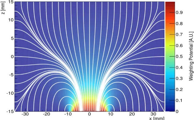
to unity, while the potentials for all other electrodes are set to 0. The weighting potential is not the real electric potential but is used to calculate Q. It takes into account that charges far away from the electrode contribute less to Q than charges close by. The integrated charge induced is independent on the location of the charge carrier generation and energy conservation is fulfilled. Figure 3.1 shows two typical pulses as recorded for the n
+(core) and one of the p
+electrodes (segments) of the BEGe detector investigated for this thesis. Figure 3.2 shows the weighting field of the core of this detector. It varies rapidly close to the core-contact. As a result, the drift speed of the charge carriers rapidly changes near the contact. The charge- sensitive amplifier for the core records a rapidly increasing charge until the charge is collected.
The slow rise of the core (n
+)-contact pulse at the beginning is typical for BEGe detectors. The pulses as observed on the n
+and p
+electrodes are quite di ff erent. Note that also non-collecting mantle-electrodes can have charges induced due to their weighting potentials. The resulting pulses are called mirror pulses, see Fig 3.3. The charge collection time varies significantly depending on the location of the energy deposition. If the deposition occurs near the n
+contact, the electrons will be collected very quickly, while the holes have to drift across the bulk of the detector to reach the p
+contact. Due to the large volume and inhomogeneous electric field, charge collection times as long as 2-3 µs occur.
12
3.6. Pulse Formation
Time [ns]
0 2000 4000 6000 8000 10000 12000 14000 16000 18000 20000
Induced Charge [ADC]
0 100 200 300 400
Charge Collection Time
Core
(a) A typical core (n
+) electrode pulse of the BEGe detector investigated for this thesis. The charge collection time is ≈ 850 ns.
Time [ns]
0 2000 4000 6000 8000 10000 12000 14000 16000 18000 20000
Induced Charge [ADC]
0 50 100 150 200 250 300
350
Seg. 4
(b) The corresponding pulse recorded at the p
+electrode of segment 4.
Figure 3.1.: The event originates from a
60Co data set. The electrons drift towards the n
+, the
holes drift towards the p
+electrode. The energy of the deposition is proportional to
the maximum pulse height. For a detailed discussion, see Sec. 6.
3. Semiconductor Detectors
Figure 3.2.: Cross-section of a BEGe detector. The weighting potential is color coded. The drift path of the charge carriers is indicated by the white lines. The field calculations were performed using the software package MAGE [19].
Time [ns]
0 2000 4000 6000 8000 10000 12000 14000 16000 18000 20000
Induced Charge [ADC]
−15
−10
−5 0 5 10 15
20
Seg. 3
Figure 3.3.: Mirror pulse in the non-collecting segment 3 corresponding to the core and seg- ment 4 pulses shown in Figs. 3.1a and 3.1b. The pulse is first dominated by positive charge carriers, then for a short time by electrons before again the positive charges dominate. This reflects the respective distances of the charge carriers to segment 3.
14
3.7. Operational Characteristics
3.7. Operational Characteristics
In this section, some of the phenomena occurring in germanium detectors are described. Under- standing their origin and knowing how to handle them is important to achieve a good detector performance.
3.7.1. Leakage Current
Applying a reverse bias voltage to a junction gives rise to a small current of the order of a couple of picoampere, the leakage current. There are two contributions to this current:
• The bulk leakage current occurs within the detector volume. Once the depletion region is established, the majority carriers are rejected from the junction. However, minority carri- ers, which are continuously generated on either side of the junction are attracted and may pass freely. This leads to a small and in most cases insignificant current. Another con- tribution to bulk leakage current stems from the thermally generated electron-hole pairs within the depletion region. The single countermeasure is cooling the material. Espe- cially germanium, due to its small band gap energy, can only be operated at temperatures around 100 K in order to su ffi ciently suppress thermal electron-hole pair generation.
• Surface leakage current arises at the junction edges, where high voltage gradients are present. The magnitude of the surface leakage depends strongly on the quality of the relevant detector surfaces (passivation) and their cleanliness. Exposure to humidity or fingerprints can increase surface currents significantly. Also important is the quality of the vacuum in which the detector is operated.
Monitoring the leakage current is common practice, as a low and constant leakage current is an indicator of good detector performance. The precise value of the leakage current depends on the detector design.
3.7.2. Charge Collection Time
The charge collection time defines the pulse length. There are two contributions to the charge collection time:
• Drift time: When incident radiation forms electron-hole pairs, it takes time for them to migrate from the point of creation to the electrodes. This time depends on the strength of the electric field and on the distance as well as on the thickness of the depletion region.
Typical drift times for BEGe detectors range from a couple of hundred nanoseconds up to 2-3 µs.
• Plasma time: Especially for heavy charged particles such as alphas or fission fragments,
the electron-hole pair density is high enough to form a plasma-like cloud. The interior of
this cloud is shielded from the influence of the electric field and at first, only the outer part
will start to drift. Once the cloud is su ffi ciently dispersed, also the previously shielded
charge carriers will move. The plasma time is basically the delay until the plasma-like
particle cloud disperses. For the studies presented in this thesis, the plasma time is irrele-
3. Semiconductor Detectors
3.7.3. Incomplete Charge Collection
During their drift through the detector, the charge carriers can be stopped such that they cease to contribute to the output pulse. Metallic atoms such as zinc or aurum, that are occupying substitutional sites and introduce energy levels near the middle of the band-gap, are referred to as deep impurities. They act as charge traps or recombination centers and are limiting the lifetime of electrons and holes:
• Charge Trapping: When a charge carrier is captured in a deep impurity site it may stay there for a comparably long time. Although it might ultimately be released again, it does not further contribute to the pulse since the observation of the charge collection process has already ended.
• Recombination Center: Recombination centers can capture both holes and electrons.
Most recombination processes occur via the energy levels introduced by such impurities, rather than recombining across the full width of the band-gap. The recombined charges are lost for the charge collection process.
These e ff ects intrinsically scale with the charge collection time. This is the time it takes for the charge carriers to reach the electrodes and is derived from the drift distance and the drift speed. For a good detector performance, close to 100% of the charge carriers should be collected. The charge collection time should therefore be much shorter than the mean lifetime.
The impurity level has to be su ffi ciently low to ensure a mean lifetime of ≈ 10 µs since charge collection times are usually less than ≈ 3 µs [13].
3.7.4. Energy Resolution
The excellent energy resolution for γ-rays, especially compared to e.g. NaI(Ti) scintillators, is the determining attribute of germanium detectors [20]. Three main factors contribute to the overall energy resolution. Its Full Width Half Maximum, FW H M, can be written as:
FW H M
2= W
2stat+ W
coll2+ W
el2, (3.4) where the respective W values are the widths associated with the following three mechanisms:
• The first term, W
stat, refers to the intrinsic statistical fluctuations of the number of charge carriers created by the incident radiation:
W
stat2= (2.35)
2· F · · E , (3.5) where F is the Fano factor, which is approximately 0.12 for Germanium and describes the ratio between the observed variance to the Poisson predicted variance. The other parameters are the energy which is necessary to create one electron-hole pair, , and the total Energy deposited by the γ-ray, E. In germanium ≈ 2.96 eV [13].
• The second term, W
coll2, is due to incomplete charge collection, see Sec. 3.7.3.
• The third contribution, W
el2, denotes the e ff ect of the electronics. It is, in contrast to the former two, independent of the registered energy. Typically, it is measured by connecting the output of a pulse generator to the preamplifier.
Which of the three contributions dominates is dependent on the size of the energy deposit and on detector parameters, such as size, type, impurity level, leakage current and surface quality.
16
4. The Segmented BEGe Detector under Study
BEGe detectors are interesting devices due to their complex weighting potential. The mantle of the device under study was segmented to allow the detailed study of such a device. Segmented detectors give information on the azimuthal positions of energy depositions and feature a sim- ple and robust way to identify multiple energy deposits. This allows cross-checks for methods purely relying on pulse-shape analysis.
The segmented BEGe, sBEGe, introduced here is a prototype detector, which was designed in the GeDet group and manufactured by CANBERRA France. It features the basic concepts of a BEGe, while introducing four mantle segments, see Fig. 4.1. The segment 1, 2 and 3 electrodes cover equal areas, while the segment 4 electrode covers the remaining surface - apart from the passivation and core-contact area. The surface covered by the segment 4 electrode is about three times larger than the area of each other segment. This design introduces the minimum number of additional readout channels to provide φ information about the energy depositions.
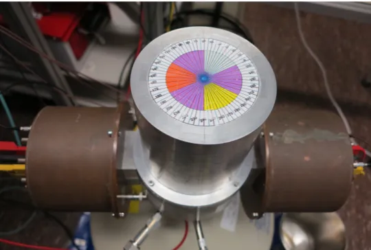
The passivation layer protects the germanium from oxidation. The sBEGe is an n-type detec- tor which is operated with a high voltage of + 4500 V. Its dimensions are 40 mm in height and 75 mm in diameter. The passivation layer extends to a diameter of 39 mm and the core-contact has a diameter of 15 mm.
The detector was installed in the K1-cryostat, see Fig. 4.2, with the passivation and contact area facing the top of the cryostat. The detector was accidentally installed with a slight tilt, which must be taken into account for certain parts of the analysis. For top-scans the e ff ect is
(n+Corecontact)
75 mm 15 mm
(a) End-plate with n
+contact.
Segment 1
Segment 2 Segment 3
Segment 4
(b) Layout of the segments.
Figure 4.1.: The design of the sBEGe [19].
4. The Segmented BEGe Detector under Study
Figure 4.2.: The K1-cryostat containing the detector. The scan-coordinate reference sheet, which was used to perform the top-scans, also shows the location of the color coded segments. The complete setup is described in Sec. 5.
corrected by taking into account the decentralization and rotational shift of the detector center in the xy-plane, the tilt relative to the z-axis is neglected. The detector is located, relative to the cryostat coordinates, at x = − 1 mm, y = 3 mm and φ = 2.3
◦. The cryostat coordinates are from here on referred to as scan coordinates, see Figs. 4.2 and 4.3.
18
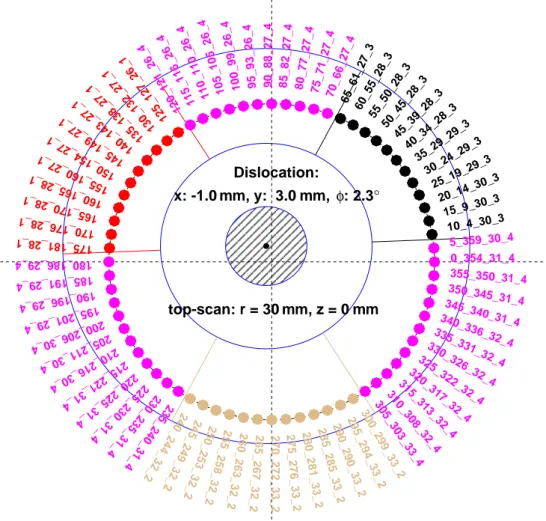
0_354_31_4 5_359_30_4 10_4_30_3 15_9_30_3 20_14_30_3 25_19_29_3 30_24_29_3 35_29_29_3 40_34_28_3 45_39_28_3 50_45_28_3 55_50_28_3 60_55_28_3 65_61_27_3 70_66_27_4 75_71_27_4 80_77_27_4 85_82_27_4
90_88_27_4
95_93_26_4 100_99_26_4105_105_26_4 110_110_26_4 115_116_26_4 120_121_26_4 125_127_26_1 130_132_27_1 135_138_27_1 140_143_27_1 145_149_27_1 150_154_27_1 155_160_27_1 160_165_28_1 165_170_28_1 170_176_28_1 175_181_28_1 180_186_29_4 185_191_29_4 190_196_29_4
195_201_29_4 200_206_30_4
205_211_30_4 210_216_30_4
215_221_31_4 220_225_31_4
225_230_31_4 230_235_31_4
235_240_31_4 240_244_32_2
245_249_32_2 250_253_32_2 255_258_32_2 260_263_32_2 265_267_32_2 270_272_33_2 275_276_33_2 280_281_33_2285_285_33_2290_290_33_2295_294_33_2300_299_33_2305_303_33_4310_308_32_4315_313_32_4320_317_32_4
325_322_32_4 330_326_32_4
335_331_32_4 340_336_32_4
345_340_31_4 350_345_31_4
355_350_31_4
Dislocation:
° : 2.3 φ m, m m, y: 3.0 m
x: -1.0
m m m, z = 0 m
top-scan: r = 30
Figure 4.3.: Schematic of the dislocation of the detector inside the K1-cryostat. The intersection
of the dashed lines indicates the center of the cryostat. The colored points indicate
the impact positions of a source for a r = 30 mm top-scan. Each point is labeled
with four numbers. The inner number refers to the φ position in scan-coordinates,
the second number gives the φ position in detector coordinates. The third number
is the radius in detector coordinates and the outer number indicates the segment.
5. Experimental Setup
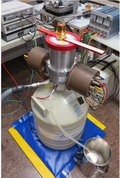
The experimental Setup is shown in Fig. 5.1. The yellow foam mat and the pair of sandbags decouple the detector setup from the ground. This way microphonic noise is e ff ectively reduced.
On top of the sandbags sits the liquid nitrogen, LN
2, dewar. The cryostat, in which the detector is mounted, rests on top, as the attached copper cooling finger is dipped into the LN
2. In the background to the right, one can see the power supply unit for the preamplifier boards supplying 24 V at 0.5 A.
Figure 5.1.: The experimental setup during the top-scans. A collimated
133Ba source rests on
the support structure, which allows the positioning of the source in the xy-plane.
5. Experimental Setup
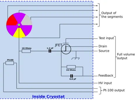
1G Ohms 1.2 nF
1G Ohms
0.8 pF
Output of the segments
Test input Drain Source
Feedback HV input
Full volume output
Pt100
Pt-100 output
Inside Cryostat JFET
(a) Schematic of the detector read-out [19].
(b) Feed-throughs in the K1-cryostat.
Figure 5.2.: Schematics of the detector read-out and K1-cryostat feed-throughs.
5.1. The Detector and Cryostat
The detector and the K1-cryostat were introduced in the previous chapters. The copper ears contain the preamplifiers for the four segments on the right side, and the core preamplifier as well as the HV- connector on the left side. Figure 5.2 provides schematics of the detector read- out and cryostat feed-throughs. As indicated in Fig. 5.2a, the JFET of the core preamplifier is installed inside the cryostat and thus cooled.
22
5.2. Data Acquisition System
5.2. Data Acquisition System
The data acquisition system, DAQ, used for all the measurements was produced by STRUCK.
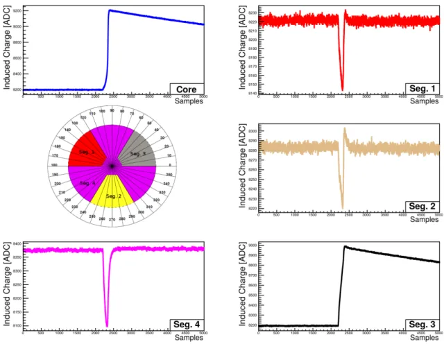
The DAQ features a sampling rate of 250 MHz, resulting in one sample every 4 ns. For each event, 20 µs of pulse data are stored for each read-out channel. An event as recorded for the segments and the core is shown in Fig. 5.3.
Figure 5.3.: Pulses for all the segments of an event in segment 3. Distinct mirror pulses are
observed for all non-collecting segments.
5. Experimental Setup
5.3. Data Taking
Three di ff erent sources were used for data taking, a
133Ba, a
60Co and a
228Th source. The
133Ba- source, featuring low keV γ-lines, was used to study the detector surface and the behavior of charge carriers in and near the passivation and the core-contact area. It was also used to characterize the detector in general. The
60Co and
228Th sources were uncollimated. These sources provide data distributed over the bulk of the detector. The data sets are listed in Tab. 5.1 and described in detail in the appendices.
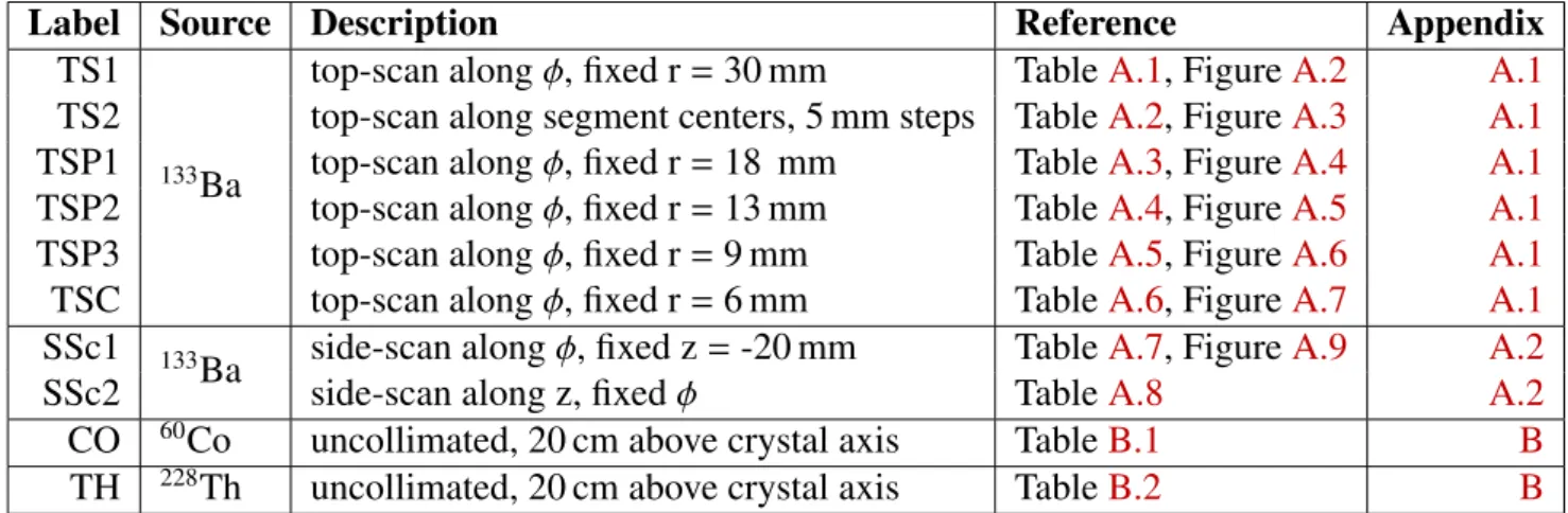
Label Source Description Reference Appendix
TS1
133
Ba
top-scan along φ, fixed r = 30 mm Table A.1, Figure A.2 A.1 TS2 top-scan along segment centers, 5 mm steps Table A.2, Figure A.3 A.1 TSP1 top-scan along φ, fixed r = 18 mm Table A.3, Figure A.4 A.1 TSP2 top-scan along φ, fixed r = 13 mm Table A.4, Figure A.5 A.1
TSP3 top-scan along φ, fixed r = 9 mm Table A.5, Figure A.6 A.1
TSC top-scan along φ, fixed r = 6 mm Table A.6, Figure A.7 A.1
SSc1
133Ba side-scan along φ, fixed z = -20 mm Table A.7, Figure A.9 A.2
SSc2 side-scan along z, fixed φ Table A.8 A.2
CO
60Co uncollimated, 20 cm above crystal axis Table B.1 B
TH
228Th uncollimated, 20 cm above crystal axis Table B.2 B
Table 5.1.: Data sets taken with the three sources. The detailed tables plus figures are given in the appendices as listed.
24
6. Signal Processing
The Data Acquisition System, DAQ, records the run-time and event-by-event pulses for all segments and the energy as determined online. The DAQ files are converted to ROOT-files in order to prepare the data for script based processing with ROOT. In order to optimize the resolution, the online energy determination was not used. Instead, studies to optimize the pulse amplitude determination were performed and the pulse amplitudes were calculated o ffl ine. The pulse processing and energy calibration procedure are described in the following subsections.
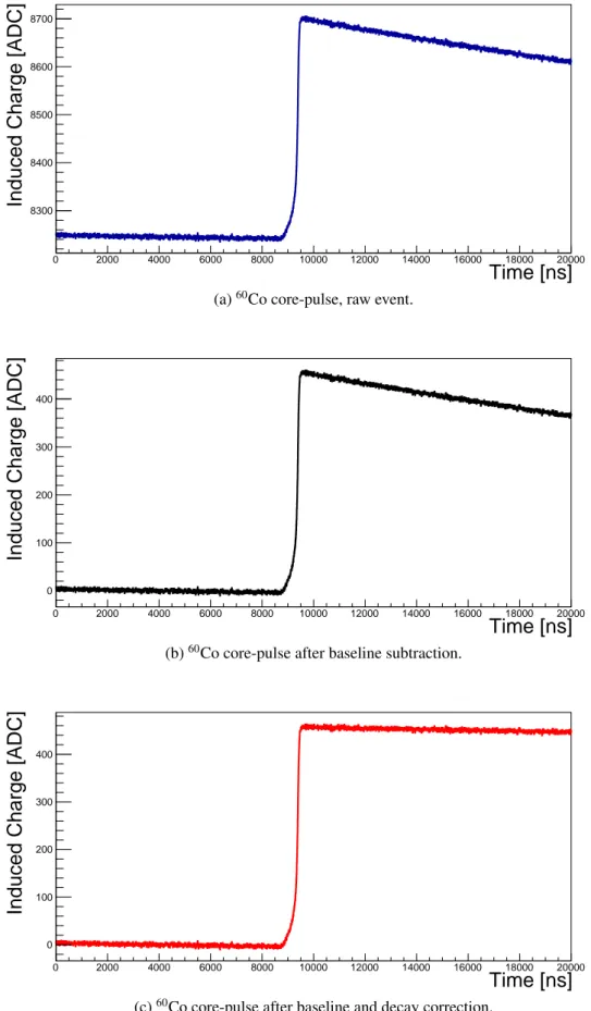
6.1. Baseline and Pulse Decay
Figure 6.1a shows a typical core pulse as recorded by the DAQ. As a first step, the pulse baseline is adjusted to zero. The resulting pulse is shown in Fig. 6.1b. A pulse reaches its maximum, the amplitude, when all charge carriers are collected. Afterwards, it decays exponentially with a time constant depending on the configuration of the amplifier. The energy is proportional to the amplitude. In the presence of noise, the amplitude can be determined more precisely, if the pulse is first corrected for its decay.
Figure 6.1c shows the pulse after the pulse-decay correction. These steps are applied to the
pulses of all segments for every event.
6. Signal Processing
Time [ns]
0 2000 4000 6000 8000 10000 12000 14000 16000 18000 20000
Induced Charge [ADC]
8300 8400 8500 8600 8700
(a)
60Co core-pulse, raw event.
Time [ns]
0 2000 4000 6000 8000 10000 12000 14000 16000 18000 20000
Induced Charge [ADC]
0 100 200 300 400
(b)
60Co core-pulse after baseline subtraction.
Time [ns]
0 2000 4000 6000 8000 10000 12000 14000 16000 18000 20000
Induced Charge [ADC]
0 100 200 300 400
(c)
60Co core-pulse after baseline and decay correction.
Figure 6.1.: Stages of the pulse processing to prepare it for the o ffl ine determination of ampli- tude.
26
6.2. Pulse Amplitude Determination
6.2. Pulse Amplitude Determination
The first step to obtain information on the deposited energy is to determine the pulse amplitudes.
Two methods were studied and evaluated: The fixed window method and the sliding window method. They are described in the following sections. The measured pulse amplitudes, M, are the input to the energy calibration and cross-talk correction procedure that will be discussed in Sec. 6.3.
6.2.1. Fixed Window Method
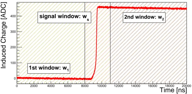
As mentioned in Sec. 5, the DAQ features a sampling rate of 250 MHz, which corresponds to a sample interval of 4 ns. In case of a trigger, a 20 µs window with a fixed number of samples before and after the trigger is opened. This way, all pulses start at the same position. This is necessary for the fixed window method. Since the charge collection time and consequently the pulse rise-time varies from event to event, the signal window, w
shas to be su ffi ciently large to make sure the pulse starts and reaches its maximum inside the signal window. Experience shows, that for the given detector geometry and operational characteristics, the rise-time is always shorter than 3 µs. This corresponds to 750 samples. The total number of samples is 5000. Window one, w
1, was defined to contain the samples 0 to 2000 and window two, w
2, the samples from 2750 to 4999. The samples within w
1and w
2were averaged. The amplitude of the pulse, M, is calculated as the di ff erence of the averaged values and is in units of ADC counts.
Time [ns]
0 2000 4000 6000 8000 10000 12000 14000 16000 18000 20000
Induced Charge [ADC]
0 100 200 300 400
1st window: w
12nd window: w
2signal window: w
sFigure 6.2.: The example pulse introduced in the previous chapter. The fixed windows used for the amplitude determination of the measured pulses are indicated.
6.2.2. Sliding Window Method
As an alternative to the fixed window method, the sliding window method was tested in vari-
6. Signal Processing
which is also used by the DAQ. It is also called trapezoidal filter. For this procedure, it is not necessary to know the time at which the pulse starts. Two so called rise-time windows, rt, slide over the total time range. They are separated by a fixed number of samples called the flat-top, f t. The windows slide by one sample at a time. This is referred to as a step. For each step, the pulse-heights within the rt windows are averaged. The di ff erence between the averages is entered in a histogram for step n. This results in a trapezoid with a flat top. The height of the trapezoid corresponds to the measured pulse amplitude, M. This method is based on the ampli- tude maximum. Thus, this method yields a non-zero energy for mirror pulses, even though no net charge is collected. However, when looking at single-segment events of known location, like the low energy
133Ba events, this method works very well. This is why it was also investigated as an option. For the sliding window filter, di ff erent configurations for the f t and rt windows were investigated. The used number of samples for the f t window is either 500 or 750, while the number of samples for the rt window varies respectively from 750 to 1500 in steps of 125.
6.2.3. Results
The photon peaks from the
133Ba source were fitted with a Gaussian after the application of the various filters. The histograms were roughly calibrated to match the photon peaks. The resolu- tion, E.Res, is shown as ratio of the fitted Full-Width-Half-Maximum, FW H M, and the fitted mean of the peak, Mean. The histograms are based on pulse amplitudes before cross-talk e ff ects were corrected, see next section. The uncertainties of the fit parameters are of the order of 1.5 % of the FW H Ms and of the order of 0.4 h of the Mean. This translates after propagation of the uncertainties, using ∆ E.Res/E.Res = p
( ∆ FW H M/FW H M)
2+ ( ∆ Mean/Mean)
2, to an uncer- tainty of the ratio, ∆ E.Res, of the order of 0.4 h [21]. Using the TS1 data set, Figures 6.3a and 6.3b show the results for the 81 keV peak as an example. Figures 6.4a and 6.4b show the results for both
60Co peaks, using the CO data. For consistency, only single-segment events were considered.
For low energies, the sliding window method yields a better core resolution by 0.002. For the segments, both methods yield similar results. In the case of segment 4, the fixed window method proves advantageous by 0.004. For segment 1, the fixed window method performs 0.004 worse. For segment 4, the resolution clearly improves for a higher number of samples in the rt windows. No substantial di ff erence is observed for the two settings for the f t window.
For higher energies, i.e. the 1173 keV and 1332 keV peaks of
60Co, the fits are more influenced by fluctuations. The trends observed for the barium lines only show for segment 4. This might be related to segment 4 having about 3 times more statistic. Noticeably, the core resolution for both sliding window and fixed window method are very similar for high energies.
As the sliding window method does not, in general, lead to better resolutions, the fixed win- dow method was chosen to determine the pulse amplitude. Due to the trigger configuration, the intrinsic advantage of the sliding window filter, where one does not need to know the start time of a pulse, is irrelevant. Thus, the advantages of the fixed window method concerning the treat- ment of mirror pulses can be exploited. The mirror pulses occur within the signal window, w
s, hence the di ff erence between the averaged w
2and w
1yields zero. In this case the fixed window method provides a robust and consistent treatment of any pulse.
28
6.2. Pulse Amplitude Determination
sl.w. ft500 rt750sl.w. ft500 rt875sl.w. ft500 rt1000sl.w. ft500 rt1125sl.w. ft500 rt1250sl.w. ft500 rt1375sl.w. ft500 rt1500sl.w. ft750 rt750sl.w. ft750 rt875sl.w. ft750 rt1000sl.w. ft750 rt1125sl.w. ft750 rt1250sl.w. ft750 rt1375sl.w. ft750 rt1500fixed window
E. Res. (FWHM / Mean)
0.018 0.02 0.022 0.024 0.026 0.028 0.03 0.032 0.034 0.036
Source facing seg. 1, March 9th Source facing seg. 2, March 10th
Source facing seg. 3, March 8th
Source facing seg. 4, March 10th
81 keV
(a) Source:
133Ba, collimated. The resolution for the sliding window method in di ff erent configurations and for the fixed window method. All values were obtained by Gaussian fits. All values correspond to the core read-out channel, the source was facing di ff erent segments.
sl.w. ft500 rt750sl.w. ft500 rt875sl.w. ft500 rt1000sl.w. ft500 rt1125sl.w. ft500 rt1250sl.w. ft500 rt1375sl.w. ft500 rt1500sl.w. ft750 rt750sl.w. ft750 rt875sl.w. ft750 rt1000sl.w. ft750 rt1125sl.w. ft750 rt1250sl.w. ft750 rt1375sl.w. ft750 rt1500fixed window
E. Res. (FWHM / Mean)
0.03 0.04 0.05 0.06 0.07 0.08 0.09 0.1
Seg. 1 Seg. 2 Seg. 3 Seg. 4
81 keV
(b) Source:
133Ba, collimated. The resolution for the sliding window method in di ff erent configurations and for the fixed window method. All values were obtained by Gaussian fits. Where the uncertainties are not visible, they are smaller than the symbol size.
This figure shows the segment resolutions for the data also analyzed for Fig. 6.3a. All
segments show similar dependencies on the sliding window filter configurations.
6. Signal Processing
sl.w. ft500 rt750sl.w. ft500 rt875sl.w. ft500 rt1000sl.w. ft500 rt1125sl.w. ft500 rt1250sl.w. ft500 rt1375sl.w. ft500 rt1500sl.w. ft750 rt750sl.w. ft750 rt875sl.w. ft750 rt1000sl.w. ft750 rt1125sl.w. ft750 rt1250sl.w. ft750 rt1375sl.w. ft750 rt1500fixed window
E. Res. (FWHM / Mean)
0.003 0.004 0.005 0.006 0.007 0.008 0.009
Core Seg. 1 Seg. 2 Seg. 3 Seg. 4
1173 keV
(a) Source:
60Co, uncollimated. The resolution for the sliding window method in di ff erent filter configurations and the fixed window method. Only single-segment events were used. All values were obtained by Gaussian fits.
sl.w. ft500 rt750sl.w. ft500 rt875sl.w. ft500 rt1000sl.w. ft500 rt1125sl.w. ft500 rt1250sl.w. ft500 rt1375sl.w. ft500 rt1500sl.w. ft750 rt750sl.w. ft750 rt875sl.w. ft750 rt1000sl.w. ft750 rt1125sl.w. ft750 rt1250sl.w. ft750 rt1375sl.w. ft750 rt1500fixed window
E. Res. (FWHM / Mean)
0.002 0.003 0.004 0.005 0.006 0.007 0.008
Core Seg. 1 Seg. 2 Seg. 3 Seg. 4
1332 keV
(b) Source:
60Co, uncollimated. The resolution for the sliding window method in di ff erent filter configurations and the fixed window method. Only single-segment events were used. All values were obtained by Gaussian fits.
Figure 6.4.
30
6.3. Reconstructing the Deposited Energy
6.3. Reconstructing the Deposited Energy
In any segmented detector, cross-talk has to be considered before the amplitudes can be con- verted to energies. Two kinds of cross-talk e ff ects occur in segmented semiconductor detectors:
• Intrinsic Cross-talk: Due to the capacitance between detector segments.
• Electronic Cross-talk: Due to the capacitance between cables and other elements of the read-out circuit.
In this thesis, intrinsic and electronic cross-talk are treated together. In addition to cross-talk, the individual amplification factors of di ff erent preamplifiers have to be taken into account.
In order to reconstruct the true Energy, E
itrue, where i ∈ [0,1,2,3,4], for each channel, all the influences on E
trueleading to the measured pulse amplitudes, M
i, have to be corrected for.
The index 0 refers to the core and i = 1, 2, 3, 4 refers to the segments, see Sec. 4. Cross-talk and amplification happen at di ff erent stages during the pulse read-out. Both are assumed to be linear.
Before all other e ff ects, intrinsic cross-talk occurs on detector level due to the capacitances between the segments. As a result, the energies observed in the segments change. It can be expressed via an intrinsic cross-talk matrix, c
ini j, j ∈ [0,1,2,3,4]. The resulting values correspond to the true energies after the influence of intrinsic cross-talk, E
ini:
E
true0. . . E
true4·
1 c
in01. . . c
in04c
in10... ... ...
... ... ... ...
c
in40. . . . 1
=
E
in0. . . E
4in. (6.1)
The indices i, j are read as cross-talk from channel i to channel j. By definition, the cross-talk from any segment to itself is 1. The core channel exclusively gets partially amplified close to the detector, since its JFET is installed right in the cryostat, see Sec. 5. This can be expressed via a diagonal matrix, f
i j:
E
in0. . . E
in4·
f
00 . . . 0 0 1 ... ...
... ... ... ...
0 . . . . 1
=
f
0· E
in0E
in1. . . E
4in. (6.2)
Before the signals reach the preamplifiers the electric transfer cross-talk occurs. The respective matrix, c
eti j, leads to values E
ic. Again, the c
etiiare 1 by definition:
f
0· E
in0E
1in. . . E
in4·
1 c
et01. . . c
et04c
et10... ... ...
... ... ... ...
=
E
0c. . . E
c4. (6.3)
6. Signal Processing
The E
ciare subject to the amplification in the respective preamplifiers. At this point it is assumed that no further cross-talk occurs. The corresponding matrix, a
i j, finally leads to the measured ADC counts, M
i:
E
0c. . . E
4c·
a
F00 . . . 0 0 a
1... ...
... ... ... ...
0 . . . . a
4
=
M
0. . . M
4. (6.4)
The above matrices can be multiplied, resulting in one matrix, c
∗i j, which now links E
itrueand M
i:
E
0true. . . E
true4·
c
∗00. . . c
∗04... ... ...
c
∗40. . . c
∗44
=
M
0. . . M
4. (6.5)
The true energies, E
itruecan be determined using the inverse matrix c
∗i j−1:
E
true0. . . E
true4=
M
0. . . M
4·
c
∗00. . . c
∗04... ... ...
c
∗40. . . c
∗44
−1
. (6.6)
The assumption of linearity persists through the above considerations. No E
2term or terms of even higher order are introduced.
6.3.1. Procedure for cross-talk correction and energy calibration
The determination of the values of all c
∗i jproves di ffi cult, since there are too few equations based on only the M
ivalues. The matrix can be reduced by one dimension from 5 × 5 to 4 × 4 by the following considerations. The measured pulse amplitude for the core, M
0, can be written as:
M
0= E
true0· c
∗00+ E
true1· c
∗10+ . . . + E
true4· c
∗40. (6.7) By introducing the assumption that the cross-talk from the segments to the core is the same for all the segments, c
∗10= c
∗i0, i ∈ { 2, 3, 4 } and using the identity P
4i=1
E
truei= E
0true, M
0becomes:
M
0= E
0true· (c
∗00+ c
∗10) (6.8)
= E
0true· c
core. (6.9)
The value of the thus defined c
corecan be determined by the standard procedure of fitting the core spectrum with the known photon lines using all events.
It is impossible to separate the cross-talk to one specific segment into the part originating
from the core and the part originating from the other segments, since the core always sees the
full energy and influences all segments. Thus, the cross-talk from the core to the segments
can mathematically be unified with the segment to segment cross-talk. For demonstration,
32
6.3. Reconstructing the Deposited Energy
consider the measured pulse amplitude for segment 1, M
1. Again making use of the identity P
4i=1
E
itrue= E
0true:
M
1= X
4i=0
E
truei· c
∗i1(6.10)
= E
0true· c
∗01+ X
4i=1
E
itrue· c
∗i1(6.11)
=
4
X
i=1
E
truei· c
∗01+
4
X
i=1
E
truei· c
∗i1(6.12)
=
4
X
i=1
E
truei(c
∗01+ c
∗i1) =
4
X
i=1
E
itrue· c
i1. (6.13) The application of the above equations to all the segments, respectively, results in the reduced matrix c
i j, i, j ∈ { 1, 2, 3, 4 } and the equations:
M
0= E
0true· c
core(6.14)
M
1. . . M
4=
E
true1. . . E
true4·
c
11. . . c
14... ... ...
c
41. . . c
44
. (6.15)
The matrix elements c
i jcan be determined by investigating single-segment events. In a single- segment 1 event, for example, all the energy is deposited in only segment 1. Thus, the true energy of this segment equals the true energy of the core, E
1true= E
0true, and the energy deposited in the remaining segments equals zero, E
2true= E
3true= E
true4= 0. In general, for single-segment i events, E
itrue= E
true0, E
truej,i
= 0. Single-segment events are selected by analyzing the distribution of ratios between the pulse amplitude of the respective segment and the pulse amplitude of the core, R
ssi= M
i/M
0. Figure 6.5a shows the corresponding histograms. Events in the peak around ≈ 0.75 correspond to the single-segment events. The mean of the peak corresponds to R
ssi. Using segment 1 as an example, the measured pulse amplitude for single-segment 1 events, M
1, can then be written as:
M
1= E
true1· c
11+ E
2true· c
21+ E
3true· c
31+ E
true4· c
41(6.16)
= E
true1· c
11+ 0 · c
21. . . (6.17)
In general, for single-segment i events, M
i= E
i· c
ii, i ∈ {1, 2, 3, 4}. Then, with Eq. 6.14, the matrix elements c
iican be determined:
c
ii= M
iE
itrue= M
iE
0true= M
i· c
coreM
0(6.18)
= R
ssi· c
core. (6.19)
The remaining matrix elements can also be determined studying single-segment events. For
single-segment i events, the measured pulse amplitudes in the other segments j, j , i, can be
written as:
6. Signal Processing
and the ratio between M
jand M
i, m
ji= M
j/M
i, leads to:
m
ji= E
truei· c
i jE
truei· c
ii= c
i jc
ii(6.21)
⇒ c
i j= m
ji· c
ii. (6.22)
The c
iivalues are already known from Eq. 6.18 and the m
jivalues can be determined by fitting the peak of the M
j/M
iratio. Figure 6.6 shows the corresponding histograms for selected single- segment 1 events. A typical matrix c is:
c =
0.2670 − 0.0007 − 0.0008 0.0015
−0.0007 0.2645 −0.0007 0.0036
−0.0007 −0.0006 0.2732 0.0013 0.0030 0.0030 0.0030 0.2668
, (6.23)
which can be inverted:
c
−1=
3.7450 0.0095 0.0112 − 0.0209 0.0106 3.7813 0.0106 −0.0517 0.0095 0.0082 3.6602 −0.0175
− 0.0419 − 0.0425 − 0.0414 3.7491
. (6.24)
The estimates for the energies deposited in each channel, E
chn, with chn ∈ {0, 1, 2, 3, 4}, are now calculated as:
E
0= M
0c
core(6.25)
E
1. . . E
4=
M
1. . . M
4· c
−1. (6.26)
34
6.3. Reconstructing the Deposited Energy
/ M0
M1
0 0.2 0.4 0.6 0.8 1
Events
1 10 102 103
/ M0
M2
0 0.2 0.4 0.6 0.8 1
Events
1 10 102 103
/ M0
M3
0 0.2 0.4 0.6 0.8 1
Events
1 10 102 103
/ M0
M4
0 0.2 0.4 0.6 0.8 1
Events
1 10 102 103
(a) Since the pulse amplitudes are not yet calibrated, the peak formed by single-segment events is not at M
i/M
0= 1 but rather around 0.75. The double structure on the peak near zero occurs due to cross-talk of the segments among each other. The minor peaks at 1.0 correspond to saturation events.
/ M0
M1
0.65 0.7 0.75 0.8 0.85 0.9
Events
1 10 102 103
Mean: 0.7768 : 0.00493 σ
/ M0
M2
0.65 0.7 0.75 0.8 0.85 0.9
Events
1 10 102
103 Mean: 0.7564
: 0.00383 σ
/ M0
M3
0.65 0.7 0.75 0.8 0.85 0.9
Events
1 10 102
103 Mean: 0.7802
: 0.00435 σ
/ M0
M4
0.65 0.7 0.75 0.8 0.85 0.9
Events
10 102
103 Mean: 0.7831
: 0.00430 σ