Atomic Force Microscopy in the Picometer Regime - Resolving Spins and Non-Trivial Surface Terminations
Florian Pielmeier 2014
Atomic Force Microscopy in the Picometer Regime - Resolving Spins and Non-Trivial
Surface Terminations
Dissertation zur Erlangung des Doktorgrades der Naturwissenschaften (Dr. rer. nat.) der Fakultät für Physik
der Universität Regensburg
vorgelegt von Florian Pielmeier
aus Regensburg
im Jahr 2014
Die Arbeit wurde von Prof. Dr. Franz J. Gießibl angeleitet.
Das Promotionsgesuch wurde am 16. April 2014 eingereicht.
Das Promotionskolloquium fand am 19. September 2014 statt.
Prüfungsausschuss: Vorsitzender: PD Dr. Falk Bruckmann 1. Gutachter: Prof. Dr. Franz J. Gießibl 2. Gutachter: Prof. Dr. Christian Back weiterer Prüfer: Prof. Dr. Christian Schüller
Contents
1. Introduction 1
2. Fundamentals of Scanning Probe Microscopy 5
2.1. Scanning Tunneling Microscopy (STM) . . . 5
2.2. Atomic Force Microscopy (AFM) . . . 7
2.2.1. Long-Range Forces between Tip and Sample . . . 7
2.2.2. Short-Range Forces between Tip and Sample . . . 9
2.2.3. Frequency Modulation Atomic Force Microscopy . . . 11
3. Comparison of Quartz-Based Force Sensors 17 3.1. Operating Principle and Theoretical Sensitivity . . . 18
3.2. Measurement of the Sensitivity of Quartz-Based Force Sensors . . . . 22
3.3. Noise Contributions in FM-AFM . . . 30
3.3.1. Deflection Detector Noise . . . 30
3.3.2. Thermal Noise . . . 32
3.3.3. Oscillator Noise . . . 33
3.3.4. Thermal Frequency Drift Noise . . . 33
3.3.5. Noise at the Frequency Demodulator Output . . . 35
3.4. Optimization of Quartz-Based Force Sensors . . . 38
3.4.1. Decreasing Deflection Detector Noise . . . 38
3.4.2. Decreasing Thermal, Oscillator, and Thermal Frequency Drift Noise . . . 43
3.4.3. Comparison of Noise Contributions for Optimized Sensors . . 44
3.5. Characterization of Quartz Resonators at Cryogenic Temperatures . . 46
4. Experimental Tools and Setup 53 4.1. Low Temperature STM/AFM Setup . . . 53
4.1.1. Omicron qPlus Sensor . . . 54
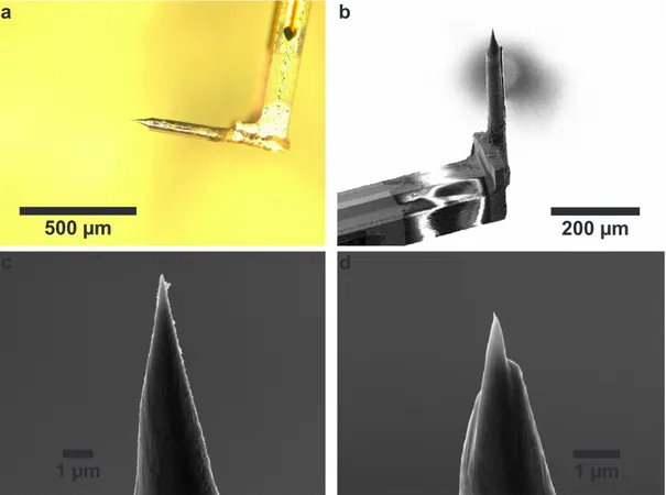
4.2. Fabrication of Magnetic Tips . . . 56
4.2.1. Electrochemically Etched Iron Tips . . . 56
i
Contents
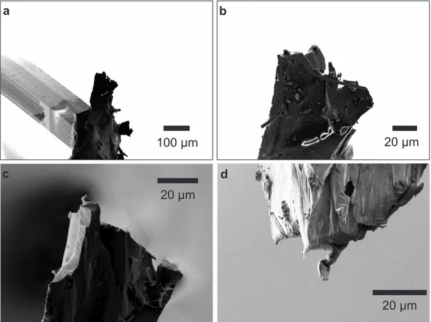
4.2.2. Bulk Samarium-Cobalt Tips . . . 59
5. Angular Dependent Short-Range Forces 61 5.1. Introduction to AFM with Subatomic Resolution . . . 61
5.2. Experimental Methods and Data Analysis . . . 64
5.3. Adatoms Studied with CO Functionalized Tips . . . 69
5.3.1. Cu Adatoms on Cu(111) . . . 69
5.3.2. Cu Adatoms on Cu(110) . . . 72
5.3.3. Model for the Charge Density of a Cu Adatom on Cu(110) . . 81
5.3.4. Discussion . . . 84
5.4. Characterization of Bulk Iron Tips . . . 87
6. Spin Resolution and Evidence for Superexchange on NiO(001) Observed by Force Microscopy 93 6.1. Introduction to Spin-Resolved Force Microscopy . . . 93
6.2. Measurements with Iron Tips . . . 97
6.2.1. Results with Uncharacterized Iron Tips . . . 97
6.2.2. Results with Characterized Iron Tips . . . 101
6.3. Measurements and Results with Samarium-Cobalt Tips . . . 104
6.4. Discussion . . . 108
7. Determination of TlBiSe2 Surface Termination by Force Microscopy 111 7.1. Introduction to Topological Insulators . . . 111
7.2. Properties of TlBiSe2 and Results of STM/AFM Measurements . . . 113
7.3. Discussion . . . 123
8. Summary 125 A. Appendix 129 A.1. Non-Standard qPlus Sensors . . . 129
A.1.1. Stiffness of Optimized qPlus Sensors . . . 129
A.1.2. Thermal Peaks of Non-Standard qPlus Sensors . . . 134
A.2. Charge Density Model: Determination of the Screening Constant . . 135
A.3. TlBiSe2: Determination of the Surface Coverage . . . 136
Bibliography 137
Acknowledgment 161
ii
1. Introduction
The discovery of the giant magnetoresistance effect in 1988 [1, 2] led to the first technologically relevant electronic devices utilizing not only the charge, but also the spin degree of freedom of an electron [3]. In the meantime, the field of spin-based electronics (spintronics) was growing rapidly, in particular in the area of data storage devices [4]. This also led to the development and investigation of a large number of materials from diluted magnetic semiconductors to topologically insulating materials [5]. With shrinking device size – Intel presented the first processor based on 14 nm technology last year [6] – the investigation of structural and magnetic properties at the atomic scale becomes more and more important.
The scanning tunneling microscope (STM) [7] as well as the atomic force microso- cope (AFM) [8] allow real-space imaging at the atomic scale [9, 10]. Spin-polarized STM (SP-STM) [11] and magnetic force microscopy (MFM) [12] enabled the investi- gation of magnetic structures at the nanoscale already around 1990. Ten years later antiferromagnetic structures were imaged at the atomic scale with SP-STM [13], and in 2007 the antiferromagnetic structure of a transition metal oxide was resolved by AFM utilizing iron coated silicon cantilevers [14]. In both experiments, the measured atomic corrugations were quite small, 3−4 pm and 0.5−1.5 pm, respectively. The detection of such tiny signals necessitates experimental setups with very low noise, which is achieved by operating the microscopes at cryogenic temperatures.
The development of the qPlus sensor offered the possibility to perform STM and AFM simultaneously, which made it a versatile tool in the field of scanning probe microscopy [15, 16]. This sensor is based on standard quartz tuning forks used in clocks and wrist watches. Its larger stiffness compared to standard silicon cantilevers allows stable operation at sub-Angstrom oscillation amplitudes, leading to an increased sensitivity for short-range interaction forces [17]. Although excellent results were obtained with qPlus force sensors, like subatomic resolution [18–20], submolecular resolution [21], and the detection of single charges on individual atoms [22], the resolution of magnetic structures at the atomic scale still remains a challenge [23].
In this thesis, the relevant figures of merit determining the signal-to-noise ratio
1
1. Introduction
(SNR) of quartz-based force sensors are analyzed, suggesting an improved SNR for miniaturized sensors. Modified qPlus force sensors are characterized at room and cryogenic temperatures and the expected improvement in SNR is confirmed.
These modified sensors are then used to resolve the antiferromagnetic structure of the nickel oxide (NiO) (001) surface. NiO is a prototypical antiferromagnetic insulator with planes of oppositely aligned Ni spins along the [111] direction. Apart from imaging the different spin states of the Ni ions at the surface, the spin state of sub-surface Ni ions was also detected due to a superexchange mechanism between tip and sample.
The exchange interactions between tip and sample are also studied quantitatively where the magnitude of the measured exchange force is an order of magnitude smaller than predicted theoretically [24, 25]. The strength of the spin-related signal depends crucially on the tip material and best results were obtained with a tip made of a samarium cobalt alloy, a magnetically hard material.
A new class of materials, topological insulators (TI), have attracted a lot of attention in recent years due to their unique electrical properties [26]. Spin-orbit interaction leads to the formation of a helical surface state, where the propagation direction of electrons is coupled to their spin state. In absence of magnetic impurities which break time reversal symmetry the backscattering between different spin states is suppressed [27]. Usual TIs have bulk band gaps of a few tens to hundreds of meV and often the surface states mix with bulk states [5]. These materials are often layered ternary systems and for band structure determination with angle-resolved photoemission spectroscopy (ARPES) they are cleaved in-situ, though it is not a priori obvious where the cleaving occurs. Here, we study the surface of cleaved TlBiSe2, a promising candidate for room temperature applications due to its relatively large band gap of around 250 meV. In STM mode, hexagonally ordered, nanometer sized patches could be identified. The AFM data additionally revealed a hexagonal atomic structure within these patches. From a detailed analysis of step heights and atomically resolved data, we deduce that the surface layer is formed by Tl islands. The disrupted surface layer explains the absence of trivial surface states in ARPES experiments [28].
This thesis is outlined as follows. In chapter 2 the basic theory and operating principle of STM and AFM is introduced. In particular, frequency modulation AFM (FM-AFM) [29] which is the operation mode used throughout this work.
The third chapter starts with a detailed introduction to quartz-based force sensors, followed by an experimental and theoretical comparison of the SNR of force sensors utilizing different quartz resonator geometries, namely tuning forks and length exten- sional resonators. As mentioned above, the relevant figures of merit are evaluated for
2
various types of sensors, clearly favoring miniaturized qPlus sensors in terms of SNR.
Finally, the frequency change with temperature for a number of quartz resonators is determined at cryogenic temperatures.
The experimental setup, a combined STM/AFM ultrahigh vacuum system operated at liquid helium temperatures, is described in chapter 4. Furthermore, the tip preparation procedures used to fabricate magnetic tips are explained.
Chapter 5 deals with investigation of individual copper (Cu) adatoms on the (110) and (111) facets of a Cu single crystal with carbon monoxide (CO) functionalized tips. The measurements on Cu/Cu(110) revealed for the first time a non-trivial subatomic structure within a single atom on a flat surface. The comparison of the adatom data with complementary experiments, where a bulk Cu tip is probed by a CO molecule adsorbed on Cu(111), suggests a different interpretation of previously obtained “subatomically” resolved data [20, 30].
In chapter 6 spin-resolved measurements of the NiO(001) surface, as outlined above, are presented. Experiments with two different tip materials, bulk iron tips and SmCo tips, were conducted.
The surface termination of TlBiSe2 is investigated in chapter 7, by a combination of STM and AFM imaging. The results suggest a disruption of the surface layer upon sample cleaving leading to a, at first glance, irregular surface structure.
3
2. Fundamentals of Scanning Probe Microscopy
This chapter briefly recaps the basic theory and operating principle of scanning tunneling microscopy in section 2.1. The focus of this work is mainly on atomic force microscopy, therefore this technique is described in more detail in section 2.2.
2.1. Scanning Tunneling Microscopy (STM)
Scanning tunneling microscopy was introduced by Binnig et al. in 1982 [7]. The capability of real-space atomic imaging and highly local spectroscopy was a major breakthrough in surface science [9,31]. In STM piezoelectric elements (piezos) position a sharp metal tip laterally (x, y-direction) and vertically (z-direction) over a conductive sample. If a bias voltage V is applied between the two electrodes, a current flows between tip and sample already before an ohmic contact is formed. This current originates from quantum mechanical tunneling of electrons through the vacuum gap or more general the potential barrier between tip and sample [32, 33]. A simple model that reproduces the key observables is a rectangular potential barrier, where the barrier height is approximately given by the average value of tip (ΦT) and sample (ΦS) work functions Φ = (ΦT + ΦS)/2 [33, 34]. From a quantum mechanical treatment of this one-dimensional potential wall the distance dependence of the tunneling current follows as [33]:
I(z) = I0exp(−2κz), (2.1)
where κ = √
2meΦ/~ with free electron mass me and reduced Planck constant ~. Common electrode materials are W and Cu with work function values of Φ≈4.6 eV [35] and a resulting value of κ≈11 nm−1. Roughly, the tunneling current changes by an order of magnitude when the tip-sample distance changes by 100 pm. Furthermore, I(z) is a monotonic function, enabling a straightforward implementation of a feedback circuit to control the tip-sample distance (constant current mode) by adjusting the z-position of the tip with the piezos. Another operation mode of the STM is the
5
2. Fundamentals of Scanning Probe Microscopy
constant height mode, where the feedback is switched off and the tip position in z-direction remains unchanged. In this mode a flat sample surface and a high stability of the microscope are mandatory.
In this work, the tunneling current is often used to determine the tip-sample distance with respect to a metal-metal point contact, whose conductance is given by the single- channel, spin-degenerate quantum of conductanceG0 = 2e2/h= (12906 Ω)−1, where e is the elementary charge andhis Planck’s constant [34, 36]. The junction conductance G(z) =I(z)/V =G0exp(−2κz) follows from Eq. (2.1). If the tip is oscillating with amplitude A at a frequency f like in a combined STM/AFM setup, the measured conductance is usually1 a time average over one oscillation cycle and is given by
hG(z)i=G0exp(−2κz)I0(2κA) exp(−2κA), (2.2) where I0(2κA) is the modified Bessel function of the first kind [16, 34]. For typical values ofκ= 11 nm−1 andA= 50 pm, I0(2κA) = 1.33 and I0(2κA) exp(−2κA) = 0.44.
Hence, the average conductance at A = 50 pm is only about half the value of the stationary case. For an accurate determination of z it is therefore important to take the averaging into account. If κ is known from hG(z)i or rather hI(z)i curves Eq.
(2.2) can be used to solve for z.
While equation Eq. (2.1) often leads to a correct description of current as a function of vertical tip height, it does not include a description of the electronic states or the influence of an applied bias voltage. Using Bardeen’s method one obtains in the limit of small temperatures the following expression for the tunneling current [33, 37]:
I(V) = 8π2 h
Z eV 0
ρT(EF −eV +)ρS(EF +)|M|2d. (2.3) Here,ρT ,S are the densities of states (DOS) of tip and sample, EF is the Fermi energy, and|M|2 is the tunneling matrix element which describes the probability of an electron tunneling from tip to sample or vice versa. In general, the STM measures a convolution of tip and sample DOS which makes a straightforward interpretation of STM data difficult. A common approximation is to assume spherical symmetric (s-wave) tip orbitals. Then the tunneling current is proportional to the local density of states of the sample at the Fermi energy, however, this holds only for small applied bias voltages (V Φ) [33, 38, 39]. The STM probes contours of constant local density of states in constant current mode and not the real topography of the sample.
1The bandwidth of the current preamplifier and of the input stage of the acquisition electronics is usually on the order of a few kHz whereasf >10 kHz.
6
2.2. Atomic Force Microscopy (AFM)
2.2. Atomic Force Microscopy (AFM)
The atomic force microscope (AFM) was developed, at least to some extent, to expand the STM capability of high resolution imaging to non-conductive samples [8]. A sharp tip is scanned again along a surface while the tip mounted to a cantilever, which gets deflected by tip-sample interaction forces. The key parameters of the cantilever are the spring constant k and, for dynamic operation modes, eigenfrequency f0 and quality factor Q. In the static mode, the deflection of the cantilever is directly proportional to the tip-sample forces. Obviously, this is problematic because a high force sensitivity is accompanied with a small restoring force which can lead to tip-sample collisions.
This problem is solved by oscillating the cantilever at an amplitude A in the so-called dynamic mode [16]. Either amplitude modulation (AM) [40] or frequency modulation (FM) [29] is used to detect tip-sample interactions. In AM-AFM, the cantilever is excited with a constant amplitude at a fixed frequency and changes in amplitude and phase of the oscillating cantilever upon tip-sample interactions are monitored. These changes occur on a time scale directly proportional to the Q value [16]. In ultra-high vacuum (UHV) and especially at low temperatures Q values exceeding 106 can be achieved, leading to a significant reduction in acquisition speed in AM mode. The FM-AFM mode, which is solely used throughout this work, overcomes this limitation and furthermore enables quantitative force measurements which is challenging with AM-AFM [41]. Before discussing FM-AFM and quantitative force measurements in more detail, the various types of long- and short-range forces acting between tip and sample are outlined in the following.
2.2.1. Long-Range Forces between Tip and Sample
In AFM, forces which do not vary on the atomic scale are called long-range forces. In UHV the main contributions come from van der Waals and electrostatic interactions.
In general, the term van der Waals interaction describes dipole-dipole interactions where three cases can be distinguished. The interaction between permanent dipoles is referred to as orientation (Keesom) force, the interaction between a permanent and an induced dipole as induction (Debye) force, and the interaction between induced dipoles as dispersion (London) force [42, 43]. All these forces are attractive. For non-polar or weakly polar atoms and molecules the dispersion force constitutes the bulk part of the interaction between them [42]. In a semi-classical picture the dispersion force is caused by fluctuating charge distributions in an atom or molecule. They temporarily lead to an electric dipole inducing an oppositely oriented dipole which causes attraction between the two objects. In quantum mechanics the dispersion force follows from
7
2. Fundamentals of Scanning Probe Microscopy
second-order perturbation theory [42–44]. Throughout this thesis the term van der Waals (vdW) refers to the dispersion force, as these are the main contributions to the tip-sample interaction in AFM. The distance dependence of the vdW interaction potential between two atoms is given by
UvdW =−C
z6, (2.4)
where z is the distance between the atoms and C the London-van der Waals constant.
Besides this short-range contribution to the tip-sample interaction, there is actually a much larger contribution due to the vdW interaction between macroscopic objects.
This can be calculated by pairwise summation over all particles or integration over the geometric structure [43, 45]. For a parabolic tip with local radius R and a flat sample, the vdW force is given as follows [43]:
FvdW=−AHR
6z2 . (2.5)
Here, AH is the Hamaker constant, which is around 1 eV for most solids [16]. The above equation describes no longer a short-range interaction, but a long-range force contribution which adds as an attractive background force to the tip-sample interaction.
The distance dependence of the vdW force between tip and sample generally follows a z−n power law, wheren is usually between 1 and 2 [45]. In an AFM setup, given that the sample is flat, the resulting vdW forces depend on the tip geometry, and sharp tips reduce the influence of these long-range contributions. Electrostatic interactions arise between a conductive tip and sample due to differences in the contact potential, giving rise to a capacitanceC(z) between them. If a bias voltage V is applied, the force can be described as follows:
Fel = 1 2
∂C
∂z (V −VCPD)2, (2.6)
with VCPD as contact potential difference (CPD). Fel is minimized when the applied bias voltage V compensates the CPD. Note, this picture still holds on insulating samples. In this case, the capacitor is filled with a dielectric media and the electric polarization on the sample surface is measured. One usually obtains again a parabolic dependence of the tip-sample interaction on the bias voltageV [46].
Another type of long-range force contribution is due to magnetic dipole-dipole interactions. These are used in Magnetic Force Microscopy (MFM) to study domain structured samples with a magnetized tip [12, 47]. The resolution is on the order of
8
2.2. Atomic Force Microscopy (AFM)
10 nm [48, 49]. The magnetic force acting between tip and sample is given as
Fmag =µ0(m∇)H, (2.7)
mis the magnetic moment of the tip andHthe sample magnetization. This interaction is quite weak and predominated by electrostatic and vdW forces. The contribution is negligible if either tip or sample is antiferromagnetic [39].
2.2.2. Short-Range Forces between Tip and Sample
Short-range forces are chemical bonding forces between the foremost atoms in tip and sample and give rise to atomic resolution imaging with AFM. Chemical bonds in solids include vdW bonds, ionic bonds, covalent bonds, and metallic bonds. These will be briefly discussed in the following. As mentioned above, the vdW interaction between single particles is short-range in nature (Eq. (2.4)), but usually negligible compared to other chemical bonding forces. Nevertheless, on inert samples like noble gas solids they allow atomic resolution imaging [50]. The total interaction is not solely attractive. To account for the repulsion of the electron clouds at close distances due to the Pauli exclusion principle [51] an empirical repulsive 1/zn term is added to the vdW potential. For n = 12 one obtains the well-known form of the Lennard-Jones Potential [52]:
ULJ =U0
"σ0 z
12
−2
σ0 z
6#
, (2.8)
where U0 is the bonding energy at the equilibrium distance σ0.
In ionic crystals the bonding is described by electrostatic attraction between pos- itively charged cations and negatively charged anions. To obtain an equilibrium bonding length an empirical repulsion term is added to the Coulomb potential [53,54].
If one sums the electric field from all cation and anion sites on the surface of an ionic crystal the resulting electric field decays exponentially with distance [55]. The decay constant κ is given as κ = 2π/d, where d is the lattice constant of the surface unit cell; e.g. d=a0/√
2 for an ionic crystal with bulk rock salt structure [56]. For NaCl with a bulk lattice constant of 0.56 nm the decay constant is κ= 15.87 nm−1, which is even larger than typical values in STM. The strong exponential decay of the electric field is the reason why it is relatively easy to achieve atomic resolution imaging on ionic crystal surfaces with AFM [10, 57].
Ideally, vdW and ionic crystals can be described as closed shell systems, where no overlap between the wave functions of the particles occurs and the electrons are localized at the atomic sites. In metals electrons are delocalized and distributed
9
2. Fundamentals of Scanning Probe Microscopy
uniformly throughout the whole crystal leading to a reduction of their kinetic energy and the electrostatic repulsion between the ion cores is also reduced. This picture only holds for simple metals like Li, Na, or Ka. The remaining core electrons form again a closed shell system [53]. In between ionic and metallic bonding character is covalent bonding, where the individual atomic orbitals overlap and form new orbitals, bonding and anti bonding ones. The standard example is the H+2 molecule. The increased electron density between the H+ ions reduces electrostatic repulsion. Such a simple system can be described to a good approximation by the semi-empirical Morse potential [58]
UM =−U0
2 exp
−z−σ0 λ
−exp
−2z−σ0 λ
, (2.9)
where U0 is the bonding energy andσ0 the equilibrium distance. The decay lengths λ andλ/2 correspond to the attractive and repulsive part of the interaction. Similar to the Lennard-Jones potential the repulsive part is added empirically and originates from the Pauli repulsion at close distances.
The chemical bonding forces described above determine structural and electronic properties of solids and enable atomic resolution imaging and site-dependent spec- troscopy with AFM. If one wants to study the magnetic structure of a sample on the atomic scale with AFM, the question arises which kind of short-range interaction between tip and sample can be employed to resolve the magnetic ordering. The classic dipole-dipole interaction between atomic magnetic moments is far too small to account for any magnetic ordering like ferro- or antiferromagnetism [53]. So far, there is no single model to explain all the various types of magnetic ordering in solids:
For example, the Heisenberg model [59] describes the interaction between localized spins well, but fails to explain ferromagnetism in itinerant electron systems like iron or cobalt [60]. Irrespective of the different characteristics of magnetic ordering they have a common origin: the so-called exchange interaction. It is a consequence of the Pauli exclusion principle for indistinguishable particles and the Coulomb interaction [51]. In general, if the spins align parallel the kinetic energy is increased and Coulomb energy is decreasing, whereas for antiparallel alignment the situation is reversed. In the simple case of a He atom in the ground state the two electrons align antiparallel, or more precise, they form a singlet state [61]. As a general consequence, the spin states influence the spatial part of the wave functions. This can of course also affect covalent bonding in solids, where a larger number of electrons is involved.
In force microscopy the interaction of the spins which are localized at the foremost tip and sample atoms is crucial and therefore the Heisenberg model is used to describe
10
2.2. Atomic Force Microscopy (AFM)
this situation [14, 39]. The Heisenberg model omits kinetic and Coulomb terms apart from the electron-electron interaction and solely considers the interaction between individual spins, leading to the following expression for the Hamiltonian:
Hspin=−X
ij
JijSi·Sj, (2.10)
the spin HamiltonianHspin depends on the relative alignment of the individual spins Si andSj, and only nearest-neighbor interaction is taken into account. The factor Jij is calledexchange integral or exchange coupling constant and is given as:
Jij =
Z Z
dridrjΨ∗i(ri)Ψ∗j(rj)HΨi(rj)Ψj(ri). (2.11) The Hamilton operator H =e2/|ri−rj|describes the pairwise Coulomb interaction and Ψ is the spatial part of the wave function of the particles. The name exchange integral is due to the exchange of coordinates between the corresponding Ψ and Ψ∗. If Jij is positive, ferromagnetic order is favored if Jij is negative, antiferromagnetic ordering is favored. AFM offers the unique ability to study exchange interaction between individual spins on the atomic scale. Therefore one has to combine the atomic resolution imaging capability of AFM with magnetic or rather spin-polarized tips [39]. The first experiment which unambiguously demonstrated the feasibility of this so-called Magnetic Exchange Force Microscopy (MExFM) was conducted in 2007 by Kaiser et al. [14]. Here, the antiferromagnetic order of the (001) surface of the insulator nickel oxide was resolved with atomic resolution. The term MExFM is somewhat misleading. Basically, the covalent bonds forming between tip and sample have different decay lengths depending on the extent of the wave functions which is determined by the different spin states.
2.2.3. Frequency Modulation Atomic Force Microscopy
In FM-AFM the force sensor, usually a single cantilever beam, is oscillated at constant amplitude A by an external drive signal [29]. The unperturbed cantilever can be described as a driven damped harmonic oscillator whose resonance frequency f0 is given as
f0 = 1 2π
s k
m∗, (2.12)
where k is the stiffness and m∗ = 0.24m is the effective mass of the oscillating beam [33]. A perturbation kts which acts on the cantilever oscillation can be included by
11
2. Fundamentals of Scanning Probe Microscopy
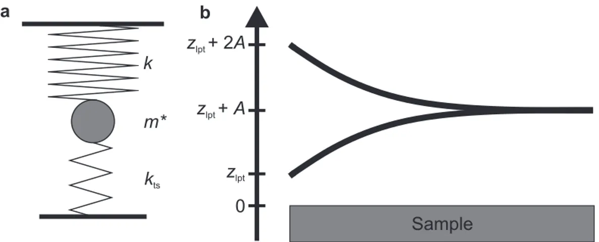
Sample b
0 zlpt
zlpt + A zlpt + 2A a
kts
m*
k
Figure 2.1.: Functional principle of AFM.a, equivalent mass and spring model for an oscillating beam with mass m∗ and stiffness k. The tip-sample interaction is modeled as an additional spring with stiffness kts. b, beam oscillating with amplitude A and definition of z-axis. The lower turnaround point of the oscillating beam is indicated withzlptand the base of the beam is then located at zlpt+A.
replacing the stiffnessk by an effective stiffness k∗ =k+kts (Fig. 2.1a). If the force gradient kts=−∂Fts/∂z is constant during one oscillation cycle of the cantilever and k kts, the square root in Eq. (2.12) can be expanded in a Taylor series and the change in resonance frequency ∆f =f −f0 to first order is
∆f(z) = f0
2kkts(z). (2.13)
The above gradient approximation is only justified if the oscillation amplitude A is significantly larger than the length scale of the interaction. For short-range forces one can assume an exponential force law with decay lengthλ and then, Aλ must be fulfilled to apply Eq. (2.13) [16]. In most experiments this condition is not met and the oscillation of the beam in the varying, non-linear tip-sample interaction potential Vts has to be taken into account.
The frequency shift ∆f is measured as a function of the vertical base position of the cantilever. When zlpt is the lower turnaround point of the oscillation then the base is at zlpt+A (Fig. 2.1b). Giessibl derived the following expression for the frequency shift ∆f [45]:
∆f(zlpt) = f0 2k
2 πA2
A Z
−A
Fts(zlpt+A+q0) q0
q
A2−q02
dq0. (2.14)
Here,Vts was treated as a small perturbation to the harmonic potential V =kA2/2 of the cantilever (Vts V). Equation (2.14) is valid for arbitrary amplitudes and
12
2.2. Atomic Force Microscopy (AFM)
describes a convolution of the force with an amplitude-dependent weight function.
Integrating Eq. (2.14) by parts results in a more intuitive expression:
∆f(zlpt) = f0 2k
2 πA2
A Z
−A
kts(zlpt+A+q0)qA2−q02dq0. (2.15)
Now, ∆f is given as a convolution of the force gradient kts and a weight function w(q0) = 2/(πA2)√
A2−q02 which describes a semicircle with radius A divided by its area πA2/2 [62]. Hence, one can still use the neat form of Eq. (2.13) by substituting the force gradientkts by an averaged force gradient
hkts(z)i=
A Z
−A
kts(z+A+q0)2qA2−q02
πA2 dq0. (2.16)
In FM-AFM forces are not directly measured. To recover Fts from measured ∆f(z) data Eq. (2.14) must be inverted. For this purpose several methods were proposed [63–66]. Most commonly used are the direct deconvolution methods by Giessibl [62]
and Sader and Jarvis [67]. In this work, forces are recovered by the Sader-Jarvis method and the implementation is based on a MATLAB script supplied by Welker et al. [68].
FM-AFM detects an averaged force gradient which offers the possibility to adjust the sensitivity to short- or long-range forces by a proper choice of the amplitude of oscillation A. For example, large amplitudes (∼10 nm) are required if one wants to detect magnetic stray fields and small amplitudes (∼0.1 nm) if one is interested in chemical bonding forces. On the other hand, for a stable oscillation of the cantilever (nojump-to-contact) it must be ensured that the restoring force of the cantilever is higher than the tip-sample forces. This leads to the following stability criterion [69]:
kA > Ftsmax. (2.17)
To detect large force gradients or respectively short-range forces it seems to be beneficial from Eq. (2.16) to use amplitudes as small as possible. On the other hand, noise also needs to be considered as it scales inversely with the amplitudeA [16, 29].
For exponentially decaying tip-sample forces with a decay lengthλ the optimal ratio between amplitude and decay length is A = 1.55λ [70]. In UHV the peak forces acting on the cantilever can be on the order of 100 nN [45]. This requires at least a stiffness of 1 kN when operating with amplitudes of A = 100 pm [69]. Throughout this work qPlus sensors with stiffness values exceeding k = 1800 N/m will be used
13
2. Fundamentals of Scanning Probe Microscopy
sample
cantilever deflection detection
φ A
reference f
PI-controller PI-controller excitation signal actuator
frequency shift Δf excitation
lock-in NCO
phase amplitude
AGC + PLL
Figure 2.2.: Block diagram of FM-AFM electronics. The colored box shows the basic components and signal paths of the automatic gain control (AGC) and phase-locked loop (PLL) as realized in the Nanonis OC4. The deflection signal of the cantilever is fed into a lock-in – excitation signal and frequency shift are then determined by seperate feedback loops and the numerical controlled oscillator (NCO), see text for more details.
[71,72]. Nevertheless, atomic resolution with FM-AFM on a reactive surface was first demonstrated with micro-fabricated Si-cantilevers with a stiffness ofk = 17 N/m and an amplitude ofA= 34 nm [73]. The signal-to-noise ratio needs to be analyzed in detail to judge which set of cantilever parameters (k, f0, Q) is optimal for atomic resolution imaging. A comparison of different types of force sensors and a discussion about the set of cantilever parameters (k, f0, Q) which is best suited for atomic resolution imaging based on a detailed analysis of the SNR in FM-AFM will be presented in chapter 3.
The basic operating principle of FM-AFM was introduced by Albrecht et al. [29].
The deflection signal from the cantilever is band-pass filtered and split up in two branches. One branch of the signal enters an amplitude controller consisting of an automatic gain controller (AGC) and a phase shift circuit to ensure positive feedback.
The second branch enters a frequency demodulator, which determines the resonance frequency of the oscillating cantilever. In the early days of FM-AFM the required electronics was purely analog. Later, a common combination was to use an analog amplitude controller and a commercially available digital phase-locked loop (PLL) [16]. Nowadays, state-of-the-art electronic circuits are purely digital. In this work a commercial oscillation control unit (Nanonis OC4)2 was used to keep A constant and to detect ∆f.
2OC4 - Nanonis Oscillation Controller, Specs Zurich GmbH, 8005 Zurich, Switzerland
14
2.2. Atomic Force Microscopy (AFM)
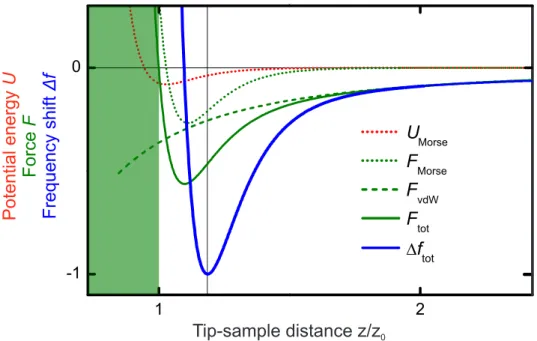
1 2
-1 0
UMorse
FMorse
FvdW
Ftot
ftot
Tip-sample distance z/z0
Potential energy U Force F Frequency shift Δf
Figure 2.3.:Short- and long-range contributions to the tip-sample interaction in AFM.
The short-range part is modeled by a Morse potential UMorse (dotted red) and the corresponding force is FMorse (dotted green). Adding a long-range vdW background forceFvdW (dashed green) to FMorse results in the total forceFtot (solid green). The corresponding frequency shift ∆ftot in the gradient approximation is shown in blue. In the green shaded regionFtot is repulsive, but often the region past the minimum in
∆ftot (vertical line) is called the “repulsive” interaction regime.
A block diagram is shown in Fig. 2.2. The deflection signal enters a lock-in which acts as a band-pass filter and detects amplitude A and phase ϕ of the deflection signal. Both are adjusted to their set point value by separate proportional and integral (PI) controllers. The phase signal is sent to a numerical controlled oscillator (NCO), which is triggered by an oven-controlled quartz oscillator (OCXO) with a stability of 1 ppb/day. The output signal of the NCO is the momentary oscillation frequencyf of the cantilever which is used again as a reference for the lock-in. After multiplication of the correction variable for the amplitude A with the momentary frequency f, the signal is routed to the actuator to excite the cantilever. The magnitude of this correction variable is a measure of the losses during an oscillation cycle. This is usually a combination of intrinsic losses of the excitation circuit including the sensor and dissipative processes between tip and sample [74]. The frequency shift ∆f =f −f0 is obtained by taking the difference between the momentary frequency f and the unperturbed resonance frequency f0;f0 must be determined in advance.
The frequency shift is caused by non-linear tip-sample interaction forces. Typical short- and long-range contributions are shown in Fig. 2.3. Short- and long-range forces are modeled as Morse and vdW forces (dotted and dashed green curves) and
15
their sum yields the total forceFtot (solid green curve) which determines the frequency shift ∆ftot (blue curve). Similar to the tunneling current in STM, ∆ftot can now be used as a feedback signal in an additional circuit to adjust the z-position of the cantilever. In contrast to the tunneling current, ∆f is not monotonic. In principle both slopes can be used for the feedback, but stable operation is only found in the regime where ∆ftot decreases with decreasing tip-sample distance z. This is called the “attractive” or non-contact regime. The region past the ∆f minimum is often called “repulsive” regime, although the total force is not yet repulsive there. The long-range attractive vdW background is not helpful to achieve atomic resolution imaging, but it is important for stable ∆f feedback operation. The long-range vdW interaction enables the tip to stay further away from the sample, when large-scale overview topography scans are desired. To achieve atomic resolution the ∆f setpoint is reduced to more negative values where the slope in ∆f(z) is larger. In the feedback or constant ∆f mode one cannot approach closer than the minimum in ∆f(z). To go even closer the constant height mode can be used.
For quantitative force determination, ∆f needs to be measured as a function of tip-sample distancez – a method called dynamic force spectroscopy [64]. By applying a bias voltageV to tip or sample, the local contact potential difference can be determined as at V =VCPD the electrostatic force Fel is minimized (see Eq. (2.6)) [75].
3. Comparison of Quartz-Based Force Sensors
Most of the work presented in this section has been published in Physical Review B1 [70] and Beilstein Journal of Nanotechnology2 [76]. Parts of the text are identical to the publications, in particular to the later one.
A number of impressive results including atomic resolution imaging [10, 55, 73], site dependent force spectroscopy [77], and atom manipulation at room temperature [78] were obtained by FM-AFM with standard silicon cantilevers with oscillation amplitudes in the nanometer range and stiffness values on the order of 10 N/m. On the other hand, the sensitivity to a given interaction increases when the amplitude A matches the length scale of the interaction [17, 70]. To study short-range forces it is therefore desirable to operate the force sensor with amplitudes on the order of 0.1 nm. Soft Si cantilevers cannot be operated at such small amplitudes, because they suffer from snap-to-contact [45]. It was suggested that stiffness values in the range of 300−3000 N/m are optimal for atomic resolution imaging [17]. Quartz tuning forks (TF) with a stiffness in the kN/m range were introduced by Güthneret al. in 1989 for distance control in scanning near field acoustic microscopy [79]. A major drawback of tuning forks is the coupled oscillation of the two prongs; any imbalance leads to a decrease in the quality factor Q [80]. Although the tip mass might be balanced by a counter weight [81], it is not possible to compensate the tip-sample interaction. For tuning forks this problem can be solved by immobilizing one of the two prongs to form a single harmonic oscillator where Qis not affected by the additional mass or tip-sample interactions. This configuration is called “qPlus” [71]. Another possibility is to use a coupled oscillator which has a significantly higher stiffness than
1F. J. Giessibl, F. Pielmeier, T. Eguchi, T. An and Y. Hasegawa,Comparison of force sensors for atomic force microscopy based on quartz tuning forks and length-extensional resonators,Physical Review B84, 125409 (2011).
2F. Pielmeier, D. Meuer, D. Schmid, C. Strunk, F. J. Giessibl,Impact of thermal frequency drift on highest precision force microscopy using quartz-based force sensors at low temperatures, Beilstein J.
Nanotechnology 5, 407 (2014).
17
3. Comparison of Quartz-Based Force Sensors
a standard tuning fork, e.g. a length extensional resonator with a stiffness far beyond 100 kN/m. In this case, the tip-sample interaction does not affect the oscillation very much and a high Q value can be retained. This configuration is called “needle”
sensor [82]. For obvious reasons it is challenging to detect the small influence of the tip-sample interaction on the oscillating prong. Nevertheless, atomic resolution in UHV on Si(111)-7×7 was obtained at room and low temperatures [83, 84]. In the following, the signal-to-noise ratio (SNR) of these two kinds of sensors is compared theoretically and experimentally.
3.1. Operating Principle and Theoretical Sensitivity
Before discussing the properties of quartz and the working principle of the sensors, an important difference between single and coupled oscillators needs to be pointed out. The standard formulas for FM-AFM (Eq. (2.13)-(2.16)) only hold for a single harmonic oscillator like the qPlus sensor and cannot be applied straightforward to coupled oscillators. The frequency shift ∆f of qPlus sensors is given as:
∆f = f0
2khktsi. (3.1)
For the LER the motion of both prongs relative to the support must be taken into account. The evaluation of a corresponding mechanical model showed that Eq. (3.1) still holds for coupled oscillators. Although, the effective stiffness k of a coupled oscillator is twice the value (kcoupled = 2k0) of a single oscillator (ksingle =k0) [70]. In other words, at a given interaction strength a coupled oscillator yields only half the frequency shift as a single oscillator. For the following discussion it is distinguished between geometrical stiffness k0 which is given by the beam dimensions and effective stiffnessk which must be used in Eq. (3.1). The k0 and k values for both sensors are summarized in Tab. 3.1.
Quartz resonators are used as frequency standards due to their small frequency varia- tion with temperature [85]. Quartz is crystalline SiO2 which appears in a lot of varieties in nature, whereas for device application synthetic α-quartz is commonly used [85].
For the following discussion quartz refers to α-quartz. This is the stable configuration of quartz at temperatures below 573◦C with a trigonal-trapezohedral crystal structure [86]. The standard convention of the axis assignment for right-handed synthetic quartz is shown in Fig. 3.1a. Thez-axis is parallel to the crystallographicc-direction and thex- axis is parallel to one of thea-directions [85,86]. Quartz is an anisotropic material. Its
18
3.1. Operating Principle and Theoretical Sensitivity
z
x
y y
z
x y
y
a b
φ
φ
z=c
x=a
y c
Figure 3.1.: Quartz crystal structure and orientation of crystal cuts. a, definition of rectangularx, y, z-axis system. Thez-axis coincides with the crystallographic c-axis,x with one of thea-axis, andy is chosen to be perpendicular toxandz. b,c, tuning forks and length extensional resonators are cut along thex, y0-plane. The angle ϕbetween y and y0 is typically in the range of 0−5◦. Figure partly adapted from [87].
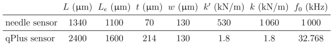
L (µm) Le (µm) t (µm) w (µm) k0 (kN/m) k (kN/m) f0 (kHz)
needle sensor 1340 1100 70 130 530 1 060 1 000
qPlus sensor 2400 1600 214 130 1.8 1.8 32.768
Table 3.1.: Geometrical parameters: lengthL, electrode length Le, thickness t, and widthw; geometrical stiffnessk0, effective stiffnessk, and eigenfrequencyf0of the quartz oscillators used.
properties, e.g. piezoelectric constants, elastic constants, and thermal expansion coeffi- cients, depend on the orientation relative to the crystal axes. Therefore, the frequency variation with temperature of quartz resonators can be tuned by choice of the orienta- tion of the crystal cut [85]. The standard crystal cut for TFs and LERs is depicted in Figs. 3.1b,c. The quartz crystal are cut almost along the orthogonalx, y, z-system, but there is a slight deviation along they-axis and the angleϕis usually between 0−5◦[87].
Thex, y, z-axes are also called electrical, mechanical, and optical axes, respectively [87].
The prongs of the TF oscillate parallel to the x-axis in a bending mode, whereas the prongs of the LER oscillate perpendicular to the x-axis in a length extensional mode.
A qPlus sensor is built by fixing one of the prongs of a TF to an electrically non- conductive substrate (Al2O3) with non-conductive glue3 (Fig. 3.2a). The LER is fixed to the substrate at its base without any modifications to form a needle sensor (Fig.
3.2b). Both resonators have two electrodes which are connected to the leads with conductive epoxy.4 A tip is mounted on the freely oscillating prongs. The standard
3J-B Weld, J-B Weld Company, Sulphur Springs, TX, USA.
4EPO-TEK T4110, EPOXY Technology, Billerica, MA, USA.
19
3. Comparison of Quartz-Based Force Sensors
a b c d e f g
h i j k l
x y t
L Le
A-A A-A
t w y
LLe
B-B B-B
t w
x
x σmech
σmech
z
Figure 3.2.: Geometry of qPlus and needle sensors. a, one prong of a quartz tuning fork is fixed to an insulating substrate with electrically non-conductive epoxy and the tip is attached to the free prong. b, the base of the LER is also fixed to a support.
A tiny tip is mounted on the non-encased prong. c,d,h,i, geometrical dimensions of qPlus and needle sensors as listed in Tab. 3.1. e,j, schematic view of the electrostatic field distribution in the cross section of each prong. f,k, mechanical stress profile along cross sections indicated in c andh. g,l, idealized field distribution within the quartz resonators. Figure adapted from [70].
geometries and electrode configurations of qPlus and needle sensors are outlined in Figs. 3.2c,d and Figs. 3.2h,i. The values for length L, thickness t, width w, and electrode length Le are summarized in Tab. 3.1.
Two important parameters of a force sensor in FM-AFM are the resonance frequency and the geometrical stiffness k0 of the oscillating beams. For the bending mode of the qPlus sensor the stiffnessk0 is given by [33]
k0 =k = Ewt3
4L3 , (3.2)
where E = 78.6 GPa is the Young modulus of quartz [88, 89]. The fundamental resonance frequencyf0 is given as [33]
f0 = 0.162 t
L2vs, (3.3)
where vs =qE/ρ andρ= 2650 kg/m3 are the velocity of sound and the mass density of quartz [88]. For the extensional mode of the needle sensor the stiffness k0 of each beam is given by
k0 = k
2 = Ewt
L (3.4)
and the resonance frequency is [70]
f0 = vs
4L. (3.5)
The charges generated by the quartz resonators are directly proportional to the
20
3.1. Operating Principle and Theoretical Sensitivity
deflection of the prongs. When the prong is bent or elongated strain is generated which leads to a mechanical stress σmech. The piezoelectric effect then causes the emergence of a surface charge density σel given by
σel =d12σmech, (3.6)
whered12= 2.31 pm/V [88] is the transverse piezoelectric coupling coefficient of quartz which is equal to the longitudinal coupling coefficient d11.5 It is important to note that d12 is almost constant from 1.5 K up to room temperature [88]. Integrating the surface charge density over the electrode area gives the total chargeqel generated by a given deflection with amplitudeA and the sensitivity is then defined as S =qel/A[70].
The above discussion assumes a homogeneous distribution of the electric field within the quartz crystal as depicted in Figs. 3.2g,l. Actually, the field distribution looks more like that drawn in Figs. 3.2e,j. Especially for the qPlus sensor the deviation is expected to be quite large. The dissimilar operation modes and the resulting difference in the strain profiles (Figs. 3.2f,k) results in different formulas for the theoretical sensitivity of qPlus and needle sensors. For a qPlus sensor the following expression was derived [18]:
SqPlustheo = 12d12k0Le(L−Le/2)
t2 . (3.7)
With the dimensions listed in Tab. 3.1 a standard qPlus sensor yields SqPlustheo = 2.79µC/m. The experimental sensitivity is expected to deviate from that value due to the non-ideal electric field distribution [70]. The influence of the electrode configuration was studied by Welker et al. [90, 91]. Here, a geometry factor g was introduced to account for this deviation. It was determined to g = 0.52 by measuring the deflection of the beam with an optical microscope in a stroboscope setup. This gives an actual sensitivity ofSqPlus = 1.46µC/m. Note, the error in the stroboscope setup is mainly determined by the accuracy of the optical deflection measurement which is estimated to about±5%.6
For the needle sensor the sensitivity is given by [70]
SLERtheo = 2d12k0L t sin
πLe 2L
. (3.8)
With the values from Tab. 3.1 the theoretical sensitivity of a needle sensor is determined
5Actually, d11=−d12 is negative for right-handed quartz [86], but because the prongs oscillate the sign of the generated charge changes periodically and is neglected for the following discussion.
6The measured deflections are in the order of 10µm and the optical resolution limit is around 0.5µm, resulting in a relative error of 5 %.
21
3. Comparison of Quartz-Based Force Sensors
to SLERtheo = 45.0µC/m. The experimental sensitivity is expected to be quite similar to the theoretical one as the deviation from the ideal field distribution is small for the needle geometry (Figs. 3.2j,l).
3.2. Measurement of the Sensitivity of Quartz-Based Force Sensors
The theoretical sensitivity defined above is the intrinsic sensitivity of the self-sensing quartz resonator which refers to charge generated per deflection by the piezoelectric effect. In AFM the term sensitivity generally refers to the output signal per deflection of the cantilever. This is independent from the measurement method and is usually given in units of V/m. In this sense, the sensitivity is the calibration factor for the oscillation amplitudeA. For the following discussion the intrinsic sensitivity is denoted asSC and the calibration factor as SV.
The oscillating beams generate a current which can be turned into a voltage output signal by a transimpedance amplifier or current-to-voltage converter (IVC, Fig. 3.3a).
To obtainSV the voltage output needs to be related to a given deflection. Therefore a reference amplitude is required. This can be achieved by measuring the output signal of the IVC without an external drive signal. Then the signal generated by the sensors due to random thermal excitation is measured. The equipartition theorem can then be employed to relate the voltage output signal to the thermally excited oscillation amplitude of the sensors. From there one can define the sensitivitySV [18].
The validity of this method was confirmed in a temperature range from 140−300 K for quartz tuning forks and can be applied to qPlus and needle sensors in a similar way [90]. To justify the application of the equipartition theorem the excitation of the quartz sensors must be purely thermal. Therefore any spurious excitation of the sensors must be avoided. Mechanical vibrations from the environment can be an issue, in particular ultrasonic sound can easily excite the sensors. The qPlus design is generally more prone to unwanted excitations than coupled oscillators. Vibrations of the base cause a symmetric oscillation of the prongs, but coupled resonators oscillate in an anti-symmetric mode. Another issue is spurious electrical excitation. This can happen in the following way: An increased input capacitanceCin almost inevitably leads to an increase of the electrical noise floor at the output of an electronic amplifier.
This is due to the input voltage noise density7 of the operational amplifier which, together with Cin, leads to an increase in charge or, respectively, current noise density
7For low noise amplifiers this is typically in the order of nV/√ Hz.
22
3.2. Measurement of the Sensitivity of Quartz-Based Force Sensors
C
ina
0.1 1 10 100 1000
1 10 100
gain G [mV/nA]
f [kHz]
IV converter charge amplifier +
C
fR
fshielding
sensor
V
outb
I
Figure 3.3.: Schematic setup to measure the thermal noise spectrum of a quartz sensor and transfer function of a current-to-voltage converter (IVC).a, the electrodes of the sensor are connected to ground and the IVC. Sensor and amplifier are placed in a grounded metal box for shielding. The output of the IVC is connected to a spectrum analyzer (not shown). b, ideal transfer function of an IVC with Rf = 100 MΩ and Cf = 0.1 pF (solid red line), the input capacitanceCin is not taken into account. For frequenciesf fc(here, fc= 16 kHz) the gain drops proportional to 1/f. The green shaded region marks the typical operating range of qPlus sensors which is beyond fc. The dashed black line corresponds to a constant charge gain of 1013V/C as realized by a commercial amplifier for a remarkably large frequency range from 250 Hz to 15 MHz.
at the input of the amplifier. The increased current noise density is transferred via the feedback resistance to a larger voltage noise at the output. If the amplifier is now connected to a self-sensing sensor there is another effect associated with this. The increased current noise at the input of the amplifier can serve as an electrical drive signal for the quartz resonator which might overwhelm the thermal white noise drive.
This can be avoided by directly connecting the sensor to the amplifier. Then Cin is mainly determined by the static capacitance of the quartz sensor which is about 1 pF for both types.8
From the equipartion theorem the magnitude of the thermal oscillation amplitude of a qPlus sensor follows as [18]
1
2khA2thi= 1
2kBT =⇒Armsth =qkBT /k. (3.9) With the definition of k = 2k0 for coupled oscillators Eq. (3.9) can also be used for tuning fork or needle sensors. At room temperature (T = 296 K) the thermal root mean square (rms) amplitude for a qPlus sensor is 1.5 pm and 62 fm for a needle
8Micro Crystal, DS-Series and CC4V-T1A data sheets for tuning forks and length extensional resonators, Micro Crystal, 2540 Grenchen, Switzerland.
23
3. Comparison of Quartz-Based Force Sensors
sensor. The experimental sensitivity is then defined as SV= Vthrms
Armsth , (3.10)
where Vthrms is the voltage output of the amplifier generated by thermal excitation of the quartz resonator. The thermal excitation signal is quite weak and it is not possible to measureVthrms directly with a voltage meter. One can instead measure the power spectral densityn2V of the amplifier output with a spectrum analyzer. The total power spectral densityn2V contains the power spectral density n2th, which is due to thermal excitation of the quartz resonator, and n2el, which is the electrical noise density of the amplifier. The output voltage Vthrms is therefore given via the following relation [90]:
(Vthrms)2 =
f0+B/2 Z
f0−B/2
n2th(f)df =
f0+B/2 Z
f0−B/2
n2V(f)−n2eldf. (3.11)
Here, the electrical noise densitynel is assumed to be constant within the measurement bandwidth B. This is justified for bandwidths of B ≈400−800 Hz which are usually used for the thermal peak measurements. The combination of Eqs. (3.9)-(3.11) allows to determine the sensitivitySV. This quantity depends on the amplifier and to relate SV toSC the charge gain in V/C needs to be determined from the transfer function of the amplifier.
The frequency response of an ideal IVC is given by Vout =− RfI
1 +i2πf RfCf, (3.12) where Rf is the feedback resistance and Cf its parasitic capacitance. The DC gain G(f = 0) =|Vout/I|=Rf of the IVC is set by the feedback resistance. Its parasitic capacity Cf determines the frequency dependence of the gain to first order. The corner frequency fc is given by fc = 1/(2πRfCf).9 For frequencies f which are significantly smaller than the corner frequency fc the gain is flat and it follows a low- pass behavior for higher frequencies. The output signal is given byVout =−I/(i2πf Cf) for frequenciesf fc. The signal generated by the quartz is a sinusoidally varying chargeQ(t) =Q0exp(i2πf t) corresponding to a currentI = ˙Q=Q0i2πfexp (i2πf t).
Thus, the gain can be expressed as|Vout/Q0|= 1/Cf. Therefore such an amplifier is often called “charge amplifier” for frequencies significantly larger than fc. Charges are not amplified but a voltage output proportional to the input charges is generated.
9Atfc the gain has dropped by 1/√
2 or−3 dB.
24