1
2
MC 2015 Proceedings
Plenary Lectures, Ernst-Ruska Award Lectures & Harald Rose Lecture ... 4
Materials Science (MS)
MS 1: Functional Materials (magnetic, ferroelectric, ferroic, superconducting, electronics) ... 15 Orals: MS1.001–MS1.005
Posters MS1.P006–MS1.P014
MS 2: Thin Films, Coatings, Interfaces and Surfaces ... 38 Orals: MS2.015–MS2.020
Posters: MS2.P021–MS2.P046
MS 3: Energy-Related Materials and Materials for Information Technology ... 94 Orals: MS3.047–MS3.053
Posters: MS3.P054–MS3.P069
MS 4: Metals, Alloys and Intermetallics ... 134 Orals: MS4.070–MS4.076
Posters: MS4.P077–MS4.P096
MS 5: Soft Matter, Polymers, C-Based Materials ... 189 Orals: MS5.098–MS5.103
Posters : MS5.P104–MS5.P122
MS 6: Nanoparticles, Nanostructured Materials, Catalysts ... 234 Orals: MS6.123–MS6.128
Posters: MS6.P129–MS6.P170
MS 7: Ceramics, Composites, Geomaterials, Archaeology ... 311 Orals: MS7.171–MS7.176
Posters: MS7.P177–MS7.P182
Instrumentation and Methods (IM)
IM 1: Advances in Instrumentation, Detectors, FIB and Preparation ... 335 Orals: IM1.001–IM1.006
Posters: IM1.P007–IM1.P041
IM 2: Quantitative Techniques and Image Simulation in TEM/STEM, SEM and Diffraction ... 416 Orals: IM2.042–IM2.047
Posters: IM2.P048–IM2.P079
IM 3: Environmental, Time-Resolved and InSitu SEM/TEM ... 495 Orals: IM3.080–IM3.086
Posters: IM3.P087–IM3.P097
IM 4: Spectroscopic TEM/STEM, EELS, EFTEM ... 526 Orals: IM4.098–IM4.103
Poster: IM4.P104–IM4.P124
3
IM 5: Phase-Related Techniques and Holographic Beam Shaping (phase plates, DPC, vortices,
electric and magnetic fields) ... 576 Orals: IM5.125–IM5.130
Posters: IM5.P131–IM5.P143
IM 6: Tomographic Techniques (electron tomography, atom probe tomography, atom counting
tomography) ... 615 Orals: IM6.144–IM6.149
Posters : IM6.P150–IM6.P160
IM 7: Correlative Microscopy in Life and Material Sciences (combination of several microscopy techniques) ... 643
Orals: IM7.161–IM7.166 Posters: IM7.P167–IM7.P180
Life Sciences (LS)
LS 1: Neurobiology ... 678 Orals: LS1.001–LS1.006
Posters: LS1.P007–LS1.P008
LS 2: Microbiology, Virology ... 687 Orals: LS2.009–LS2.016
Posters: LS2.P017–LS2.P025
LS 3: Pathology, Diagnostic EM, Medicine ... 708 Orals: LS3.026–LS3.031
Posters: LS3.P032–LS3.P047
LS 4: Molecular Microscopy ... 740 Orals: LS4.048–LS4.053
Posters : LS4.P054–LS4.P063
LS 5: 3D Imaging of Organisms, Tissues and Cells ... 760 Orals: LS5.064–LS5.070
Posters: LS5.P071–LS5.P084
LS 6: Sample Preparation Methods and Strategies ... 801 Orals: LS6.085–LS6.088
Posters: LS6.P071–LS6.P080
LS 7: Fundamental Cellular Processes: Cell Division, Endo-, Exocytosis, Remodeling of
Cytoskeleton, Membrane Trafficking ... 825 Orals: LS7.081–LS7.085
Posters: LS7.P086–LS7.P093
Joint Session (JS)
JS 1: Dynamic microscopy of energy conversion processes ... 842 Orals: JS-SFB.01–JS-SFB.12
Posters: JS-SFB.P13–JS-SFB.P17
4
PL01
Optical microscopy: the resolution revolution
S. W. Hell1, 2
1Max Planck Institute for Biophysical Chemistry, Göttingen
2German Cancer Research Center (DKFZ), Heidelberg
hell@nanoscopy.de
Throughout the 20th century it was widely accepted that a light microscope relying on conventional optical lenses cannot discern details that are much finer than about half the wavelength of light (200-400 nm), due to diffraction. However, in the 1990s, the viability to overcome the diffraction barrier was realized and microscopy concepts defined, that can resolve fluorescent features down to molecular dimensions. In this lecture, I will discuss the simple yet powerful principles that allow neutralizing the limiting role of diffraction [1, 2]. In a nutshell, feature molecules residing closer than the diffraction barrier are transferred to different (quantum) states, usually a bright fluorescent state and a dark state, so that they become discernible for a brief period of detection. Thus, the resolution-limiting role of diffraction is overcome, and the interior of transparent samples, such as living cells and tissues, can be imaged at the nanoscale.
1. Hell, S.W. Far-Field Optical Nanoscopy. Science 316, 1153-1158 (2007).
2. Hell, S.W. Microscopy and its focal switch. Nature Methods 6, 24-32 (2009).
5
PL02
X-ray imaging at the nanoscale
T. Salditt1
1Institut für Röntgenphysik, Universität Göttingen, Göttingen
tsaldit@gwdg.de
X-rays deeply penetrate matter and thus provide information about the functional (interior) architecture of complex samples, from biological tissues and cells to novel composite materials. However, this potential of hard x-rays in view of penetration power, high spatial resolution, quantitative contrast, and compatibility with environmental conditions has to date not been fully developed, mainly due to significant challenges in x-ray optics. With the advent of highly brilliant radiation, coherent focusing, and lens-less diffractive imaging this situation has changed. We show how nano-focused coherent x-ray synchrotron beams can be used for scanning as well as for full field holographic x-ray imaging. The central challenge of inverting the coherent diffraction pattern is discussed. Different reconstruction algorithms are presented, from holographic techniques to ptchography, a phase retrieval approach adapted from electron microscopy, which has proven extremely useful in x-ray imaging [1].
Following an introduction to the basic concepts of lensless x-ray imaging, different recent examples of biological imaging are presented, ranging from bacterial [1,2] and eukaryotic cells [3], to the level of tissue and organs [4].
In particular, we show how holographic projection images recorded by using the quasi-point source of an x-ray waveguide can be inverted to quantitative two and three dimensional images of the object, see Fig.1.
The experimental and conceptual aspects of image formation, object reconstruction, contrast transfer function and resolution will be discussed, and illustrated by different examples.
1. K. Giewekemeyer,et al. Quantitative biological imaging by ptychographic x-ray diffraction microscopy, PNAS 107 (2), 529 (2010)
2. R. N. Wilke, M. Priebe,M. Bartels,K. Giewekemeyer, A. Diaz, P. Karvinen, T. Salditt Hard X-ray imaging of bacterial cells: nano-diffraction and ptychographic reconstruction Optics Express 20, 19232-19254 (2012)
3. M. Bartels, M. Krenkel, J. Haber, R. N. Wilke, and T. Salditt X-Ray Holographic Imaging of Hydrated Biological Cells in Solution Phys. Rev. Lett. (2015), 114, 048103
4. M. Krenkel, A. Markus, M. Bartels, C. Dullin, F. Alves, T. Salditt
Phase-contrast zoom tomography reveals precise locations of macrophages in mouse lungs Sci. Rep. (2015), 5, 09973
6
PL03
PICO: chromatically corrected TEM and its applications
J. Mayer1,2, J. Barthel2, L. Houben2, M. Beigmohamadi1,2, R. D.-Borkowski2, K. Urban2
1Central Facility for Electron Microscopy, RWTH Aachen University, Aachen, Germany
2 Ernst Ruska-Centre for Microscopy and Spectroscopy with Electrons, Research Centre Juelich, Juelich, Germany
mayer@gfe.rwth-aachen.de
The invention of aberration correctors has revolutionized the development of TEM and STEM instrumentation. Only shortly after the development and installation of the first TEM with a corrector for the spherical aberration [1], commercial instruments with aberration correctors are now offered by all major manufacturers. In order to provide a platform for these novel developments and based on the experience with the first aberration corrected TEM [2-4], Research Centre Juelich and RWTH Aachen University have jointly founded the Ernst Ruska-Centre for Microscopy and Spectroscopy with Electrons (ER-C) [5]. At the Ernst Ruska-Centre we have recently installed the FEI Titan 60-300 PICO. PICO is a fourth-generation transmission electron microscope capable of obtaining high-resolution transmission electron microscopy images approaching 50 pm resolution in the CC- and CS-corrected mode at 300 keV. It is currently one of only two microscopes in the world capable of chromatic aberration correction [6-8].
In the present contribution we will report on the initial results obtained with the PICO instrument (Fig. 1b).
In the PICO instrument, HRTEM images can be obtained with simultaneous correction of the spherical and the chromatic aberration. Furthermore, a spherical aberration corrector also exists in the illumination system for Cs-corrected STEM imaging. The blurring caused by the chromatic aberration Cc is proportional to the energy spread ΔE and inversely proportional to the primary electron energy E:
where θ represents the aperture angle. The benefits of chromatic aberration corrected imaging are thus particularly large for HRTEM imaging at low accelerating voltages and for energy filtered (EFTEM) imaging with large energy window width. In the present contribution we will focus on these two applications and will present results from our recent work [9, 10], Fig. 1b.
1. M. Haider, H. Rose, S. Uhlemann, E. Schwan, B. Kabius, and K. Urban, Nature 392 (1998) 768.
2. M. Lentzen, B. Jahnen, C.L. Jia, K. Tillmann, and K. Urban, Ultramicroscopy 92 (2002) 233.
3. C.L. Jia, M. Lentzen, and K. Urban, Science 299 (2003) 870.
4. C. L. Jia, K. Urban, Science 303 (2004) 2001.
5. http://www.er-c.org
6. B. Kabius, P. Hartel, M. Haider, H. Müller, S. Uhlemann, U. Loebau, J. Zach, and H. Rose, J. Electron Microsc. 58 (2009) 147.
7. H. Rose, Philos.Trans.R.Soc.A: Math.Phys.Eng.Sci. 367(2009)3809–3823.
8. M. Haider, P.Hartel, H.Müller, S.Uhlemann, J.Zach, Microsc.Microanal. 16(2010)393–408.
9. K. Urban, J. Mayer, J. Jinschek, M. J. Neish, N. R. Lugg, and L. J. Allen, PRL 110, 185507 (2013) 10. J. Barthel and A. Thust, Ultramicroscopy 134(2013)6–17.
a b
Figure 1. The PICO instrument and an EFTEM map of the Si distribution in a multi-quantum-well solar cell.
7
ERL01
Three-dimensional atomic structure determination using electrons
J.-M. Zuo1,2
1Dept of Materials Science and Engineering, University of Illinois, Urbana-Champaign, UK
2Frederick Seitz Materials Research Laboratory, University of Illinois, Urbana-Champaign, UK
jianzuo@illinois.edu
Many technologically important materials possess complex nanostructures and structure dependent properties that require three-dimensional (3D) structure determination. Transmission electron diffraction (TED) and the related imaging are appropriate techniques for 3D nanostructure determination because they are highly sensitive to local atomic structure. Compared to X-ray diffraction, the small interaction volume in TED allows for high spatial resolution. However, because of the material dependent strong electron-matter interaction, a general approach to 3D structure analysis is still a challenge. Here. I will describe three approaches based on coherent electron diffraction, electron imaging and scanning electron nanodiffraction.
Traditionally, TED is performed either by using parallel beam illumination with the help of a selected area aperture for selected area electron diffraction (SAED) or by using a focused beam for convergent beam electron diffraction (CBED). For large crystals, accurate measurement of structure factor amplitudes and phases enables 3D reconstruction of electron potential or charge density and thus a direct visualization of chemical bonds [1]. For individual nanostructures, coherent electron nanodiffraction can be performed in a modern TEM instrument using a parallel electron beam of nanometers in diameter with help of an additional condenser lens (minilens) [2, 3]. Phasing of the electron diffraction pattern overcomes the microscope resolution limit and enables diffraction limited imaging[2]. For 3D analysis of nanostructures, there is a need to record multiple diffraction patterns or images by tilting the sample. With the 3D dataset, developments in reconstruction algorithms show that it is possible to reconstruct the atomic structure of an isolated small nanostructure[4, 5].
For atomic resolution imaging, recent advances in aberration correction enable the use of a larger condenser aperture than the conventional STEM[6]. The large aperture provides a reduced depth of focus and improved depth sensitivity. Together with the small electron probe (1 Å or less), this technique allows depth sectioning at high lateral resolution following the same principle as optical sectioning. Using an annular dark field (ADF) detector for Z-contrast imaging, several research groups have demonstrated 3D imaging of nanoparticles or detection of single atoms with a depth resolution of several nanometers, screw dislocations and interfacial atoms[7-10]. At the length scale of hundreds of nm, TEM based scanning electron nanodiffraction (SEND) technique is a promising technique for determining complex nanostructures at the resolution of few nm. In SEND, diffraction patterns are recorded by scanning the beam using the built-in TEM deflection coils and automatic camera readout[11]. In a conventional TEM with a LaB6 source, SEND can be performed in low dose mode using electron beams of ~2 nm in full-width at half-maximum (FWHM) and 0.1 pA or less in beam current[12]. Electron diffraction pattern indexing is achieved by a combination of correlation analysis of the recorded diffraction patterns, diffraction peak search and peak indexing using both length and angle information. By coupling with a tomographic holder, SEND can be performed with large sample tilts and thus the opportunity for the determination of 3D nanostructures at nanometer resolution with crystallographic information (Figure 1) [13].
1. J.M. Zuo, et al., Nature, 401 (1999) 49-52.
2. J.M. Zuo, et al., Science, 300 (2003) 1419-1421.
3. J.M. Zuo, et al., Microscopy Research and Technique, 64 (2004) 347-355.
4. X. Lu, et al., Ultramicroscopy, 149 (2015) 64-73.
5. M.C. Scott, et al., Nature, 483 (2012) 444-447.
6. H. Rose, Philos. Trans. R. Soc. A-Math. Phys. Eng. Sci., 367 (2009) 3809-3823.
7. A.Y. Borisevich, et al., Proc. Natl. Acad. Sci. U.S.A., 103 (2006) 3044.
8. W. Gao, et al., Nano Letters, 15 (2015) 2548-2554.
9. H.L. Xin, D.A. Muller, Journal of Electron Microscopy, 58 (2009) 157-165.
10. H. Yang, et al., Nature communications, 6 (2015) 7266.
11. J. Tao, et al., Physical Review Letters, 103 (2009) 097202.
12. K.-H. Kim, et al., Micron, 71 (2015) 39-45.
13. This work was supported by DOE BES (DEFG02-01ER45923) with contributions from Yifei Meng, Wenpei Gao and Xiangwen Lu.
8
[001] [011]
[111]
Figure 1. Orientation maps obtained from a high entropy alloy (Al0.5CoCrCuFeNi) at two orientations of 30 degrees apart.
The sample was first fabricated into a needle shape using FIB. SEND was performed using 25x25 sampling points over 240x240 nm2 using an electron probe of 8 nm in FWHM The diffraction patterns were indexed using software developed at University of Illinois and colored according to the inverse pole figure at top-right corner. Two individual experimental diffraction patterns are shown on left.
9
ERL02
Doing structural biology in-situ – from molecules to cells
J. Plitzko1, J. Briggs2
1Max Planck Institute of Biochemistry, Department of Molecular Structural Biology, Martinsried, Germany
2 European Molecular Biology Laboratory Heidelberg, Structural and Computational Biology, Heidelberg, Germany
plitzko@biochem.mpg.de
We are experiencing a huge change in the role of the electron microscope in structural biology. This change is based on recent advances in imaging technology, particularly direct electron detection.
Spectacular structures are being solved at near-atomic resolution by cryo-EM and there’s more to come. The next challenge is to apply cryo-EM to study protein complexes and other biological objects within their native environment. Many supra- and macromolecular assemblies involved in key cellular processes cannot be studied in isolation; their function is so deeply rooted in their cellular context that it is impossible to isolate them without disrupting their structural integrity. Hence, it is highly desirable to study them in situ, within the virus or cell in which they perform their function.
Here, we will present our approaches towards in situ structural biology, - capturing three-dimensional structure at high resolution, unaltered by sample preparation. We will give an overview on recent advances in sample preparation, data collection and data processing, including technology for FIB milling, correlative light and electron microscopy, phase plate imaging and direct electron detection. We will present applications of these developments to determine biological structures in situ.
10
HRL
Exit wavefunction reconstruction – current status and future prospects
A. I. Kirkland1
1Department of Materials, University of Oxford, Oxford, UK
angus.kirkland@materials.ox.ac.uk
Exit wavefunction reconstruction is now firmly established as an important computational method for extracting quantitative information from high-resolution TEM images. The essence of the method is to seek solutions that invert the forward high-resolution phase contrast imaging process to recover the complex wavefunction at the exit surface (or other location) of the specimen from a suitably conditioned dataset of real image intensities.
This approach was originally proposed by Schiske [1] and subsequently extended by the groups of van Dyck and co-workers in Antwerp [2] and Saxton and Kirkland [3] in Cambridge using different input image geometries. For the former a series of axial images was used to extend the directly interpretable resolution limit from that set by the limits of spherical aberration to that imposed by partial coherence, whereas the latter used a tilt azimuth dataset, which enabled super-resolution beyond the axial limit.
This lecture will firstly review the historical development of this approach detailing the key electron optical and detector developments that enabled its practical application. I will also discuss the parallel developments in accurate aberration measurement which are required to suitably define the restoration filters used, with respect to approximations in the forward imaging process.
Subsequently, I will discuss the opportunities and advantages of combining electron-optical aberration correction and exit wave restoration with reference to selected materials problems.
Finally, I will discuss recent advances in which the restored wavefunction can be used to directly infer 3D structural data from local (atomistic) variations in the phase for weakly scattering objects and propose ways in which this could be extended to more general strong objects.
1. Schiske P. (1973). In Hawkes P. (Ed.), Image Processing and Computer Aided Design in Electron Optics, London: Academic Press, p. 82.
2. van Dyck D. & Coene W. (1984). Ultramicroscopy 15, 29–40.
3. Kirkland A.I., Saxton W.O., Chau K.L., Tsuno K. & Kawasaki M. (1995).Ultramicroscopy 57, 355–374.
11
PL04
Electron waves – reality shrouded in mystery
H. Lichte1, F. Börrnert1, B. Einenkel1, A. Lenk1, A. Lubk1, F. Röder1, J. Sickmann1, S. Sturm1, K. Vogel1, D.
Wolf1
1Triebenberg Laboratory, Technische Universität Dresden, Dresden, Germany
Hannes.Lichte@Triebenberg.de
Ernst Ruska wanted to overcome the Abbe-limit of resolution by microscopy, instead of light waves, using electrons, which he, in early days, considered as particles. As he writes in his memoirs [1], he was heavily disappointed to learn from the theoretician Houtermans that also electrons have to be described by waves.
But he was much relieved finding out that the de Broglie-wavelengths of his electrons were by far smaller than atoms. So he could go on dreaming about imaging atomic details in solids. Of course, the concept of electron waves was well known under theoreticians, but not so popular with experimentalists. This is evident from the sentence “The reader need not fear that we will speak much about electron waves in this book....”
by Brüche und Scherzer in [2]. In 1949, Scherzer brought the concept of electron waves to full awareness of electron microscopists in that he showed that atoms have to be considered phase objects, and hence the objective lens has to be operated at Scherzer focus, in order to obtain optimum phase contrast [3]. By this paper, he also gave birth to the description of image transfer in electron microscopy by means of the wave transfer function.
Irrevocably and convincingly, electron waves were revealed by means of electron biprism interference introduced by Möllenstedt and Düker in 1954 [4]. In the subsequent years, together with many coworkers, Möllenstedt showed the basic phenomena of electron interference as well as the fundamental phase shifting effects by electric and magnetic fields. Subsequently, electron holography, developed as a special way of pixelwise evaluating the interferometrical data, allows reconstructing amplitude and phase images of the electron wave. With the complete wave in the computer, all thinkable wave optical tools are applicable by numerical image processing for aberration correction and extraction of the object properties quantitatively.
Since conventional phase contrast is rather poor – and even poorer with aberration correctors -, in particular the access to the phase-shifts has pioneered novel insight into solid state structures and properties.
At medium resolution with details larger than about 2 nm, the aberrations of the electron lenses can be neglected, and hence the reconstructed wave agrees with the object wave. Thus, the reconstructed phase distribution can directly be interpreted in terms of the object. This is the basis for achieving perfect phase contrast in focus without staining hence for determining
Mean Inner Potentials in solids
Functional potentials such as drift-diffusion potentials across pn-junctions
Electric potentials across interfaces
Trapping of charges at surfaces and interfaces
Electric potential distributions in charge-modulated structures
Magnetic fields in and around magnetic structures down to a nanoscale
Magnetic leakage fields at structural inhomogeneities
Ordering of magnetic nanoparticles
Mechanical strain
and others. All these details are significant parts of the object structure, since they determine the functionality, e.g. in semiconductors and magnetics, and hence are indispensable for a comprehensive understanding of their properties.
At atomic resolution, because of the aberrations, amplitude and phase of the reconstructed wave differ considerably from the object wave and hence cannot be interpreted directly. First, the aberrations have to be corrected by appropriate processing. Then, both in amplitude and phase, lateral resolution can be achieved as high as determined by the information limit offered by the TEM used for recording the hologram. The resulting phase images allow details of the atomic structure to be revealed, such as
Atomic potentials
Difference of atomic numbers of different constituents
Number of atoms in an atomic column Recent developments
12
Holographic Tomography. The phase signal represents the 2D-projection of the object structure integrated along the electron path. To obtain full 3D-information, the methods of holography and tomography are combined: A tilt series of holograms is recorded, from which the corresponding 2D- phase image series is reconstructed. Following tomographic procedures, from these 2D-images the 3D-representation is reconstructed, which allows uniquely determining 3D electric potential distributions and magnetic fields as well as elastic and inelastic attenuation coefficients.
In situ Holography. The better the performance, the more object details contributing to the phase shift have to be considered. For example, electric phase shift variations may result from Mean Inner Potentials (MIP), thickness variations, e.g. by preferential etching, local variations of MIP at defects, boundaries, e.g. due to strain, surface states trapping charges, surface reconstruction, surface adsorption, doping, intended or unintended (impurities), electric polarization, etc. Therefore, we have to strengthen in-situ experiments where only the parameter of interest is varied, and a hence a better defined insight in solid state science is gained and used for a more detailed and accurate modeling of the substance under investigation.
Inelastic Holography. By inelastic processes, coherence with respect to the elastic electrons is destroyed. However, the electron wave “newborn” by an inelastic event, such as excitation of a plasmon, has an appreciable area of coherence of about 30nm diameter in the object. This was measured by inelastic holography in an EFTEM path of rays. Strictly speaking, due to entanglement of the electrons with the object, these phenomena can only be described correctly by density matrices, which incorporate the propagation of coherence through the TEM.
In summary, one can say that, after 60 years of development, electron holography is an established method for comprehensive wave optical characterization of solids including their intrinsic electromagnetic fields. The performance, essentially restricted by quantum noise, allows atomic resolution both laterally and in signal. Lateral resolution of 0.08nm is reached in the holographically reconstructed wave. Phase resolution presently is about 2/200 at 0.1nm resolution, allowing detection of the electric field around the nucleus of single atoms. Any improvement of electron microscopes, such as of lateral resolution and of brightness of the electron gun, will enhance the capabilities of this unrivalled method for nanocharacterization. Therefore the new achievements such as the aberration corrector and electron sources with highest brightness will improve also the holographic analysis of smallest details in solids. And, we now have to learn dealing with density matrices describing the real world. Intrinsically, no science is ever settled!
1. E. Ruska, Acta Historica Leopoldina 12 (1979), p.33
2. E. Brüche und O. Scherzer, Geometrische Elektronenoptik, Springer 1934 3. O. Scherzer, Journal of Applied Physics 20 (1948), 20
4. G. Möllenstedt und H. Düker, Die Naturwissenschaften, Band 42 (1954), 41
13
PL05
Watching things fail: in-situ electron microscopy of fracture and flow
B. Kapelle1, B. Roos1, G. Richter2, A. Kelling1, C. Meckenhäuser1, F. Süß1, C. A. Volkert1
1Institute of Materials Physics, Georg August University, Göttingen, Germany
2Max-Plank-Institute for Intelligent Systems, Stuttgart, Germany
volkert@ump.gwdg.de
Deformation and fracture are complex and highly non-equilibrium processes which determine the strength of materials. Gaining insights into the mechanisms which control these dynamic processes requires dynamic methods. This presentation will describe in-situ electron microscopy studies of deformation and fracture in nanoscale specimens where we have been able to perform dynamic observations at length scales down to Angstroms and times scales between 0.1 seconds and several hours.
Our studies on deformation have been primarily focused on tensile loading of high quality Au nanowires using in-situ testing in the TEM and the SEM, where we observe the creation of dislocations by surface nucleation. Both the evolution of the defect morphology and the stress-strain behavior of the 20 nm to 300 nm diameter nanowires have been studied. We show that surface structure, stress state, and initial defects are more important in determining the deformation mode in nanoscale samples than the actual sample size.
We also discuss evidence for reversible dislocation storage and the role of dislocation nucleation in the deformation of bulk metals.
Our studies on fracture have focused on crack propagation in nanolaminates, where we attempt to decipher the roles of surfaces and interfaces by propagating cracks parallel and perpendicular to the layer interfaces. We can directly observe the extent of the plastic zone in the TEM, which allows a qualitative connection between plasticity, fracture toughness values, and the selection of the crack propagation path.
Furthermore, we observe changes in the crack path with layer thickness that we attribute to a size- dependent flow stress. The implications of such size dependent effects on the fracture toughness of nanocomposites will be discussed.
14
PL06
3D electron microscopy for cell biology
P. Walther1
1Central Facility for Electron Microscopy, Ulm University, Ulm, Germany
paul.walther@uni-ulm.de
We adapted and explored protocols for 3D imaging of electron microscopic samples. These are serial sectioning transmission electron microscopy (TEM); scanning transmission electron microscopy (STEM) tomography; and focused ion beam/scanning electron microscopy (FIB/SEM) tomography. With these methods relatively large volumes such as organelles or whole cells can be analyzed at resolutions of a few nm within a reasonable expenditure of time. These methods close the gap between 3D light microscopy and serial block-face SEM on the one hand side, and cryo-TEM single particle analysis on the other hand side.
The classic method is serial sectioning and imaging the same area in all sections. Another method is TEM tomography that involves tilting a section in the electron beam and then reconstruction of the volume by back projection of the images. When the scanning transmission (STEM) mode is used, thicker sections (up to 1 µm) can be analyzed [1, 2]. The third approach presented here is focused ion beam/scanning electron microscopy (FIB/SEM) tomography, in which a sample is repeatedly milled with a focused ion beam (FIB) and each newly produced block face is imaged with the scanning electron microscope (SEM). This process can be repeated ad libitum in arbitrary small increments. Resolution of this approach is considerably improved, when the secondary electron signal is used [3].
The most important prerequisite for all imaging approaches is adequate specimen preparation. We used cryo-fixation (high-pressure freeing), freeze substitution and plastic embedding. This method provided very reproducible results, what is essential when structural questions from the biomedical field need to be answered. Examples are host – pathogen interactions and analysis of the networks of intermediate filaments and amyloid fibers.
1. Hohmann-Marriott et al. (2009) Nanoscale 3D cellular imaging by axial scanning transmission electron tomography.
Nat Methods. 6, 729-31
2. Höhn et al. (2011) Preparation of cryofixed cells for improved 3D ultrastructure with scanning transmission electron tomography. Histochem Cell Biol. 135, 1-9.
3. Villinger et al. (2012) FIB/SEM-tomography with TEM-like resolution for 3D imaging of high pressure frozen cells.
Histochem Cell Biol 138, 549-556.
15
Functional Materials (magnetic, ferroelectric, ferroic, uperconducting, electronics)
MS1.001
Interpretation of holographic phase shifts from polar interfaces, ferroelectric nanostructures and charged dielectric materials
M. Beleggia1,2
1Center for Electron Nanoscopy, Technical University of Denmark, Lyngby, Denmark
2Helmholtz-Zentrum Berlin für Materialen und Energie, Berlin, Germany
mb@cen.dtu.dk
Electron holography experiments carried out on polar materials have proven extremely challenging [1,2]: contrary to ferromagnets, where the electron beam is affected by the magnetization, polarization alone is invisible to phase-sensitive techniques. The origin of this fundamental difference can be traced back to the Lorentz force: magnetic deflections are proportional to the B-field, of which M is an integral part, while electric deflections are proportional to the E-field; an electric field might as well be generated by bound polarization charges if present, but with a non-linear and, in a sense, non-local relationship as polarization charges may be very far away from the illuminated region of the sample. Moreover, the absence of magnetic monopoles combined with quantization of angular momentum, which applies only to spins and not to electric dipoles, results in screening/depolarizing effects manifesting themselves very differently in magnetic and electric polar materials.
In nanoparticles made of materials that are ferroelectric in bulk form, the polarization is suppressed by its own depolarization field [3]. To preserve P below a certain critical size, screening of the depolarization field must occur. Screening can be internal --redistribution of mobile charges in metallic or oxygen-vacant insulating ferroelectrics-- or external in case of embedment in a dielectric or metallic matrix. However, if the screening is 100% effective the internal electric field vanishes entirely, giving rise to no observable holographic signal. A trade-off needs to be found between screening capacity and magnitude of the resulting polarization that maximizes the residual internal field producing observable phase shifts. This trade-off will be discussed, highlighting realistic and achievable experimental conditions that may facilitate the success of holography experiments on ferroelectric nanostructures.
An omnipresent complication when interpreting holographic signals from nanoparticles originates from beam-induced charging. A poorly conductive object tends to charge positively upon irradiation due to secondary electron generation. When the object is supported by a conductive substrate, image charge effects will produce an overall dipole field from a charge object, i.e. with the same expected character as the stray field from polarization. As a result, separating charging and polarization is extremely challenging, and can be accomplished only by proper modelling and careful measurement strategies.
In case of polar interfaces [4], for example a ferroelectric layer sandwiched in between dielectrics, or heterostructures involving charge-layered oxide materials such as LaAlO3 in contact with doped or undoped SrTiO3 where a 2D electron gas may emerge, determining whether or not we can expect a phase shift is a difficult task. In addition to self-depolarization, particularly strong in parallel-plate-capacitor situations, we need to handle the band structure relaxation bringing extra mobile charges into the picture: charge transfer may occur even with insulators, if band bending is so severe that the chemical potential dips into their valence band. A test scenario involving two ferroelectrics with different bulk polarizations, with and without chemical potential shift will be presented to illustrate the complexity of the problem, and to provide an initial framework for the interpretation of holographic signals from polar interfaces.
1. D. Szwarcman et al., Phys. Rev. B 85, 134112 (2012) 2. M.J. Polkin et al., Nature Materials 11, 700 (2012) 3. C. Phatak et al., Phys. Rev. B 89, 214112 (2014) 4. N. Nakagawa et al., Nature Materials 5, 204 (2006)
16
Functional Materials (magnetic, ferroelectric, ferroic, uperconducting, electronics)
MS1.002
Study of spontaneous skyrmion and room temperature helimagnetic phase in Mn-Pt-Sn Heusler material by Lorentz TEM and differential phase contrast (DPC) microscopy
J. Wild1, A. K. Najak2,3, S. S. P. Parkin3, C. Felser2, J. Zweck1
1Universität Regensburg, Fakultät für Physik, Regensburg, Germany
2Max Planck Institute for Chemical Physics of Solids, Dresden, Germany
3Max Planck Institute of Microstructure Physics, Halle, Germany
johannes1.wild@ur.de
Magnetic skyrmions are particle like two-dimensional topologically stable spin textures. They were theoretically predicted by T. Skyrme over 25 years ago [1] and experimentally first observed six years ago [2]. Skyrmions can be found mostly in a particular class of chiral magnets with ordering temperatures below room temperature and are in most cases stabilized by external magnetic fields. They can be moved by low currents what makes them interesting for use in new storage devices like in the recently proposed race track memory device [3]
We present the first observation of skyrmions at zero field, so called spontaneous skyrmions, in Mn-Pt-Sn Heusler alloy. These skyrmions are extremely stable for fields from zero to more than 2 T, in a temperature range between 130 to 160 K. Additionally we observe a helimagnetic phase for low temperatures and for high temperatures up to 400 K.
The in-plane induction of the spin textures were measured by means of Lorentz transmission electron microscopy (LTEM) and differential phase contrast (DPC) microscopy. In LTEM a defocus-series was taken and the phase shift calculated by the transport of intensity equation (TIE). The direction and strength of the relative induction was then calculated from the phase shift. This method is quite common for studies of skyrmions in the TEM [4-5]. It has been demonstrated that DPC is capable to measure different micromagnetic structures in a STEM [6], too. DPC microscopy is operated in scanning TEM (STEM) mode while the deflection of the focused electron beam is measured by a four segment detector. The relative in- plane induction vector is calculated from the beam deflection at each pixel. To our knowledge we show the first study of skyrmions and helical phase with DPC microscopy.
Figure 1A shows a overfocused LTEM image taken at 300 K at zero magnetic field, the TIE analysis of this area is depicted in figure 1B. With application of magnetic fields the helimagnetic stripes increase their periods to more than 150 nm, at 0.25 T the periodicity becomes larger than 150 nm and transfers into a collinear FM spin state. At low temperatures we observe rather inhomogeneous stripes with irregular periodicity between 50 nm to 150 nm and a large numbers of dislocations. The application of magnetic field induces a similar effect as that at 300 K. We found that discreet skyrmions start appearing in addition to the magnetic stripes around 125 K like shown in Figure 2. With increasing temperature the material completely transfers into the skyrmion phase at T ≈ 135 K and remains unchanged for magnetic fields up to 0.5 T like shown in figure 2. Surprisingly, we also observe skyrmions for a magnetic field of 2 T. The skyrmion phase disappears completely at 160 K.
We demonstrated the experimental realization of a spontaneous skyrmion ground state and a room temperature helimagnetic ordering in an acentric class of Heusler material. We could image the magnetic structures with LTEM and TIE and realized the first observation of these structures with DPC microscopy.
1. Skyrme, T. H. R. Nucl. Phys. 31, 556-569 (1962).
2. Mühlbauer, S. et al. Science 323, 915-919 (2009).
3. S. S. P. Parkin et al. Science 320, 190 (2008).
4. Yu, X. Z. et al. Nature 465, 901-904 (2010).
5. Seki, S. Science 336, 198-201 (2012).
6. T. Uhlig. Phys. Rev. Lett. 93(4) 047203 (2004).
17
Figure 1. (A) Room temperature overfocus LTEM image showing the stripe modulation of the magnetic structure. (B) Reconstructed TIE image from under-, in- and overfocused LTEM images. The color at each magnetic stripe corresponds to the spin directions as demonstrated in the color wheel in the inset.
Figure 2. Relative in-plane induction of skyrmions and helical phase reconstructed by LTEM and TIE (A) and measured with DPC microscopy (B).
18
Functional Materials (magnetic, ferroelectric, ferroic, superconducting, electronics)
MS1.003
TEM studies on RMnO
3multiferroic materials
Q. H. Zhang1, G. T. Tan2, L. J. Wang1, L. Gu1, A. Hirata3, M. W. Chen3, C. Q. Jin1, Y. Yao1, Y. G. Wang1, X.
F. Duan1, R. Yu1
1Institute of Physics, Chinese Academy of Sciences, Laboratory for Advanced Materials & Electron Microscopy, Beijing, China
2Beijing Normal University, Department of Physics, Beijing, China
3Tohoku University, 3. WPI Advanced Institute for Materials Research, Sendai, Japan
rcyu@aphy.iphy.ac.cn
Multiferroic materials, displaying simultaneously ferromagnetism and ferroelectricity, have recently attracted growing interest due to their intriguing physical properties and potential applications.[1,2] In this presentation, we show our transmission electron microscopy results of RMnO3 multiferroic materials. Using state-of-the-art aberration-corrected annular-bright-field and high-angle annular-dark-field scanning transmission electron microscopy, we investigated the structure of multiferroic vortex domains in YMnO3 at atomic scale. Two types of displacements were identified among six domain walls; six translation- ferroelectric domains denoted by α+, γ−, β+, α−, γ+ and β−, respectively, were recognized, demonstrating the interlocking nature of the anti-vortex domain. We found that the anti-vortex core is about four unit cells wide. We reconstructed the vortex model with three swirling pairs of domain walls along the [001] direction.
Two types of 180 degree domain walls, i.e., the transverse and the longitudinal domain walls are identified, which is in consistency with the interlock between ferroelectric and structural translation domain wall predicted previously [3]. These wall structures are different from the polarization inversion in conventional ferroelectrics. These results [4-6] are very critical for the understanding of topological behaviors and unusual properties of the multiferroic vortex. In addition, we found a new ferroelectric phase induced by oxygen vacancy ordering. We proposed a proper structure model and examined its correctness.
1.A. J. Freedman and H. Schmid, Magnetoelectric Interaction Phenomena inCrystals, Gordon and Breach:London (1975).
2. G. Srinivasan, E. T. Rasmussen, B. J. Levin, and R. Hayes, Phys. Rev. B, 65 (2002) 134402.
3. T. Choi, Y. Horibe, H. T. Yi, Y. J. Choi, W. D. Wu, and S. W. Cheong, Nat. Mater. 9 (2010) 253.
4. Q. H. Zhang, L. J. Wang, X. K. Wei, R. C. Yu, L. Gu, A. Hirata, M. W. Chen, C. Q. Jin, Y. Yao, Y. G. Wang, X. F.
Duan, Phys. Rev. B (R), 85 (2012) 020102.
5. Qinghua Zhang, Guotai Tan, Lin Gu, Yuan Yao, Changqing Jin, Yanguo Wang, Xiaofeng Duan, Richeng Yu, Scientific Reports, 3 (2013) 2471.
6. Qinghua Zhang, Sandong Guo, Binghui Ge, Peng Chen, Yuan Yao, Lijuan Wang, Lin Gu, Yanguo Wang, Xiaofeng Duan, Changqing Jin, Banggui Liu, and Richeng Yu, J. Am. Cer. Soc., DOI: 10.1111/jace.12747.
19
Functional Materials (magnetic, ferroelectric, ferroic, superconducting, electronics)
MS1.004
Microstructural investigation of ultra-low fatigue in NiTiCu shape memory thin films by transmission electron microscopy
J. Strobel1, T. Dankwort1, C. Chluba2, R. Lima de Miranda2, W. Ge3, M. Wuttig3, E. Quandt2, L. Kienle1
1Technical Faculty, CAU Kiel, Synthesis and Real Structure, Kiel, Germany
2Technical Faculty, CAU Kiel, Inorganic Functional Materials, Kiel, Germany
3University of Maryland, Materials Science, College Park, MD, United States
just@tf.uni-kiel.de
Their unique mechanical properties make the implementation of shape memory alloys (SMAs) highly desirable in a wide range of fields; the shape memory effect is the basis of modern solid state actuators as well as self-expanding cardiovascular stents, whereas superelasticity enables medical implants such as orthodontic arch wires and tools for minimally invasive surgery. [1] For future technologies like solid-state cooling or artificial heart valves the superelastic effect has to be cycled repeatedly and continuously for millions of cycles, which so far has been rendered impossible by pronounced fatigue in all available SMAs.
Among these, NiTi-based alloys are the most studied and employed representative. The standard route towards lower fatigue was alloys with an equiatomic composition between Ni and Ti lattice positions to reduce the fraction of precipitates as much as possible. [2] Recently, however, a novel NiTiCu-based SMA has been discovered which exhibits ultra-low fatigue even after millions of cycles, even though it contains a high fraction of 54 at% Ti. This alloy represents the starting point on the way to reveal how SMAs in general can be tailored for long cycle stability. Extensive transmission electron microscopy (TEM) studies have been performed on these NiTiCu thin films to understand what the high fatigue-resistance is enabled by.
We present evidence that the Ti-containing precipitates are indeed crucial for this behavior: by forming epitaxial interfaces with the phase-changing matrix they mediate the complete phase transformation from B19 martensite to B2 austenite and back. [3] This completeness makes sure that no residual martensite can accumulate during back-and-forth transformation, which would ultimately lead to functional fatigue. It is assured by a preferential epitaxial coupling of Ti2Cu-type grains to austenite instead of martensite. The strain induced by the interfaces caters for the complete back transformation to austenite upon removal of mechanical load; investigations indicate the back transformation originates at these strained interfaces that always seem to incorporate an austenite-like transition layer of a few nanometer thickness. (Fig. 1) The strained epitaxial intergrowth is facilitated by the potential formation of several epitaxial interfaces for one precipitate yielding a high probability of epitaxial coupling for each individual martensite grain. Investigations were hampered by pronounced beam sensitivity of the samples. On multiple occasions a deterioration of B19 reflection has been observed (Fig. 2) which we interpret as a beam induced phase transformation to the B2 phase.
1. T. Duerig, A. Pelton, and D. Stockel , "An overview of Nitinol medical applications," Materials Science and Engineering A, vol. 273, pp. 149-160, 1999.
2. K. Otsuka and X. Ren, " Physical metallurgy of Ti-Ni-based shape memory alloys," Progress in Materials Science, vol.
50, pp. 511-678, 2005.
3. C. Chluba, et al., "Ultra-low fatigue NiTiCu shape memory alloy films," submitted to Science, 2014.
20
Figure 1. a) HRTEM micrograph of a Ti2Cu-martensite interface. Colored squares indicate areas where the FFTs depicted in b) - d) have been calculated. b) FFT of Ti2Cu, d) FFT of B19, zone axes are both 100. c) FFT of the indermediate region exhibiting a lack of characteristic B19 reflections (red circles) indicating that the structure rather resembles B2 austenite.
Figure 2. Diffraction patterns of region initially containing martensite. a) SAED of 100 B19. The characteristic (012) peaks are clearly visible. b) The same sample region after several minutes of exposure with a parallel e-beam. The reflections that are both visible in B2 and B19 are still present, but the characteristic 012B19 peaks have almost
vanished, indicating that a phase transformation to B2 (ZA 100) has been induced. c) Profile along the colored rectangles in a) and c) proving the extenuation of 012B19 peaks and a slight increase in lattice parameter as expected for a B19-B2 phase transformation. Intensities have been normalized to 002B19/011B2 peak intensity.
21
Functional Materials (magnetic, ferroelectric, ferroic, superconducting, electronics)
MS1.005
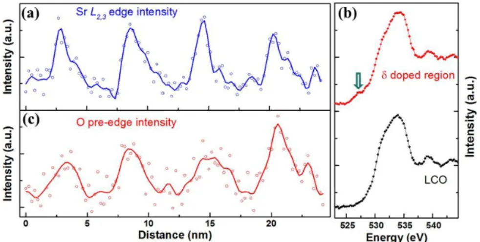
Atomic structure and local chemistry of Sr-δ-doped La
2CuO
4multilayers using aberration-corrected analytical STEM
Y. Wang1, W. Sigle1, D. Zhou1, F. Baiutti1, G. Logvenov1, G. Gregori1, G. Cristiani1, J. Maier1, P. A. van Aken1
1Max-Planck-Insititute for Solid State Research, Stuttgart, Germany
y.wang@fkf.mpg.de
Superconductivity in copper oxides arises when a parent insulator compound is doped beyond some critical concentration [1]. In the case of La2CuO4 (LCO), high-Tc superconductivity is obtained either by substituting La3+ with Sr2+ or by inserting interstitial O2- [2]. At internal interfaces, the enhancement of the superconducting critical temperature is influenced by the interfacial structure [3]. Recently, by using atomic layer-by-layer oxide molecular beam epitaxy (MBE), we have fabricated Sr-δ-doped LCO multilayered structures on LaSrAlO4 (LSAO) substrate, in which some atomic planes of LaO were intentionally substituted by SrO. By varying the spacing between the LCO and SrO layers high-Tc superconductivity (~ 40 K) was obtained [4]. In this study we focus on the detailed and quantitative scanning transmission electron microscopy (STEM) analysis in combination with energy-dispersive x-ray (EDX) analysis and electron energy-loss spectroscopy (EELS).
For the present contribution, we combine atomic-resolved quantitative STEM imaging with analytical STEM-EELS/EDX analysis to understand the occurrence of high-Tc superconductivity at Sr-δ-doped LCO interfaces with respect to the local lattice and oxygen octahedral distortion, as well as cation and electron hole redistribution. STEM investigations were performed using a JEOL JEM-ARM 200F scanning transmission electron microscope equipped with a cold field emission electron source, a DCOR probe corrector, a 100 mm2 JEOL Centurio EDX detector, and a Gatan GIF Quantum ERS electron energy-loss spectrometer.
Figure 1a shows a cross-sectional high-angle annular dark-field (HAADF) STEM image of Sr-δ-doped LCO multilayers, revealing that LCO and the LSAO substrate exhibit perfect epitaxy and show no local structural defects at the -δ-doped interfaces. From the HAADF image intensity, we can clearly see that the atomic column intensity in Sr-δ-doped region is lower than in pure LCO, due to the difference in the atomic number of La and Sr (ZSr=38, ZLa=57). The average image intensity profile in growth direction shows that at the Sr-δ-doped region the image intensity has a relatively sharp drop of intensity followed by a slowly increasing intensity pointing to an asymmetric Sr distribution. Atomic-resolved HAADF and ABF images, which were simultaneously acquired at the Sr-δ-doped region, are presented in Figs. 1b and 1c. In these images, all the atomic columns (La/Sr, Cu, O) have been resolved. The local lattice and copper-apical- oxygen distortions were quantitatively evaluated by image analysis and the association between these distortions and the superconductivity will be discussed.
A detailed study on the redistribution of Sr and of electron holes at the interface was performed by a combination of atomic-resolved STEM-EELS/EDX. The Sr-L EDX and Sr-L2,3 EELS (Fig.2 a) line-scan profiles show that Sr is redistributed over a few layers in LCO and has an asymmetric concentration profile.
The electron holes across the Sr-δ-doped interfaces were characterized by analysis of the O-K near-edge fine structure, as presented in Figs. 2b and 2c. A comparison of the Sr and electron holes profiles suggests a rather complex charge rearrangement mechanism which account for the occurrence of the high-Tc superconductivity. [5]
1. P.A.Lee et al., Rev.Mod.Phys. 78 (2006) 17 2. B.O.Wells et al., Science 277 (1997) 1067 3. A.Gozar et al., Nature 455 (2008) 782 4. F.Baiutti et al., submitted (2015)
5. The research leading to these results has received funding from the European Union Seventh Framework Program under Grant Agreement No.312483 (ESTEEM2). U. Salzberger is particularly acknowledged for TEM specimen preparation.
22
Figure 1. (a) HAADF image of Sr-δ-doped LCO multilayers epitaxially grown on a LSAO substrate. Simultaneously acquired (b) HAADF and (c) ABF images of one Sr-δ-doped region, on which the atomic columns have been marked for quantification of the lattice and copper-apical-oxygen distortions.
Figure 2. (a) Integrated Sr-L2,3 EELS line profiles across 4 Sr-δ-doped regions. (b) O-K edge from a Sr-δ-doped region and from LCO. (c) Integrated O-K pre-edge intensity profile across 4 Sr-δ-doped regions.
23
Functional Materials (magnetic, ferroelectric, ferroic, superconducting, electronics)
MS1.P006
Energy diffractive imaging and spectroscopy of ferromagnetic La
0.7Ba
0.3MnO
3thin films for resolving magnetic properties
X. Li1, I. Verjoiu1, P. A. van Aken1
1Max Planck Institute for Solid State Research, Stuttgart, Germany
xiaoyan.li@is.mpg.de
The development of quantitative magnetic characterization techniques down to the atomic scale promises a further progress in nanotechnology, such as for high density data storage. A reliable method to perform the magnetism measurement at such high spatial resolution is based on electron magnetic circular dichroism (EMCD) in a transmission electron microscope (TEM) - a novel method first developed by Schattschneider et al. in 2003 [1, 2]. Recently, an attractive technique of utilizing an astigmatic electron probe within a Cs- corrected scanning electron transmission microscope (STEM) was proposed by Rusz et al. [3], showing great potential for measuring EMCD with atomic resolution. Their calculation reveals that it is possible to obtain the EMCD signal in the transmitted beam directly without the necessity of producing electron vortex beams. The crucial feature is the relation between crystal structure, magnetic symmetry of the sample, and distribution of the phase in the electron beam. A certain amount of aberration should be introduced to obtain the required phase symmetry of the electron beam and to measure the non-zero EMCD signal in the transmitted beam. This magnetic signal reaches its maximum intensity (~1%) when the beam is passing directly through an atomic column, and drops dramatically when the beam is shifted away from the column (shift > ½ FWHM of the beam). Practically, by simply taking the difference of in-column and off-column spectra, or of different atomic columns with opposite magnetic moments (in anti-ferromagnetic materials), the EMCD signal can be extracted at the atomic scale.
In our work, we are aiming at obtaining the EMCD signal with atomic resolution experimentally. The work is firstly carried out on the La0.7Ba0.3MnO3 (LBMO) ferromagnetic thin films where the magnetism is provided by Mn. Since the properties of perovskite materials are closely related to their structures, the preliminary STEM study was carried out using a JEOL ARM200F under aberration-corrected conditions to gain insight into the structural and chemical nature of the thin film. The high-angle annular dark-field image in Fig. 1a shows a cross-sectional view of a perovskite SrRuO3 (SRO)/LBMO/SRO multilayer heterostructure on SrTiO3 substrate, where no structural defects are observed. Further atomically resolved EELS-based elemental mapping of Ti, La, Ba, Mn are acquired across the thin film, as shown in Fig. 1b, demonstrating a sharp non-diffusing interface between LBMO and its neighboring SRO layers. The electronic structure of Mn was probed across the LBMO layer by means of high-energy resolved ELNES at the Mn-L2,3 edges (Fig.
1c). The ELNES spectra extracted from the interfaces show the same features as the ones within the layer, indicating a well-defined homogeneous chemical structure of Mn. These low-defect microstructures can explain the good magnetic property of LBMO at such low thickness (2.5 μB/Mn). In future, EELS spectrum images with sub-Å pixel size will be recorded under aberrated probe conditions, together with accurate measurements of the aberrations, expecting for a possibly reliable EMCD signal [4].
1. C. Hebert, P. Schattschneider: Ultramicroscopy 96 (2003) 463 2. P. Schattschneider et al.: Nature 441 (2006) 486
3. J. Rusz, J.-C. Idrobo and S. Bhowmick, Phys. Rev. Lett. 113 (2014) 145501
4. The research leading to these results has received funding from the European Union Seventh Framework Programme [FP7/2007-2013] under grant agreement n°312483 (ESTEEM2). XL gratefully acknowledges Dr. Yi Wang for the introduction and support with the microscopic investigations
24
Figure 1. (a) STEM-HAADF image of the La0.7Ba0.3MnO3 ferromagnetic thin film. (b) STEM-HAADF image and corresponding STEM-EELS elemental maps of Ti, La, Ba, Mn for the heterostructure. (c) EELS spectra of Mn L2,3
extracted from every atomic layer of Mn.
25
Functional Materials (magnetic, ferroelectric, ferroic, superconducting, electronics)
MS1.P007
Magnetic structure of magnetite nanoparticles studied by electron holography
K. Vogel1, S. Sturm1, D. Wolf1, E. Rosseeva2, M. Helminger2, H. Cölfen2
1Technische Universität Dresden, Institut für Strukturphysik, Dresden, Germany
2University of Konstanz, Department of Chemistry, Konstanz, Germany
karin.vogel@triebenberg.de
Electron holography is a powerful tool for investigation of magnetic specimens because the phase of the electron wave is sensitive to magnetic fields within or around the sample. Here, we apply off-axis electron holography for characterizing the magnetic structure of magnetite nanoparticles. The particles had been synthesized to mimic the structure and properties of magnetite crystals in magnetotactic bacteria. These bacteria contain magnetite nanocrystals arranged along a chain within the bacteria. The magnetization of the nanocrystals is nearly parallel to the axis of the chain, as shown by electron holography [1]. The aim of our studies is to check whether the synthesised magnetite nanoparticles show similar properties like the “natural”
magnetite crystals within the bacteria.
The magnetite nanoparticles were synthesized using a precipitation method by slow addition of iron (II) sulfate solution to an aqueous solution containing the mixtures of potassium hydroxide and potassium nitrate (oxidizing agent). The synthesis was performed under nitrogen atmosphere. The resulting product was washed several times with degassed Milli-Q water and a drop of this suspension was placed on a TEM-grid.
For the holographic investigations we used a Philips CM200 TEM equipped with a Lorentz lens and an electrostatic biprism. The Lorentz lens allows investigating magnetic samples under virtually field-free conditions. The objective lens can be used to change the magnetization direction in the particles. After choosing a suitable chain of magnetite particles (Fig. 2a), the Fischione dual tilt tomography holder model 2050 was rotated to align the chain perpendicular to the tilt axis. Then, the specimen was tilted to +75 degree to achieve a large component of the magnetic field along the chain by switching on the objective lens. After a few seconds the objective lens was switched off, the holder was tilted back to zero, and the hologram was acquired under field-free conditions. To reverse the magnetization direction, the procedure was repeated with the specimen tilted to an angle of -75 degree.
From the holograms the complete electron wave in amplitude and phase was reconstructed. Figs. 1a and 1b show reconstructed phase images of the magnetite chain after exposition to external magnetic fields H in opposite direction. By comparing the phase profiles in Fig. 1c, it becomes evident that the magnetization direction in the chain has changed when the external magnetic field was reversed. Since the phase shift is not only influenced by the magnetic induction B, but also by the mean inner (electric) potential, we have to separate its magnetic and electric parts. This can be done by calculating half the difference and the sum of the two phase images shown in Figs. 1a and 1b. The separated magnetic phase contribution is shown in Fig.
2b. From the gradient of the magnetic phase, we obtained the induction map shown in Fig. 2c. The white lines in the map are lines of equal phase shift and correspond to the field lines of the projected B-field. The induction map reveals that the magnetization in the particles is aligned along the chain and the magnetic flux is closed by the stray field. The deviations in the lower part of the chain will be a subject of further investigation. Furthermore we will analyze the morphology of the magnetite particles using TEM tomography.
1. Dunin-Borkowski, R. E.; McCartney, M. R.; Frankel, R. B.; Bazylinski, D. A.; Posfai, M. & Buseck, P. R. Science, 1998, 282, 1868-1870.
2. We acknowledge the financial support from the European Union under the Seventh Framework Programme under a contract for an Integrated Infrastructure Initiative. Reference 312483 - ESTEEM2
26
Figure 1. a), b) Phase images of a chain of magnetite particles. The arrows indicate the direction of the external magnetic field H. c) Phase profiles across the chain and the polymer support.
Figure 2. a) TEM image of the magnetite chain. b) Magnetic phase contribution separated from the phase image shown in Fig. 1a. c) Color-coded magnetic induction map obtained from the gradient of the magnetic phase image. The color wheel indicates the direction of the magnetic induction.
27
Functional Materials (magnetic, ferroelectric, ferroic, superconducting, electronics)
MS1.P008
Cross-sectional TEM preparation of ZnO nanospikes for fundamental 3D defect analysis
N. Wolff1, V. Hrkac1, J. Ditto2, D. Smazna3, R. Adelung3, L. Kienle1
1Institute for Materials Science, Christian-Albrechts-Universität zu Kiel, Synthesis and Real Structure, Kiel, Germany
2University of Oregon, Department of Chemistry and Materials Science Institute, Oregon, United States
3Institute for Materials Science, Christian-Albrechts-Universität zu Kiel, Functional Nanomaterials, Kiel, Germany
niwo@tf.uni-kiel.de
A new concept for the realization of innovative magnetic field sensors with a limit of detection (LOD) smaller than 1 pT is based on the piezotronic read-out over a Schottky barrier of ZnO based magnetoelectric composites. Amongst morphology and doping concentration the ZnO crystal orientation and defects play a decisive role for the piezotronic properties, since they influence e.g. the conductivity and the height of the Schottky barrier. For monitoring such real-structure property relations, a three dimensional defect characterization is required. However, the strongly textured morphology inhibits wide-angle tilting experiments in TEM, and cross-sectional preparation of the one dimensional ZnO nanospikes is complicated by charging effects in FIB.
ZnO nanospikes prepared by the flame transport synthesis (FTS) method [1] have been subject of detailed plane-view investigations so far. Superposition twinning in nanospikes was investigated as an intrinsic real structural feature looking along [2-1-13] direction [2]. The observed twin boundary (TB) of a buried minority component is specified to be (2-1-11). Here, sophisticated cross-sectional preparation of ZnO nanospikes is achieved for the first time by selectively embedding them in amorphous carbon and subsequent cut and lift-out routine using the focused ion beam (FIB) technique. A novel shadowing technique was applied for careful thinning using the silicon substrate as a protective layer in order to minimize abrasion to the carbon film. Cross-sections of ZnO nanospikes are investigated using high resolution TEM. Closer inspection of the nanostructure (see Fig.1) reveals two common TB junctions. The TB junctions can be assigned to [2-1-10]/(01-13) and [2-1-10]/(01-11) having angles between the (0001) planes of 63.3° and 57°, respectively. Further, stacking mismatches and vacancies can be identified.
1. Mishra, Y. K., Kaps, S., Schuchardt, A., Paulowicz, I., Jin, X., Gedamu, D., Freitag, S., Claus, M., Wille, S., Kovalev, A., Gorb, S. N. and Adelung, R., Fabrication of Macroscopically Flexible and Highly Porous 3D Semiconductor Networks from Interpenetrating Nanostructures by a Simple Flame Transport Approach. Part. Part. Syst. Charact., 30, (2013), 775.
2. Hrkac, V.; Kienle, L.; Kaps, S.; Lotnyk, A.; Mishra, Y. K.; Schürmann, U.; Duppel, V.; Lotsch, B. V.; Adelung, R."Superposition twinning supported by texture in ZnO nanospikes," J. Appl. Cryst., 46, (2013), 396.
28
Figure 1. Exemplary cross-section of ZnO nanostructure in C matrix.
Figure 2. HRTEM micrograph of the cross-section presented in Fig.1. Stacking mismatches are indicated by arrows.
(orange) FFT of area containing a basal-plane stacking fault in [2-1-10] zone axis orientation. (green) [2-1-10]/(01-13) TB junction, FFT and kinematic simulation by superposition (rotation by 63.3°).