Resistivity Oscillations in GaAs Heterostructures
Dissertation
zur Erlangung des Doktorgrades der Naturwissenschaften (Dr. rer. nat.)
der Fakultät für Physik der Universität Regensburg
vorgelegt von Tobias Herrmann
aus Dresden
im Jahr 2019
Die Arbeit wurde angeleitet von: Prof. Dr. Sergey D. Ganichev
Prüfungsauschuss
Vorsitzender: Prof. Dr. Vladimir Braun
1. Gutachter: Prof. Dr. Sergey D. Ganichev
2. Gutachter: Prof. Dr. Christian Schüller
weiterer Prüfer: Prof. Dr. Josef Zweck
1 Introduction 3
2 Physical Background and Preliminary Works 6
2.1 Two-Dimensional Electron Gas . . . . 6
2.1.1 Band Structure of the Two-Dimensional Electron Gas . . 6
2.1.2 Electron Transport in Two Dimensions . . . 10
2.2 Radiation Induced Effects in Two Dimensional Electron Gases . . . 20
2.2.1 Cyclotron Resonance . . . 20
2.2.2 Electron Gas Heating . . . 23
2.2.3 Microwave Induced Resistivity Oscillations . . . 25
2.2.4 Displacement Mechanism and Inelastic Mechanism . . . 28
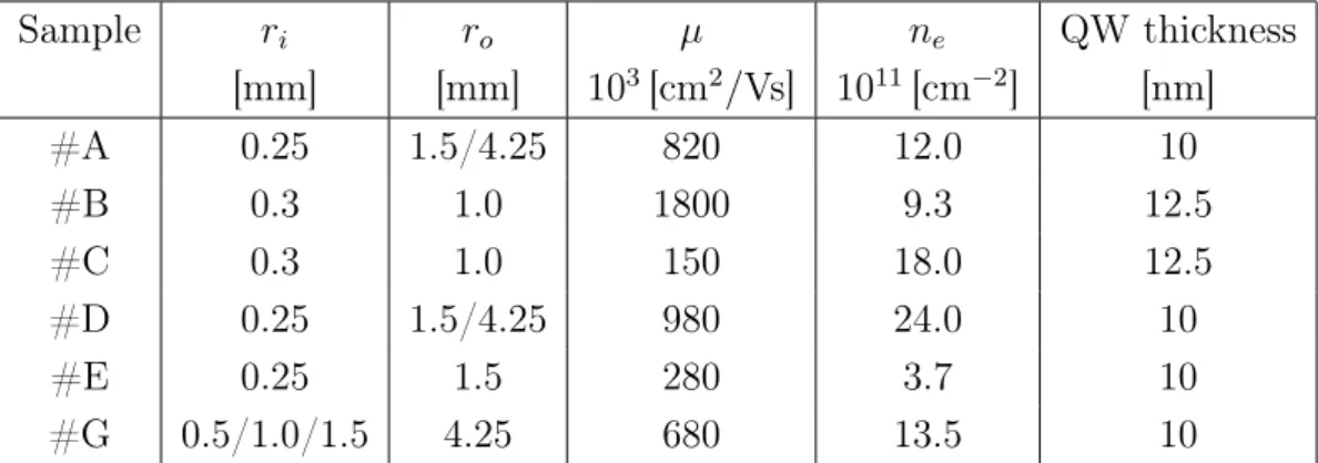
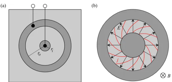
3 Methods 36 3.1 Investigated Samples . . . 36
3.1.1 Material Properties . . . 36
3.1.2 Corbino Geometry . . . 38
3.2 Experimental Technique . . . 39
4 Terahertz Radiation Induced Resistivity Oscillations 43 4.1 Terahertz Analogue of Microwave Induced Resistivity Oscillations . . . 43
4.1.1 Results . . . 43
4.1.2 Discussion . . . 47
4.2 Bulk or Boundary Origin of the Terahertz Radiation Induced Resistivity Oscillations . . . 52
4.2.1 Results . . . 52
4.3 Circularly Polarized Terahertz Radiation Induced
Resistivity Oscillations . . . 59 4.3.1 Results . . . 60 4.3.2 Discussion . . . . 61 4.4 High Intensity Terahertz Radiation Induced
Resistivity Oscillations . . . 63 4.4.1 Results . . . 63 4.4.2 Discussion . . . 68
5 Conclusion 77
References 79
Acknowledgements 86
The research on two dimensional electron gases (2DEG) has been playing a central role in solid state physics in the last fifty years, yielding major progress in semiconductor technology [1, 2] and fundamental research [3]. The Nobel Prize awarded integer [4] and fractional quantum Hall effect [5–7] are the most prominent examples of phenomena observed in such systems, both in a regime of strong magnetic fields, where a strong quantization has to be considered.
Not only in this regime fascinating effects occur. Also in the range of lower magnetic fields where classical or semi-classical approaches can be used. Two examples of such effects are the commensurability modifications of the resistance induced by periodic potentials, known as Weiss-oscillations [8, 9], and the magnetoresistance oscillations generated by external fields applied additionally to the magnetic field [10]. To the latter count, e.g. the Hall field induced resistance oscillations [11], the phonon induced resistance oscillations [12, 13], and the microwave induced resistivity oscillations (MIRO) [14]. Especially the observation of zero resistance states (ZRS) in the context of MIRO [15, 16]
has drawn a lot of attention. Many experimental works on MIRO have been reported over the last eighteen years [15–37]. Although several models have been developed [38–42], there is still no commonly accepted theoretical explanation of the phenomenon [43, 44]. In particular three open questions remain: Firstly, whether they are a phenomenon which occurs on the boundaries of a 2DEG and the respective contacts [45] or environment, which can be, e.g. air or vacuum [38], or whether it occurs in the whole 2DEG [42, 46]. Secondly, it has to be clarified how strongly the oscillations are influenced by the polarization of the applied radiation [23]. And as a third open question, the behavior of MIRO when illuminated with high intensity radiation was studied lately [29, 35] in the microwave range, but high intensity data induced by higher frequencies are yet to be obtained. Such data would demonstrate the robustness of the effect, even under extreme experimental conditions on the one hand and would help to understand the underlying mechanisms on the other.
This thesis is devoted to the study of radiation induced resistivity oscillations
in GaAs 2DEG, not induced by microwaves but by terahertz (THz) radiation.
Although most works on MIRO are performed in the microwave range, it was shown that MIRO-like oscillations can also be induced by high frequency radiation [32, 36, 37]. Here, the advantages of THz laser radiation, which are not present in the microwave range, are exploited to provide answers to the open questions in the field of MIRO. The study shows, that, indeed, the observed THz induced photoconductivity oscillations are MIRO. In this thesis also the question, whether the observed oscillations originate from the sample boundaries, or whether the effect stems from the whole 2DEG, is answered.
This allows to determine which of the theories addressed above can be employed on the observed oscillations. In the following the results are analyzed in the framework of those theories. Furthermore, the helicity dependence of MIRO is intensely studied. The analysis shows that the influence of the radiations helicity is weaker than theoretically expected. Consequently, possible reasons for this discrepancy are discussed. Furthermore the study reports on the irradiation of GaAs 2DEG with high power radiation. There, MIRO are observed for several frequencies and in a intensity range of five orders of magnitude. Based on these observations the corresponding saturation mechanisms are discussed.
In detail, this thesis is structured as follows: Chapter 2 is devoted to the physical background of MIRO and an overview over preliminary works on the topic. It starts with a general description of a 2DEG in Sec. 2.1.1 and with the mechanisms describing magnetotransport in such a system in Sec. 2.1.2.
Afterwards radiation related phenomena in a 2DEG are discussed, including cyclotron resonance (CR) in Sec. 2.2.1 and electron gas heating in Sec. 2.2.2.
Finally, in Sec. 2.2.3, MIRO are discussed on the basis of preliminary works on this effect and the displacement and the inelastic mechanism are introduced in Sec. 2.2.4. The second chapter gives an overview over the applied methods.
It starts with the description of the probed samples in therms of material properties and the used contact geometries in Secs. 3.1.1 and 3.1.2, respectively.
Afterwards the radiation sources and the different experimental setups used
in this work are described in Sec. 3.2. In chapter 4 the experimental results
are presented and discussed. The first part, Sec. 4.1.1 is devoted to the
presentation of the photoconductivity data featuring THz induced magneto-
oscillations Then, it is demonstrated that the observed oscillations feature
exactly the same properties as MIRO in Sec. 4.1.2, which in turn allows to treat
them as the same effect. In the following section, 4.2.1, the oscillations are
studied by selective illumination of either only the bulk or the boundaries. The
results show, that MIRO is a bulk effect, which in turn allows on to conclude
which theory describes the observed oscillations best. Consequently the data
is analyzed in therms of the respective mechanisms in Sec. 4.2.2. Afterwards
the helicity dependence of MIRO is studied in Sec. 4.3.1 and the results for
different polarizations are discussed in Sec. 4.3.2. In Sec. 4.4 photoconductivity
oscillations induced by high intensity THz radiation are presented. They show
a strong saturation for high intensities. The underlying saturation mechanisms
are discussed in Sec. 4.4.2. Finally, chapter 5 summarizes the work and gives
an outlook to further research on MIRO.
This chapter’s purpose is to introduce the fundamental principles necessary to get an understanding of this work. Therefore a short introduction to the dimensional electron gases (2DEG), the systems in which MIRO are observed is given. Afterwards the carrier transport and radiation absorption in a 2DEG will be discussed. The last part of this chapter is devoted to give an overview of both experimental and theoretical preliminary work on MIRO.
2.1 Two-Dimensional Electron Gas
Two dimensional electron gases play a crucial role when it comes to designing high mobility semiconductor structures, which are of tremendous importance in modern electronic technology [1, 2]. Their role in solid state physics, however, is not less important. The quantum Hall effect [4] is, for instance, a fundamental effect discovered in a 2DEG. The following example for the band engineering of a 2DEG is adapted from Ref. [47].
2.1.1 Band Structure of the Two-Dimensional Electron Gas
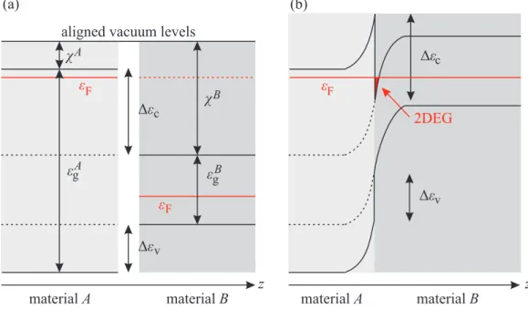
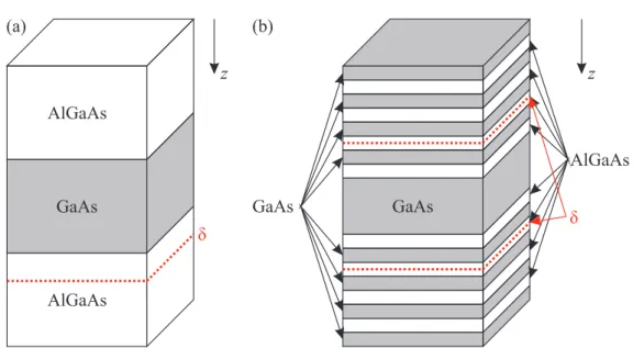
A 2DEG can be realized when two semiconductor materials with different band gaps but similar lattice constants are stacked on top of each other. Figure 1 (a) shows the band structures of two such semiconductors, A and B, before assembly.
Following Anderson’s rule the vacuum levels of the two materials line up [47].
The vacuum level alignment leads to potential differences ∆ε
cand ∆ε
vfor both,
the conduction and the valence band. When the two materials are assembled
and if they are doped, for example one p- and one n-typed, a charge transfer
takes place. This leads to the formation of a dipole layer and, correspondingly,
to that to a band bending at the heterojunction. Figure 1 (b) shows this for
the two exemplary materials. Here, the one with the large band gap ε
Agis
n-doped, whereas the one with the smaller gap E
gBis slightly p-doped. When
thermal equilibrium is achieved the Fermi levels are matched up in the region
of the junction. If the new Fermi level is now higher than the minimum of
the bended conduction band, electrons are trapped in a potential well being
roughly triangular. ∆ε
cprevents electrons and holes from recombining and the electrostatic potential in between squeezes the electrons towards the interface.
The potential well is usually about 10 nm thick, and the electron movement is restricted in growth direction of the semiconductor structure. The growth direction is defined as z in this work. In the orthogonal directions x and y, however, the electrons can move freely. This is the two-dimensional electron gas. This method of growth with the donors lying at a distance from the 2DEG is referred to as modulation doping and yields two main benefits: besides the confinement of electrons to two directions addressed above, the donors and electrons are separated, and therefore scattering by ionized impurities is reduced and high mobilities can be achieved.
Δε
vΔε
cε
g Aε
g BΔε
cΔε
v2DEG
(a) (b)
aligned vacuum levels χ
Aχ
Bz z
material A material B material A material B
ε
Fε
Fε
FFigure 1: Conduction and valence bands of two semiconductors, A and B, before (a) and after (b) thermal equilibration. The material growth direction is represented by z. Vacuum levels are aligned, shown in panel (a) following Anderson’s rule. (b) Fermi levels are aligned yielding a band bending, leading to a roughly triangular potential well. Adapted from [47].
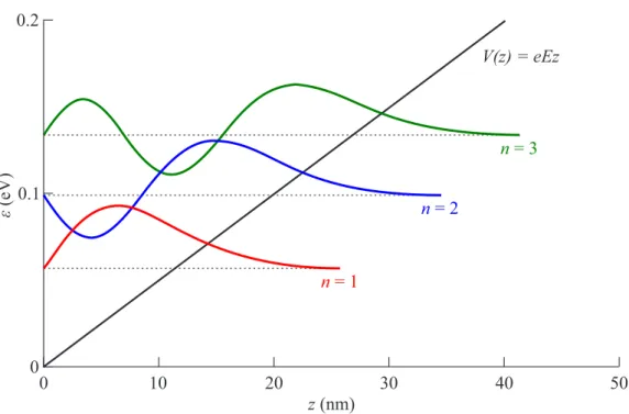
The restriction in z yields an energy quantization of the electrons in the 2DEG
which is discussed in the following. To calculate the electron wave functions and
their energy eigenvalues the 2DEG potential will be approximated as a perfect
triangular potential well. For simplification the potential barrier at z < 0 is defined as finitely high. For z > 0 a linear potential V (z) = eEz is assumed.
It describes an electron of the charge e in an electric field E. The free carrier motion in the 2DEG plane is not related to the confinement in z-direction.
Hence a product approach to the wave function can be taken, which reads as
ψ(rrr) = e
ikxxe
ikyyφ(z). (1)
With φ(z) being the z-dependent part of the wave equation, one can write the one dimensional Schrödinger’s equation [47]
− ~
22m
∗zd
2dz
2+ eEz
φ(z) = εφ(z). (2)
In order to solve it the dimensionless quantities z ¯ = z/z
0and ε ¯ = ε/ε
0are defined, where
z
0= ~
22meE
1/3, ε
0=
(eE ~ )
22m
1/3= eEz
0. (3)
Schrödinger’s equation reduces now to the Airy equation [47]
d
2φ
ds
2= sφ, (4)
with the new independent variable s = ¯ z − ε. The Airy equation has two ¯
independent solutions Ai(s) and Bi(s) [47]. Two requirements have to be
fulfilled in order to obtain an applicable solution: The boundary condition at
z = 0 requires φ(z = 0) = φ(s = −ε
0) = 0. Both Airy functions oscillate for
negative (s), and consequently the energies of the bound states of the triangular
well are found for the functions being zero. Moreover the wave function should
be well defined for z → +∞. Therefore, the solution Bi(s) can be neglected,
since it diverges for s → +∞ [48]. For Ai(s) however there is an infinite number
n of negative s-values where it equals zero, which are called −c
nhere. To make sure that φ(z = 0) = 0 is fulfilled, ε ¯ = c
nis necessary and the allowed energies are given by
ε
n,z= c
n(eE ~ )
22m
∗z 1/3, with n = 1, 2, 3, ... , (5) and m
∗zbeing the effective electron mass in z-direction.
0.2
0.1
0
ε (eV)
0 10 20 30 40 50
z (nm)
V(z) = eEz
n = 1
n = 2
n = 3
Figure 2: Energy levels (dashed lines) and corresponding wave functions (colored solid lines) of a triangular potential well with potential energy V (z). The scales are for electrons in GaAs and an electric field E = 5 MV m
−1. Adapted from [47].
The respective unnormalized one dimensional wave functions are
φ
n(z) = Ai(s) = Ai
eEz − ε ε
0. (6)
Following the product approach in Eq. (1), the three dimensional energy eigen-
values are given by
ε
i(k
x, k
y) = ε
n,z+ ~
2k
x22m
∗x+ ~
2k
y22m
∗y, (7)
containing the effective electron masses m
∗x, m
∗y, and the electron wave vectors k
xand k
y[47].
2.1.2 Electron Transport in Two Dimensions
This work is devoted to study the influence of external experimental parameters like magnetic fields and terahertz radiation on the electron motion in a 2DEG.
The microscopic description in this section will mainly follow the logic of Ref.
[49]. When it comes to electron motion Ohm’s law
jjj(rrr) = σE E E(rrr) (8)
is best to start with. It states that the electric current density jjj(rrr) and the electric field E E E(rrr) driving the electrons, are proportional to each other.
The constant linking them together is the electrical conductivity σ, which is independent on the direction rrr in a homogeneous conductor.
Though, the electrical conductivity depends on the conducting material, the material shape determines whether the electrons can move in three or just two dimensions. From a microscopic perspective, the material dependence of the conductivity is described by the Drude model and based on the scattering probability of an electron in the respective material. Scattering is possible, i. a.
with crystal defects, or phonons.
In this work two fields are applied: An electric field in the 2DEG plane, for instance E E E = (E, 0, 0), and a magnetic field B B B = (0, 0, B) perpendicular to it.
The electrons are then accelerated by the Lorentz force F F F = −eE E E − ev v v × B B B and the motion between two scattering events can be described by Newton’s equations
dv
xdt = − |e|
m
∗(E + v
yB),
dv
ydt = + |e|
m
∗v
xB. (9)
These equations can be rewritten as
dv
xdt = −ω
c(v
D+ v
y),
dv
ydt = +ω
cv
x. (10)
introducing the cyclotron frequency ω
c= |e|B
z/m
∗and the drift velocity v
D= E/B. The solution of Eq. (10) is
v(t) = 0
−v
D!
+ v
y(0) + v
D−v
x(0)
!
sin(ω
ct) + v
x(0) v
y(0) + v
D!
cos(ω
ct). (11) Here t = 0 represents the time when the last scattering event took place leaving the electron with the velocity (v
x(0), v
y(0). The first term on the right hand side describes the drift motion, which is normal to the magnetic and the electric field direction. The second and third term represent a circular motion with the frequency ω
c, called cyclotron motion. The electron transport is strongly influenced by the cyclotron motion, being controlled by the product of cyclotron frequency and the average scattering time τ
q. In the case of small magnetic fields, i.e. ω
cτ
q1, the electrons can not complete a full cyclotron orbit without being scattered. The case ω
cτ
q1, in which one or even multiple cyclotron orbits are completed yields some drastic differences compared to the first case, as will be discussed later in this section.
On large time scales t τ
qthe electron will perform a drift motion. Under the
assumption that an electron has as drift velocity v
0in a random direction after
a collision which is independent of the direction before the scattering the drift
velocity can be calculated. Following this assumption the probability P (ϕ)dϕ
that the electron moves into direction ϕ after the collision is expressed by
P (ϕ)dϕ = dϕ/2π. (12) Additionally to the direction the time until the next scattering event has to be considered. The rate equation dP (t)/dt = −wP (t), which correlates the probability P (t) that an electron has not been scattered until the time t and the probability wdt that an electron is scattered within an infinitesimal time interval dt, has the solution P (t) = Ce
−wt. Here C = 1 can be derived from the initial condition P (0) = 1. The probability that the electron scatters within the time interval [t, t + dt] is given by the product p(t) = P (t)w(t). The mean scattering time is now
τ
q= Z
∞0
dtwe
−wtt = 1 w , and
p(t)dt = e
−t/τqdt
τ
q. (13)
From Eq. 10 one obtains the drift velocity by multiplying v with the probabilities P(ϕ)dϕ and p(t)dt and integrating over t and ϕ, which reads as
¯ v =
Z
2π0
dϕP(ϕ) Z
∞0
dtp(t)v(t). (14)
Consequently, the components of the drift velocity are given by
¯
v
x= −v
Dω
cτ
q1 + ω
2cτ
q2= −E
x|e|τ
q/m
∗1 + ω
c2τ
q2,
¯
v
y= −v
Dω
c2τ
q21 + ω
c2τ
q2= −v
D1 − 1 1 + ω
c2τ
q2. (15)
Note that for zero magnetic field strength B the mean drift velocity vanishes in y-direction, and reduces to a zero magnetic field value induced by the applied electric field in direction of x. The proportionality constant connecting the electric field and the drift velocity ¯ v
xat B = 0 is the mobility, given by
µ = |e|τ
pm
∗, (16)
with the transport lifetime, given by
τ
p−1= Z
2π0
dϕ(1 − cos(ϕ))P (ϕ). (17)
From equation (15) one immediately sees the properties of the Hall effect:
Under orthogonal application of an electric field and a magnetic field, the direction of the average electron drift deviates from the electric field direction by the Hall angle θ, obeying
tan θ = v ¯
y¯
v
x= ω
cτ
p= µB. (18)
The current density is given by
j
x= −n
s|e|¯ v
x= n
se
2τ
pm
∗1
1 + ω
c2τ
p2E
x,
j
y= −n
s|e|¯ v
y= n
se
2τ
pm
∗ω
cτ
p1 + ω
2cτ
p2E
x. (19)
Applying this result to Ohm’s law, see Eq. (8), one asserts that at finite
magnetic field normal to the 2DEG plane, the conductivity is a second rank
tensor with the components
σ
xx= n
se
2τ
pm
∗1 1 + ω
c2τ
p2σ
xy= n
se
2τ
pm
∗ω
cτ
p1 + ω
2cτ
p2. (20)
The missing tensor components can be taken from the same calculation as above but for an electric field in y-direction. This gives σ
yy= σ
xxand σ
yx= −σ
xy. Ohm’s law can now be written as
j
xj
y!
= σ
xxσ
xy−σ
xyσ
xx! E
xE
y!
. (21)
Note that Ohm’s law can also be written in terms of resistivity
E
xE
y!
= ρ
xxρ
xy−ρ
xyρ
xx! j
xj
y!
. (22)
with the resistivity tensor ρ being the inverted conductivity tensor
ρ
xxρ
xy−ρ
xyρ
xx!
= σ
xxσ
xy−σ
xyσ
xx!
−1= 1
σ
xx2+ σ
xy2σ
xx−σ
xyσ
xyσ
xx!
. (23)
With rising magnetic fields additionally quantization effects have to be taken into account and µB = ω
cτ
p1. This means that electrons complete multiple cyclotron orbits. Since the electron has also a wave character, it can interfere with itself. This interference is constructive for a certain phase and, therefore, it splits the former constant density of states n
DOSof the 2DEG into discrete energy levels ε
l, called Landau levels.
In order to get the values of the Landau levels, Schrödinger’s equation for the
potential V (z) under influence of an external magnetic field
1
2m
∗(p p p + eA A A)
2+ V (z)
ψ = εψ (24)
has to be solved. For a magnetic field B B B = (0, 0, B ) normal to the 2DEG plane one obtains the vector potential A A A = (A
x, A
y, 0). Similar to the procedure in Sec. 2.1, a product approach
ψ(x, y, z) = θ(x, y)φ(z) (25)
is chosen where the in- and out-of-plane Hamiltonians get separated, yielding the equations
1 2m
∗(p
x+ eA
x)
2+ (p
y+ eA
y)
2θ(x, y) = ε
xyθ(x, y) (26) and
1
2m
∗p
2z+ V (z)
φ(z) = ε
zφ(z) (27)
with ε = ε
xy+ ε
z.
Equation (27) is identical to Eq. (2), the one dimensional Schrödinger’s equation from Sec. (2.1), with the subband energies ε
ifrom Eq. (5) representing the eigenvalues ε
z. For simplicity the vector potential A = (−yB, 0, 0), known as the Landau gauge, is chosen and inserted to Eq. (26). This gives
1 2m
∗p
2y+ (p
x− eBy)
2θ(x, y) = ε
xyθ(x, y). (28) To solve this equation, again a separation approach
θ(x, y) = e
ikxxη(y) (29)
is used. Together with ω
c= |e|B/m
∗and p
x= −i ~ (∂/∂x)e
ikxx= ~ k
x, Schrö- dinger’s equation now reads
"
p
2y2m
∗+ m
∗2 ω
c2~ k
xeB − y
2#
η
kx(y) = εη
kx(y), (30) which is the equation for a one-dimensional harmonic oscillator with the potential minimum shifted by the value y
0=
~eBkx. For this equation the eigenstates are
ε
l= ~ ω
c(l + 1/2), l = 0, 1, 2, .. . (31) The quantized energy is independent of k
x, hence all states with different k
xbut the same l are degenerate. These degenerate states together form a Landau level. The density of states n
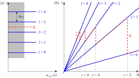
DOS(ε), which is continuous for free electrons and represented by the gray box in Fig. 3 (a), is replaced by a sequence of δ-functions at the Landau levels, represented by the blue lines. The total energy of the system consists of the three different contributions
ε
i,l,s= ε
z,n+ ε
xy,l+ sg
∗µ
BB. (32)
In this equation ε
z,idescribes the energy subbands due to the confinement in z-direction and ε
xy,lthe Landau levels. The additional term describes the energy difference due to spin splitting with s = ±1/2 being the spin quantum number, g
∗being the effective Landé-factor, and µ
Bbeing Bohr’s magneton.
Since spin does not play a role in this work, the last term will be neglected in the following considerations.
Since the cyclotron frequency ω
cdepends linearly on B, so does the Landau level separation, see Fig. 3 (b). They are highly degenerate and carry the number
n
l= n
DOS(E) ~ ω
c= g
seB
h (33)
ν = 2 l = 0
l = 4 l = 3 l = 2
l = 1
ν = 6 ν = 4 B
ε ε
n
DOS(ε)
E
FE
Fl = 0 l = 4 l = 3 l = 2 l = 1 ħω
c(a) (b)
Figure 3: Energy of the first Landau levels for the lowest subband (n = 1) as a function of (a) the density of states n
DOSand (b) the magnetic field B. Panel (a) shows that the energy levels, represented by the blue lines, are equidistant, separated by the factor ~ω
c. The electron distribution for free electrons is sketched by the gray box. In panel (b) the Fermi energy oscillates as function of the filling factor ν for fixed carrier density n
e. Adapted from refs. [47, 49].
of states per unit area and per spin orientation. If the s pin degeneracy is not lifted the Landé factor g
sequals two. The filling factor
ν = 2n
e/n
l= hn
e/eB (34)
compares the number of total electrons n
ein the system to the number of states per Landau level n
l. In experiment, with increasing magnetic field, ~ ω
cand consequently n
lalso increase. Since n
eis constant, the number of occupied Landau levels decreases for rising magnetic fields and the Fermi energy drops to deeper Landau levels at even filling factors ν, if the spin degeneracy is not lifted.
In the beginning of this section the classical description of the E E E × B B B drift has
been presented. This drift has to be considered also in the quantum mechanical
picture presented above. The applied electric field E E E = (0, E, 0) appears in Schrödinger’s equation as an electrostatic potential V (y) = eEy. The problem can, again be solved in analogy to the harmonic oscillator. However, the center coordinate is now modified to y ˜
0= ( ~ k
x+ m
∗v
D)/eB, with v
Dbeing the classical drift velocity. The Landau levels are then described by
ε
l(k
x) = ~ ω
c(l + 1/2) + eE
yy ˜
0+ m
∗v
D2/2, (35) containing the additional potential term eE
yy ˜
0and the kinetic energy m
∗v
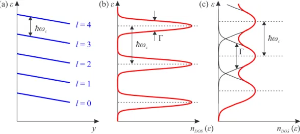
D2/2 from the drift motion. In real space, the additional terms result in a tilt of the Landau levels, as depicted in Fig. 4 (a).
ε (b) ε
y (a)
l = 0 l = 4 l = 3 l = 2 l = 1 ħω
cε (c)
ħω
cΓ ħω
cΓ
n
DOS(ε) n
DOS(ε)
Figure 4: Landau levels in real space representation under application of an electric field E in y-direction are presented in panel (a) and adapted from Ref. [49]. The density of states n
DOSin a magnetic field is presented in panels (b) and (c), showing Landau level broadening due to scattering. Distinct Landau levels for ~ ω
c> Γ in (b) and overlapping Landau levels for ~ ω
c< Γ in (c). Adapted from Ref. [47].
Generally, the description of the Landau levels as δ-functions is only valid for
ideal systems, where scattering, i.e. on other electrons, impurities, or phonons
is not present. In real systems at finite temperatures T 6= 0, however scattering
has to be taken into account. The finite lifetime τ
qdefines how long an electron
remains unscattered in a system. Note that it differs from the transport lifetime
τ
p= µm/e. While all collisions contribute equally to τ
q, the change of direction of the electrons influences the contribution to τ
pstrongly.
The finite lifetime τ
qresults in an energy uncertainty Γ = ~ /τ
qfor the Landau levels. The precise shape of the real system Landau levels is assumed to be of either elliptic or Lorentzian shape or a combination of both [49]. For all cases, it is important how Γ relates to the Landau level separation ~ ω
c. For strong magnetic fields ~ ω
c> Γ, the Landau levels are separated and quantum mechanical effects have to be taken into account, see Fig. 4 (b). For low fields the Landau levels overlap and the density of states can be attributed as constant with a periodic modulation, see fig 4 (c). Experimentally this periodic oscillation can, for instance, be observed as 1/B periodic oscillations of the longitudinal magnetoresistivity ρ
xx, called Shubnikov-de Haas (SdH) oscillations.
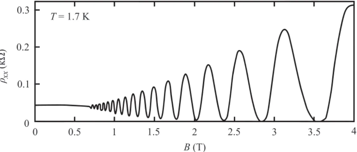
ρ (k Ω )
xx0 0
2 3 4
1 0.3
0.2
0.1
B (T) T = 1.7 K
3.5 2.5
1.5 0.5
Figure 5: Shubnikov-de Haas oscillations in the longitudinal resistivity ρ
xxof a 2DEG in a 10 nm GaAs quantum well. The measurement was performed at the temperature T = 1.7 K. Adapted from [49].
The longitudinal resistivity in the low-magnetic-field SdH-regime is given by [49]
ρ
xx(B, T ) = m
∗n
ee
2τ
p1 − 2e
−π/ωcτq2π
2k
BT / ~ ω
csinh(2π
2k
BT / ~ ω
c) cos
2π hn
e2eB
. (36)
This equation can be interpreted by looking separately at its components.
The magnetoresistance oscillates 1/B -periodically around the B-independent classical Drude resistivity, which is given by the prefactor. The term in the brackets represents the low-magnetic-field thermodynamic density of states for the broadened LL. It is assumed that the broadening is of Lorentzian shape.
Consequently, the oscillatory behavior of the longitudinal resistivity reflects at low magnetic fields the density of states at the Fermi energy. The exponential Dingle factor takes into account the finite lifetime broadening of the LL. For low magnetic fields the separation of the LL ~ ω
cis much smaller than the broadening Γ and the modulation amplitude gets strongly reduced. The energy averaging over k
BT around the Fermi level leads to a reduction of the SdH oscillations’ amplitude by temperature. The Fermi energy is assumed to be constant here. For higher magnetic fields this approximation is not valid, since the Fermi energy jumps when the modulation of the density of states is strong or a regime of separated LL is reached [49]. As Eq. 36 shows, the electron density n
e, as well as the quantum lifetime τ
qcan be determined from SdH oscillations observed in transport experiments.
2.2 Radiation Induced Effects in Two Dimensional Electron Gases
In the previous section the band structure of a 2DEG and the transport phenomena in crossed electric and magnetic fields are discussed. The physics of such a system exposed to electromagnetic waves are in the focus of the following section. Cyclotron resonance (CR) and electron gas heating are discussed in the first two subsections followed by the core topic of this thesis, microwave induced resistivity oscillations in the third subsection.
2.2.1 Cyclotron Resonance
The effect of cyclotron resonance describes the resonant absorption of radiation
with an angular frequency ω = ω
cby carriers moving on a cyclotron orbit
in a magnetic field B . The x-y-plane is defined as the plane of movement
in this section. The phenomenon of CR can be approached either quantum
mechanically as resonant absorption between the Landau levels [50] or classically [51, 52]. Here the classical approach is used. As described in Sec. 2.1.2 electrons are driven on cyclotron orbits by the Lorentz force due to a perpendicular magnetic field. When radiation with an electric field, lying in the cyclotron orbit plane and an angular frequency ω = ω
cis incident on the material, it is resonantly absorbed by the moving electrons. The equation of motion of the electrons is
m
∗dv v v
dt = e(E E E + v v v × B B B) − m
∗v v v
τ
p, (37)
with the effective mass m
∗of the electron in the semiconductor, the carrier drift velocity v v v, the electron charge e, the electric field E E E, the magnetic field strength B B B, and the momentum lifetime τ
p[52]. The current density components can be expressed as j
i= nev
iusing the carrier density n
eand i = x, y. The absorbed energy density per unit time P is obtained from the Joule losses formula
P = Re(J J J ) · Re(E E E) = 1
2 Re(J J J · E E E
∗), (38) with Re denoting the part of a complex number. Equation (38) shows that the orientation of the electric field of the incident electromagnetic wave is of special importance for the energy transfer. In this thesis the focus lies on circularly right- and left-handed polarized radiation, which will be elaborated on in the following. The radiation is assumed to be propagating along z-direction with an angular frequency ω. For right-handed circular polarization the electric field vector acts as
E
xE
y!
= E
0e
iωt−iE
0e
iωt!
= E
x1
−i
!
. (39)
The absorbed power density per unit time for this polarization then reads as
P = σ
0E
02(ω + ω
c)
2τ
p2+ 1 . (40)
For left-handed circular polarization the electric field vector is given by
E
xE
y!
= E
0e
iωtiE
0e
iωt!
= E
x1 i
!
(41) and consequently, the power density is
P = σ
0E
02(ω − ω
c)
2τ
q2+ 1 (42)
which only defers from Eq. 40 by the sign in the bracket. Remember, that the cyclotron frequency is defined as ω
c= eB
z/m
∗, which means that cyclotron resonance for right-handed helicity only occurs if the incident electromagnetic wave moves parallel to the magnetic field vector and for left-handed helicity only when the magnetic field is turned into the opposite direction of the incoming electromagnetic wave. This is a specific characteristic for the case of circularly polarized light. The helicity at which cyclotron resonance absorption occurs for a given magnetic field direction is addressed as CR active (CRA) polarization, whereas the one with no absorption is addressed as CR inactive (CRI). For linearly polarized radiation CR occurs in both magnetic field directions [52].
CR studies are usually carried out in absorption experiments. Under ideal conditions the transmission signal drops to zero for circularly polarized radiation and to ≈ 50 % for linear polarization at the CR magnetic field position B
CR. By fitting the slope of the CR-absorption signal with a Lorentzian the momentum relaxation time τ
pcan be extracted as the full width at half minimum. However, CR can also be observed in conductivity measurements. In order to evaluate how the absorbed power impacts the conductivity, the conductivity tensor elements from Eq. (20) have to be changed to [53]
σ
xx= σ
yy= e
2n
eτ
pm
∗τ
q−1+ iω (τ
p−1+ iω)
2+ ω
c2σ
xy= −σ
yx= e
2n
eτ
pm
∗ω
c(τ
p−1+ iω)
2+ ω
c2. (43)
Note, that for simplicity an energy distribution of the electrons is not taken into account here and that for ω = 0 the above equations equal the original tensor elements, see Eq. (20). For right-handed circular polarization the conductivity is given by [53]
σ
+= σ
0τ
p−1τ
p−1+ i(ω + ω
c) , (44)
and for left-handed circularly polarized radiation as [53]
σ
−= σ
0τ
p−1τ
p−1+ i(ω − ω
c) . (45)
2.2.2 Electron Gas Heating
The previous section is devoted to the CR and it is shown that it also influences the conductivity σ. In the following the effect of electron gas heating is discussed, which can affect the conductivity strongly, especially if the incident radiation has a high intensity I.
The carriers in an electron gas permanently exchange energy with the lattice.
If additional energy is delivered to the electrons it is transfered to the crystal by exchange mechanisms such as electron-phonon scattering. For high tem- peratures these transfer mechanisms are so effective, that the electrons are considered to be in thermal equilibrium with the lattice. At low temperatures, however, the coupling between charge carriers and the crystal can be much weaker. When the electrons exchange energy very effectively among each other, i.e. that the electron-electron interaction time τ
eeis much shorter than the energy relaxation time, their distribution can be described by an effective temperature T
ewhich is higher than the lattice temperature T
l[54]. This is particularly the case at high carrier densities n
e[55].
The change of carrier energy distribution by incident radiation results in a
change of mobility and accordingly a variation of the sample conductivity. The
balance equation
K(ω)Iε
ef f~ ω = hQ(T
e)i
n(46)
determines the electron temperature T
ebased on the relation between absorbed energy and the energy loss rate hQi = hdε/dti. The absorbed energy depends on the absorption coefficient K(ω), the intensity I and ε
ef f, which is the effective energy that one photo-excited electron contributes to the system [55].
As mentioned above the increase in T
eleads to a change in mobility µ. The associated conductivity modification is referred to as µ-photoconductivity and described by the equation [55]
∆σ σ = 1
µ
∂µ
∂T
eTe=Tl
∆T
e. (47)
In GaAs quantum wells high intensity THz excitation can lead to strong saturation effects [56, 57] of the photoconductivity due to scattering with longitudinal optical (LO) phonons. The energy transfer rate hQi in this case is exponentially dependent on T
e[55], given by
hQi = ~ ω
LOτ
ε,LOexp
− ~ ω
LOk
BT
e. (48)
Here the growing number of electrons, which are energetic enough to emit LO- phonons of the energy ~ ω
LOlifts the electron-gas temperature and consequently hQi. The emission rate is denoted as τ
ε,LO−1. In comparison to the LO-phonon emission rate of the electrons, the anharmonic decay rate for LO phonons is slow. Hence the energy transfer from electrons to phonons can produce a number of non-equilibrium phonons which results in a saturation of ∆σ/σ at high I.
Not only the mobility µ is affected by the electron gas temperature. It was
shown in Sec. 2.1.2, that the quantum lifetime τ
qis significantly changed
when the lattice temperature T
lis increases, resulting in a decline in SdH
oscillation amplitude. The same effect can also be observed, when due to
high intensity illumination the electron gas is heated, which is reasonable considering that the main mechanism limiting τ
qin high mobility 2DEGs is electron-electron scattering [58]. However, it has to be addressed that the effect is weaker for rising T
eas for T
l, since less phonons are involved in the first case. The reduction of the SdH oscillation amplitude is also measured as photoconductivity oscillations under illumination with high intensity radiation.
The oscillations occur at the same magnetic field values as the SdH oscillations obtained in magnetotransport experiments.
2.2.3 Microwave Induced Resistivity Oscillations
In the previous sections two photoconductivity effects based on different mi- croscopic mechanisms are discussed. Zudov et. al reported on a completely new photoconductivity phenomenon in 2001 [14]. By applying microwave radiation to high mobility (µ ≥ 3.0 × 10
6cm
2/Vs) GaAs 2DEGs, oscillations of the longitudinal conductivity are observed at low magnetic field values, where contributions of CR and SdH oscillations are not expected. By using ultra high (µ ≈ 1.5 × 10
7cm
2/Vs) mobility 2DEGs in 2002 Mani et al. where able to increase the oscillation amplitude such strongly that they where able to observe zero resistivity states [15]. Both publications attracted a lot of interest and stimulated a high number of works on the topic of MIRO in the following decade.
The original results of Zudov et al. are presented in Fig. 6, showing oscillations that are, just like the SdH oscillations, 1/B periodic and hence where called
"SdH-like"[14]. However, they occur at much weaker magnetic fields, where the Landau levels are not yet strictly separated. Their period is governed by the ratio of = ω/ω
c∝ 1/B, with ω being the microwave frequency and ω
cbeing the cyclotron frequency. Figure 7 (b) shows MIRO as a function of . The maxima
+and minima
−are roughly symmetrically offset from the harmonics of the cyclotron resonance at integer and occur at
±= ∓ ϕ. (49)
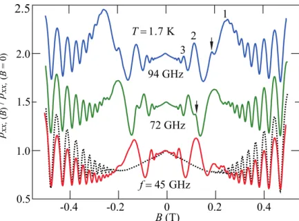
GHz f ����
72 GHz 94 GHz
�
�
� T ����� K 2.0
1.0 1.5
0.5 2.5
B (T) ρ
xx, (B)/ ρ
xx,(B = 0)-0.4 -0.2 0 0.2 0.4
Figure 6: Magnetoresistivity ρ
xx,Bwith (solid lines) and without (dashed lines) microwave illumination for different frequencies f = 45, 72, and 94 GHz normalized to its zero magnetic field strength value ρ
xx,B=0. Data for different frequencies are vertically offset for better visibility. Integer numbers denote maxima corresponding to the order of MIRO
+. The data is obtained at T = 1.7 K in a Hall bar sample.
Adapted from [14].
The value of the phase is reported as ϕ = 1/4 in many experiments [17–19].
For low harmonics, measurements show that the extrema move towards integer yielding a phase smaller than 1/4 [21, 25, 27]. The magnetic field dependence of the photoresistivity is described by the empirical equation [10]
∆ρ = −A
sin(2π) exp(−α), (50)
see Fig. 7. Here, the damping parameter α is proportional the inverse of the quantum lifetime τ
q. The experimental oscillation amplitude A
ωis B- independent for & 2. Both α and A
ωare decreasing for increasing temperature [26, 28], hence the majority of experiments on MIRO are performed at or below liquid helium temperature.
It is reported that, at low microwave intensities, A
ωis linear in the radiation’s
power P [20, 30], but there are also experiments which show a sublinear
���� ���� ���� ���� ��� ��� ��� ��� ���
�
�
�
�
��
�
�
��
��
��
�
�
�
�
�
�
�
�
GHz
f ���� (a)
(b)
ϵ ρ
xx( Ω ) Δ ρ
xx( Ω )
B (10
-1T)
Figure 7: (a) Magnetoresistivity oscillations in respect to B at f = 81 GHz. Lon- gitudinal resistivity change δρ
xxinduced by microwave radiation as a function of = ω/ω
c, obtained by subtracting the varying background. The data are obtained at T ≈ 1.5 K in a Hall bar sample. Adapted from [10].
dependence [24, 31]. Hatke et al. showed that, with increasing power there is a cross over from a linear A
ω∝ P to a sublinear regime A
ω∝ P
1/2, accompanied with a decrease of the phase ϕ [29].
Most of the experiments on MIRO employ frequencies between 30 and 150 GHz [10]. The linear dependence on ω, see Eq. (50), reduces the magnetic field positions of the oscillations for lower excitation frequencies and the oscillations are suppressed by the Dingle factor [10]. For higher frequencies than 150 GHz, however, the amplitude decreases as well [26]. According to theory [42, 46], for fixed ≥ 2 and microwave intensity I the oscillation amplitude scales as
∆ρ
xx∝ ω
−4. Nevertheless there are also works reporting on the observation of
MIRO-like oscillations induced by terahertz radiation [36, 37].
Apart from many experimental works dedicated to MIRO, several microscopic theories describing the effect have been developed. In general one can separate between mechanisms describing MIRO as an effect originating on the boundaries of the sample, e.g. by Chepelianskii and Shepelyansky [38] or by Mikhailov [39], and so called bulk mechanisms as the displacement mechanism, firstly proposed by Ryzhii et al. [40, 59], and the inelastic mechanism which is suggested by Dmitriev et al. [41, 42].
2.2.4 Displacement Mechanism and Inelastic Mechanism
Later, in Sec. 4.2 of this thesis it is demonstrated, that the observed oscillations are of bulk nature and the results are analyzed in the framework of the displacement and inelastic mechanism. In this section here a brief introduction to the two mechanisms is given.
Both mechanisms are based on the combination of disorder broadened LL and external magnetic fields affecting either the momentum relaxation in the displacement mechanism or the energy distribution of the electrons within the LL in the inelastic mechanism [10, 46]. The dissipative current jjj = en
e(∂
tR R R) is described as a scattering induced shift of the guiding center ∆R R R = R
ce e e
zzz×(n n n
ϕx− n
n n
ϕ0x) where n n n
ϕx= (cos(ϕ
x), sin(ϕ
x)) is the unit vector in direction of motion before the collision and n n n
ϕ0xafterwards. Here, R
c= v
F/ω
cis the cyclotron radius with the Fermi velocity v
F. Note that here ϕ
xdoes not denote the phase of MIRO ϕ from Sec. 4.1, but the angle between the direction of the applied electric field and the electron movement direction. The cyclotron orbit shift is sketched in Fig. 8 (a).
In order to describe MIRO, the photoinduced shift ∆X and the resulting current j
xalong the x-axis for a homogeneous 2DEG subjected to a dc electric field E E E = eee
xE has to be determined. The shift current has two components j
x= j
xdis+ j
xindescribed by the respective mechanisms and resulting in a photoconductivity signal.
At low magnetic fields Landau quantization leads to a periodic modulation
of the density of states n
DOS(ε) u n
DOS(ε + ω
c). The electric field adds an
y
� '
� n
�n
�'� R R R'
x
B E
� X
� X
� X n
DOS(ε)
ε
ltot= ε - eEx
lδ
ω< 0
δ
ω> 0
(a) (b)
Figure 8: (a) Scattering induced guiding center shift ∆X of a cyclotron orbit. (b) Direction of the shift due to the detuning δ
ω= ω/ω
c− N for the second harmonic (N = 2) of the CR. The yellow stripes represent the LL maxima. Adapted from [10].
electrostatic potential φ(x) to the system, which makes the density of states spatial dependent, given by
˜
n
DOS(ε, x) = n
DOS(ε − eφ(x)). (51)
The normalization to the constant density of states n
DOS(ε)|
B=0makes n ˜
DOS(ε, x) dimensionless.
The shift current density is defined as
j
x= 2 n
DOS(ε)|
B=0e Z
x−∞
dx
1Z
∞x