Full Terms & Conditions of access and use can be found at
http://www.tandfonline.com/action/journalInformation?journalCode=tapx20
Download by: [88.217.181.146] Date: 07 April 2017, At: 07:25
ISSN: (Print) 2374-6149 (Online) Journal homepage: http://www.tandfonline.com/loi/tapx20
Thermoelectric effects in nanowire-based MOSFETs
Riccardo Bosisio, Geneviève Fleury, Cosimo Gorini & Jean-Louis Pichard
To cite this article: Riccardo Bosisio, Geneviève Fleury, Cosimo Gorini & Jean-Louis Pichard (2017) Thermoelectric effects in nanowire-based MOSFETs, Advances in Physics: X, 2:2, 344-358, DOI: 10.1080/23746149.2017.1290547
To link to this article: http://dx.doi.org/10.1080/23746149.2017.1290547
© 2017 Commissariat à l’Energie Atomique et aux Energies Alternatives
Published online: 13 Mar 2017.
Submit your article to this journal
Article views: 35
View related articles
View Crossmark data
VOL. 2, NO. 2, 344–358
http://dx.doi.org/10.1080/23746149.2017.1290547
REVIEW ARTICLE OPEN ACCESS
Thermoelectric effects in nanowire-based MOSFETs
Riccardo Bosisioa, Geneviève Fleurya, Cosimo Gorinia,band Jean-Louis Picharda
aSPEC, CEA, CNRS, Université Paris-Saclay, Gif-sur-Yvette, France;bInstitut für Theoretische Physik, Universität Regensburg, Regensburg, Germany
ABSTRACT
We review a series of works describing thermoelectric effects (TEs) in gated disordered nanowires (field-effect transistor device configuration). After considering the elastic coherent regime characterising sub-Kelvin temperatures, we study the inelastic activated regime occurring at higher temperatures, where electronic transport is dominated by phonon-assisted hops between localised states (Mott variable range hopping). The TEs are studied as a function of the location of the Fermi level inside the nanowire conduction band, notably around its edges where they become very large. We underline the interest of using electron–phonon coupling around the band edges of large arrays of parallel nanowires for energy harvesting and hot spot cooling at small scales. Multiterminal thermoelectric transport and ratchet effects are eventually considered in the activated regime.
ARTICLE HISTORY Received 8 December 2016
Accepted 27 January 2017
KEYWORDS Disordered gated nanowires; elastic and activated thermoelectric transport; energy harvesting and heat management at submicron scales;
thermoelectric ratchets PACS
79.10.N- Thermoelectronic phenomena; 72.20.Ee hopping transport;
62.23.Hj nanowires;
85.30.Tv field-effect transistors
1. Introduction
Let us consider a nanowire (NW) connecting two electron reservoirs. If one imposes a temperature difference δT between the reservoirs, this induces an electrical currentIe which can be suppressed by a voltage difference−δV. The ratioS= −(δV/δT)Ie=0defines the NW Seebeck coefficient (or thermopower).
If one imposes a voltage differenceδVwhenδT =0, this induces electrical and
CONTACT Jean-Louis Pichard jean-louis.pichard@cea.fr
© 2017 Commissariat á l’Energie Atomique et aux Energies Alternatives
This is an Open Access article distributed under the terms of the Creative Commons Attribution License (http://creativecommons.
org/licenses/by/4.0/), which permits unrestricted use, distribution, and reproduction in any medium, provided the original work is properly cited.
heat currentsIeandIQ. The ratio=IQ/Iedefines the NW Peltier coefficient.
In the linear response regime, the Peltier and Seebeck coefficients are related via the Kelvin–Onsager relation=ST.
Either a temperature gradient across a NW can produce electricity (Seebeck effect), or an electric current through the same NW can create a temperature difference between its two sides (Peltier effect). These thermoelectric effects (TEs) can be used either for harvesting electrical energy from wasted heat or for cooling things. Today, the batteries of our cell phones and laptops need to be charged too often. Tomorrow, the Seebeck effect could allow us to exploit the wasted heat to produce a part of the electrical energy necessary for many devices used for the internet of things. Another important issue is cooling, notably the hot spots in microprocessors. The last decades have been characterised by an exponential growth of the on-chip power densities. Values of the order of 100 W/cm2have become common [1]. More than our ability to reduce their sizes, the limitation of the performances of microprocessors comes from the difficulty of managing heat in ever-smaller integrated circuits. Improving Peltier cooling and heat management from the nanoscale (e.g. molecules) to the microscale (e.g.
quantum dots and nanowire arrays) is thus of paramount importance to boost microprocessors’ performance.
In a typical two-terminal configuration in which a device is coupled to two electronic reservoirs held at different temperatures, the ratio η of the output power over the heat extracted from the hot reservoir measures the efficiency of the heat-to-work thermoelectric conversion. It cannot exceed the Carnot efficiency ηC =1−TC/TH, whereTC(TH) is the temperature of the cold (hot) reservoir.
The figure of meritZTgives the maximal efficiencyηmaxin terms of the Carnot limit [2,3]
ZT= GS2
Ke+KphT; ηmax =ηC
√ZT+1−1
√ZT+1+1, (1) whereG is the electrical conductance, while Ke andKph are, respectively, the electronic and phononic parts of the thermal conductance. The largerZT, the better the efficiency. A high efficiency is however mainly useful if coupled with good electrical output power, measured by the power factorQ=GS2. Maximis- ing bothZTandQis the central challenge of (linear response) thermoelectricity.
This is not easy sinceG,Ke,Kph, andSare not independent.
The interest of NWs for thermoelectric conversion was pointed out in Ref. [4].
Taking arrays of parallel doped Si NWs of 50 nm in diameter yieldsZT=0.6 at room temperature, a much larger value than in bulk silicon. This was attributed to a 100-fold reduction in thermal conductivity, assuming than SandG keep the same values than in doped bulk Si. Using standard Si-based semiconductor technology for thermoelectric conversion looks very interesting: In contrast to used thermoelectric materials, Si is cheap and non-toxic, and NW-based one- dimensional (1D) electronics is a well-developed technology. Moreover, one can use metallic gates for tuning the NW electron density, in the field-effect transistor
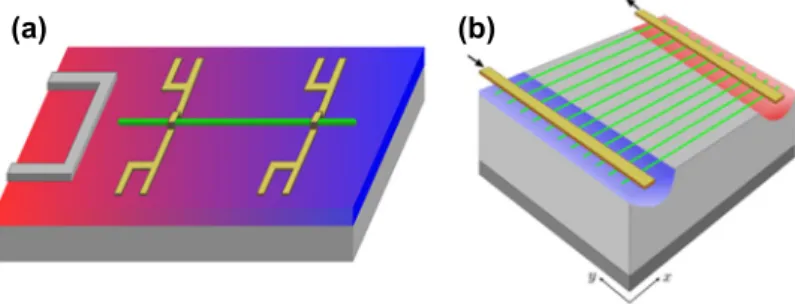
(a) (b)
Figure 1.NW-based MOSFETs: (a) A single NW (green) is deposited on an insulating substrate (red and blue). The source and the drain are made of two metallic electrodes (yellow), while Joule heating from an extra electrode (left side) can induce a temperature difference between the NW extremities. Varying the voltageVg applied upon the back gate (grey), one can shift the NW conduction band and probe thermoelectric transport in the bulk of the band, around its edges or even outside the band. This set-up has been used in Ref. [12] for measuring the thermopower of individual Si and Ge/Si NWs as a function ofVgat room temperature. (b) Array of parallel NWs deposited on a substrate with a back gate. The blue and red spots illustrate local cooling and heating effects in the activated regime, discussed in Section4.
(FET) device configuration. A detailed experimental study of electron tunneling and interferences in 1D Si-doped GaAs MOSFETs can be found in Ref. [5], where the electrical conductanceG of 1µm long NWs at 35 mK is given as a function of the gate voltageVg. One can make [6] arrays of vertical NW-based FET, each of them having a uniform wrap-around gate. To grow millions of thin NWs per cm2is possible. This gave us the motivation to study the TEs in 1D MOSFETs, from cryogenic temperatures where electron transport remains coherent towards higher temperatures where transport becomes activated, as a function of the location of the Fermi potentialEF inside the NW conduction band. The considered set-ups are sketched in Figure1.
There are many highly cited works describing the thermoelectric perfor- mance of NWs made of different materials: rough silicon [4,7], bismuth [8], bismuth telluride, III-V semiconductors (InAs, GaAs, and InP) [9], wide band gap semiconductors (ZnO and GaN) [10]. These studies have essentially been done around room temperature, and are mainly focused on the study of the phononic contribution to the thermal conductance [4,7] or of the effect of channel openings occurring when one varies the widths of superlattice quasi-1D NWs [8,11]. Thermoelectric transport is often described using 1D Boltzmann equations [8–10], and the role of localised impurity states (important in weakly doped semiconductors) as well as the Anderson localisation of the states (impor- tant in the 1D-limit) are not taken into account in these studies.
In this short review, we describe the effect of 1D Anderson localisation upon 1D thermoelectric transport, as one varies the location of the Fermi potentialEF
inside the NW conduction band. For this purpose, we use a purely 1D model (1D Anderson model) where the energy dependence of the localisation length and of the density of states (DOS) is analytically known in the weak disorder
limit. Though it does not allow us to describe the effect of channel openings occuring as one varies the NW width as in Refs. [8,11], these studies describe thermoelectric transport in NWs where the one body states are localised. A low temperature elastic regime is considered where the conductance and the thermopower are, respectively, obtained from the Landauer and Mott formulas, followed by the study of an inelastic regime occurring at higher temperatures and characterised by phonon-activated hopping between localised states (Mott variable range hopping). In this activated regime, thermoelectric transport is not described using semi-classical Boltzmann equations, but from the numerical solution of the random resistor network (RRN) model introduced by Miller and Abrahams for describing inelastic activated transport.
2. Elastic thermoelectric transport
To model a gated NW, we have considered in Ref. [13] a chain ofNsites coupled to two electronic reservoirsL(left) andR(right), in equilibrium at temperature TL=T+δT[TR =T] and chemical potentialμL =EF+δμ[μR =EF]. The Hamiltonian of the chain reads
H= −t
N−1
i=1
c†ici+1+h.c.
+ N
i=1
(i +Vg)c†ici, (2)
whereci†andciare the creation and annihilation operators of one electron on site iandtis the hopping energy. The lattice spacinga=1, theiare (uncorrelated) random numbers uniformly distributed in the interval[−W/2,W/2].
iVgc†ici
describes the effect of an external gate. VaryingVg, one can probe thermoelectric transport either in the bulk of the NW conduction band, around its edges or even outside the band.
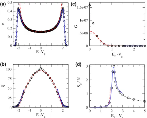
2.1. Typical thermopower
For the Hamiltonian (2), the dependence of the localisation lengthξ(E)and the DOS per siteν(E)on the energyEis analytically known [14] in the weak disorder limitW ≤ t. Within the band (|E−Vg| 1.5t),ξ(E)−1 can be expanded in integer powers ofWwhileν(E)remains well described by the DOS of the clean chain (W=0). This gives the bulk expressions
ξb(E)≈ 24 W2
4t2− |E−Vg|2
, νb(E)≈ 1
2πt
1−(|E−Vg|/2t)2. (3) WhenE−Vg approaches the band edges±2t, these expressions lead to diver- gences ofνandξ−1. As shown by Derrida and Gardner, these divergences are spurious and the correct expressions near the edges become
-2 -1 0 1 2 E -Vg
0 25 50 75 100
ξ
-2 -1 0 1 2
E -Vg 0
0,1 0,2 0,3 0,4 0,5
ν
(a)
(b) (d)
(c)
0 1 2
EF -Vg 0
5e-08 1e-07 1,5e-07
G
0 1 2 3 4 5
EF - Vg 0
1 2 3
S0 / N
Figure 2.1D Anderson model withW=t=1: (a) Density of states per siteν(E), (b) localisation lengthξ(E), (c) typical conductanceG(in units of 2e2/h), and (d) typical thermopowerS0(in units of(π2kB)/(3e)kBT).
Notes: In all panels, the red dashed line and the blue continuous line give the weak disorder behaviours in the bulk and near the edges (Equations (3–5) and (8–9)), while the black dashed line in (d) corresponds to Equation(10).
Circles are numerical results obtained forN=1600 ((a) and (b)) andN=800 ((c) and (d)).
ξe(E)=2 12t2 W2
1/3I−1(X)
I1(X) (4)
νe(E)= 2
π 12 tW2
1/3
I1(X)
[I−1(X)]2 (5) where
X=(|E−Vg| −2t)t1/3 12 W2
2/3
, In(X)= ∞
0
yn/2e−16y3+2Xydy. (6) The transmission coefficientT(E)of the disordered chain behaves typically as exp−2N/ξ(E). In the low temperature limitT →0, the electrical conductance G≈ 2eh2T(EF)while the thermopowerSis given by the Cutler-Mott formula,
S= π2kB2T
3|e|t S with S≈ −t d lnT dE
EF
. (7)
From the weak disorder expansions of ξ(E), one can deduce the typical dimensionless thermopower S0 (thermopower in units of (π2k2BT)/(3|e|t)).
This gives, respectively in the bulk of the band (superscriptb) and at its edges (superscripte):
S0b =N (EF−Vg)W2
96t3[1−((EF−Vg)/2t)2]2, (8) S0e=2N 12t2
W2 1/3
I3(X) I−1(X)−
I1(X) I−1(X)
2
, (9)
whereX=X(E=EF). Outside the band, one estimates the typical thermopower by assuming that the system behaves as a clean tunnel barrier (superscriptTB).
One obtains S0TB
N ≈
N→∞ −1
N 2t (EF)
d dE
EF
∓ 1
E
F−Vg 2t
2
−1
(10)
with a + sign whenEF ≤ Vg −2t and a− sign whenEF ≥ Vg +2t. Here (E) = i[(E)−†(E)] where(E)is the self-energy of the (identical) left and right leads, evaluated at the sites located at the chain extremities to which the leads are attached. In Figure2, one can see that the analytical weak disorder expressions of the DOS per site ν(E), of the localisation length ξ(E), of the electrical conductanceG(E)and of the typical thermopowerS0(E)(in units of (π2k2BT)/(3|e|t)) describe accurately numerical results (for more details, see Ref.
[13]), even if they are computed for a relatively large disorder (W=t).
2.2. Mesoscopic fluctuations
In the elastic localised regime, the sample-to-sample fluctuations of the dimen- sionless thermopowerSaround its typical valuesS0borS0eturn out to be large. If EF =Vg,S0=0 due to particle-hole symmetry but the mesoscopic fluctuations allow for a largeS anyway. Assuming Poisson statistics for the energy levels, Van Langen et al. showed in Ref. [15] that the thermopower distribution is a Lorentzian whenN ξ,
P(S)= 1 π
2+(S−S0)2. (11) The width=2πt/Fis given by the mean level spacingF =1/(Nν(EF))at the Fermi energyEF. Van Langen et al. assumedS0 =0, an assumption which is only correct at the band centre. We have calculatedP(S)using recursive Green function method for different values ofVg and have numerically checked [13]
that Equation (11) describes also P(S) if one takes forS0 the value given by Equations (8) or (9) instead ofS0 = 0. As one crosses the band edges, we have numerically observed a sharp crossover towards a Gaussian distribution
P(S)= 1
√2πλexp
−(S−S0)2 2λ2
, (12)
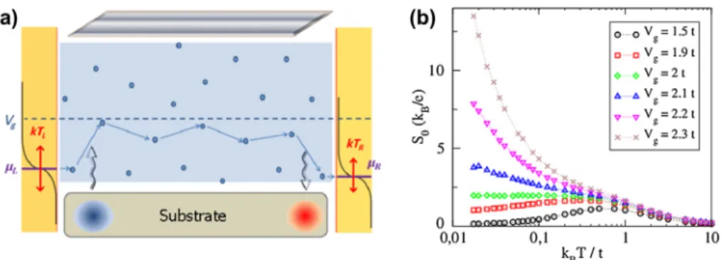
Figure 3.(a) The electronic localised states (blue dots) are randomly located along the chain within an energy band of width 4t+W(shaded light blue region). In the left and right reservoirs, the electrons are at equilibrium with Fermi–Dirac distributions of temperaturesTL = T +δT, TR =Tand electrochemical potentialsμL =EF+δμ,μR=EF. Varying the voltageVgapplied to the gate (top grey region) shifts the NW conduction band, making possible to probe electron transport inside the band, around its edges or outside the band. The electrons can hop between states of different energies by absorbing or emitting a phonon. For a NW deposited on a substrate, the phonons are provided by the substrate and characterised by a Bose–Einstein distribution of temperatureTS(TS=Tthroughout the paper, except in Section5). Electrons injected near the lower band edge mainly find available states to jump to at higher energies near the source (left reservoir). This implies that the phonons are mainly absorbed from the substrate near the source (blue region), and emitted back to the substrate near the drain (red region), as indicated by the two arrows. (b) Typical thermopowerS0(in units ofkB/e) as a function ofkBT/t, calculated for a chain of lengthL=200 (EF=0 andW=t) for increasing values ofVg.
where the typical valueS0 is given by Equation (10) and the widthλincreases linearly with√
NandW. In Ref. [13], one can find numerical results which are perfectly described by the above analytical expressions whenW=t.
3. Inelastic thermoelectric transport
When one increases the temperature T, electron transport becomes mainly inelastic and activated. The inelastic effects can be due to electron–electron, electron–photon and electron–phonon interactions. Electron–electron interac- tions in a many-electron system with localised single-particle states can in- duce a metal-to-insulator transition above a certain critical temperature [16].
These interactions can also induce the Coulomb-gap behaviour [17] observed in δ-dopedGaAs/AlxGa1−xAs2D heterostructures at low temperature [18], provid- ing evidence of possible phononless hopping. Electron–photon interactions are responsible for the photovoltaic effects. In Ref. [20], we have studied the variable range hopping (VRH) regime introduced by Mott [21] where electron–phonon coupling dominates. Figure3(a) illustrates how electrons propagate through the NW in the Mott VRH regime.
3.1. Variable range hopping
In the VRH regime, the electrons propagate by hopping from one localised state to another, of higher energy by absorbing a phonon or of lower energy by emitting
a phonon. Let us summarise Mott’s original argument [21]. The electron transfer from a statei to another statejseparated by a distanceLij in space andijin energy results from a competition between the probability ∝ exp−(Lij/ξ)to tunnel over a length Lij and the probability ∝ exp−ij/(kBT) to change the electron energy by an amount ij = 1/(νLij), where ν is the DOS per site.
These estimates neglect the energy dependence ofξandνaroundEF. In 1D, the optimal hopping length is given by theMott length LM (ξ/2νkBT)1/2, if the localisation lengthsξ and DOS per unit lengthν do not vary within the Mott energy window M = 1/(νLM) = kB√
TTM around EF.LM decreases as the temperature increases. One defines the activation temperaturekBTx ξ/(2νL2) at whichLM Land the Mott temperaturekBTM 2/(νξ)at whichLM ξ. The inelastic VRH regime corresponds toTx < T < TM where the electrical conductance
G∝exp−(2LM/ξ)∝exp−(M/kBT). (13) Below Tx elastic tunneling dominates, whileLM < ξ aboveTM and transport becomes simply activated. In 1D, the crossover from VRH to simply activated transport takes even place [22,23] at a temperatureTalower thanTM. The reason is the presence of highly resistive regions in energy-position space, where 1D electrons cannot find empty states at distances∼M,LM.
3.2. Random resistor network with energy-dependent localisation length and DOS
If the variation ofξ(E)andν(E)as a function of the energyEis not negligible within the characteristic scaleM, we need to go beyond this simple argument, notably around the 1D band edges. We use a simplified model where the energies Eiof the localised states areNuncorrelated variables of probability given by the DOSν(E)of the 1-D Anderson model for a chain of lengthL = Na(a = 1), while theNlocalisation lengthsξ(Ei)are given by the typical values of this model (Equations (3) and (4)). TheNpositionsxiare taken at random in the interval [0,L]. As in Refs. [24,25], we solve the corresponding Miller–Abrahams RRN [26] made of all possible links connecting theN nodes given by theNlocalised states. Each pair of nodesi,jis connected by an effective resistor, which depends on the transition rates ij, ji induced by local electron–phonon interactions.
For a pair of localised statesiandjof energiesEiandEj, Fermi golden rule [25]
gives:
ij=γijfi(1−fj)
Nij+θ(Ei−Ej)
, (14)
wherefiis the occupation number of stateiandNij = [exp{|Ej−Ei|/ kBT}−1]−1 is the phonon Bose distribution at energy |Ej − Ei|. The Heaviside function accounts for the difference between phonon absorption and emission [19].γijis the hopping probabilityi →jdue to the absorption/emission of a phonon when
iis occupied andjis empty. It is given by γij
1/ξi−1/ξj
2
γep = exp{−2xij/ξj}
ξi2 +exp{−2xij/ξi}
ξj2 −2 exp{−xij(1/ξi+1/ξj)}
ξiξj
(15) wherexij= |xi−xj|andγepdepends on the electron–phonon coupling strength and of the phonon DOS. If the energy dependence ofξ andνcan be neglected withinM, one recovers the usual limitγij γepexp(−2xij/ξ).
The direct transition rates between each state i and the contacts α (source α =Land drainα =R) are assumed to be dominated by elastic tunneling (see Refs. [24,25]) and read
iα =γe,αexp(−2xiα/ξi)fi
1−fα(Ei)
. (16)
fα(E)= [exp{(E−μα)/kBT} +1]−1is the contactα’s Fermi–Dirac distribution, xiα denotes the distance of the stateifromα, andγe,α is a rate quantifying the coupling between the localised states and the contact α. The electric currents flowing between each pair of states and between states and contacts read
Iij=e( ij− ji), (17a)
Iiα=e( iα− αi), α =L,R. (17b) e < 0 is the electron charge. Hereafter, we will take γep = t/and symmetric couplingsγe,L=γe,R =t/.
For solving the RRN, we consider it at equilibrium with a temperatureTand a chemical potentialμ=EFeverywhere. A small electric currentIecan be driven by adding to the left contact (the source) a small increase δμ of its chemical potential (Peltier configuration). If δμ is sufficiently small, one has Ie ∝ δμ (linear response). At equilibrium (δμ = 0), the N occupation numbersfi are given by Fermi–Dirac distributionsfi0 = (exp[(Ei −EF)/kBT] +1)−1. When μL→EF+δμ,fi →fi0+δfi. For having the currentsIijandIiα, we only need to calculate theNchangesδfi induced byδμ =0. Imposing current conservation at each node i of the network (
jIij +
αIiα = 0) and neglecting terms
∝ δfi.δfj (linear response), one obtainedN coupled linear equations. Solving numerically this set of equations gives theNchangesδfiand hence all the currents IijandIiα. From this, we can calculate the total chargeILe = −
iIiLand heat IL(R)Q =
i(Ei−μL(R))/e)IiL(R)currents, and hence the electrical conductance G, the Peltier coefficientand the Seebeck coefficientSin the VRH regime.
G= ILe
δμ/e, = ILQ
ILe, S= 1 T
ILQ
ILe. (18)
In the last equation, the Kelvin–Onsager relation = ST has been used for obtaining the thermopowerSfrom the Peltier coefficient.
3.3. Activated thermoelectric transport in arrays of parallel NWs
Using the 1D weak-disorder expressions (Equations (3)–(5)) forν(E)andξ(E), we have studied activated transport throughN localised states of energyEi and localisation lengthξ(Ei). The states were assumed to be randomly located along a chain of length L = Na, and the energies Ei were taken at random with a probability ν(E) inside an energy band [−2, 2] where = t +W/4. The corresponding thermopower distributionsP(S)are given and discussed in Ref.
[20]. We reproduce in Figure 3(b) the curves giving the typical thermopower S0(in units ofkB/e) as a function ofkBT/t for increasing values ofVg. Taking EF = 0,S0 has been calculated for a chain of length L = 200 with W = t.
Vg = 0 corresponds to the band centre andVg/t = ±2.5 to the band edges.
WhenkBT < t,S0 remains small within the band (Vg ≈ 1.5t), but becomes much larger around its edges (Vg =2.3t). At higher temperatures,S0decreases and becomes independent ofVg. If activated transport at the band edges give rise to large thermopowers, it is also characterised by small electrical conductances, which defavour large values for the power factors Q. This led us to consider in Ref. [27] arrays of parallel nanowires in the field-effect transistor device configuration. In such arrays, the conductances add while the thermopower fluctuations self-average. The maximal output powerPmax=Q(δT)2/4 is found to be maximal near the band edges, while the electronic figure of merit (obtained without including the phononic contributionKph to the thermal conductance) keeps a large value ZeT ≈ 3. As estimated in Ref. [27], Pmax can be of the order ofPmax ≈ 20γ˜eµW forM = 105parallel silicon NWs withδT ≈ 10 K, T ≈100 K, andt/kB ≈150 K. The larger isMorδT, the larger isPmax. Estimates of the constant γ˜e = γe/t give values≈ 0.01−1. If one takes into account Kph, we expect thatZT ≈ ZeT/(1+2/γ˜e)for Silicon suspended NWs, while ZT ≈ZeT/(1+20/γ˜e)for Silicon NWs deposited on a Silicon Dioxide substrate.
4. Using electron–phonon coupling for managing heat
The phonons have no charge and cannot be manipulated with bias and gate voltages, in contrast to electrons. This makes difficult to manage heat over small scales, unless we take advantage of the electron–phonon coupling for transferring heat from the phonons towards the electrons. Let us show how this can be done using phonon-activated transport near the edges of a NW conduction band.
We take a NW deposited on a substrate with a back gate, and assume that the transport of NW-electrons is activated mainly because of the substrate phonons.
Let us consider a pair of localised statesiandj. The heat current absorbed from (or released to) the substrate phonon bath by an electron hopping fromi toj readsIijQ =
Ej−Ei
IijN, whereIijN = ij− jiis the hopping particle current betweeni andj. The local heat current associated with the statei is given by summing over the hops fromito all the statesj:
(a)
(c) (d)
(b)
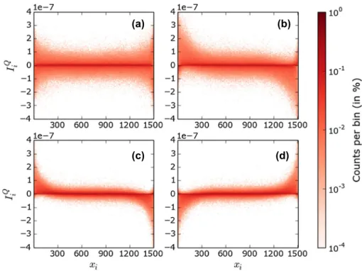
Figure 4.2D histograms giving the distribution of local heat currentsIiQ (Equation(19)) as a function of the positionxialong the NW, for four values of the gate potential: (a)Vg = 0, (b) Vg=t, (c)Vg=2.25t, and (d)Vg= −2.25t.
Note: Parameters:L=1500,W=t,kBT=0.5t,δμ=10−5t, statistics over 500 NWs.
IiQ=
j
IijQ=
j
Ej−Ei
IijN. (19)
In Figure4, we show 2D histograms of the local heat currentsIiQas a function of the positionxi of the stateiinside the NW. We take the convention thatIiQ is positive (negative) when the phonons are absorbed (emitted), thus heating (cooling) the electrons at site i. We have numerically solved the RRN (see Subsection 3.2) for a temperature kBT = 0.5 t, W = t and four different values ofVg, corresponding to electron injection at the band centre (Vg = 0), below the band centre (Vg =t) and around the lower (Vg =2.25t) and upper (Vg = −2.25t) band edges of the NW conduction band. At the band centre, the fluctuations of the local heat currents are symmetric around a zero average. They are larger near the NW boundaries and remain independent of the coordinate xi otherwise. Away from the band centre, one can see that the fluctuations are no longer symmetric near the NW boundaries, though they become symmetric again far from the boundaries. When the electrons are injected through the NW in the lower energy part of the NW band, more phonons of the substrate are absorbed than emitted near the source electrode. The effect is reversed when the electrons are injected in the higher energy part of the band (by taking a negative gate potentialVg): It is now near the drain that the phonons are mainly absorbed.
The 2D histograms corresponding toVg =2.25tand−2.25tare symmetric by inversion with respect toIiQ =0.
As explained in Refs. [27,28], activated transport near the band edges of disordered NWs opens interesting ways for managing heat at small scales, notably for cooling hot spots in microprocessors. TakingM = 2.105 NWs contacting two 1−cm long electrodes, one estimates that we could transfer 0.15 mW from the source side towards the drain side by takingδμ/e ≈ 1 mV at T = 77 K.
Again, the larger isMorδμ, the larger is the heat of the substrate which can be transfered from the source towards the drain by hot electrons.
5. Activated multi-terminal thermoelectric transport and ratchet effects In Sections 3and 4, we have discussed activated transport in a configuration where the source, drain and substrate were at the same equilibrium temperature T, the heat and particle currents between the source and the drain being induced by a small voltage biasδμand/or temperature biasδT. More generally, a disor- dered NW deposited on a substrate can be viewed as the three-terminal set-up sketched in Figure5(a): Two electronic reservoirsL(source) andR (drain) at equilibrium with electrochemical potentials μL,μR, and temperaturesTL,TR, while the substrate provides a third reservoirSof phonons at a temperatureTS. Heat and particles can be exchanged betweenLandR, but only heat withS. The particle currentsILN,IRN, and the heat currentsILQ,IRQ,ISQare taken positive when they enter the NW from the three reservoirs. The drain is chosen as reference (μR ≡EF andTR ≡ T) and we setδμ =μL−μR,δT =TL−TR, andδTS = TS−TR. In linear response the charge and heat currentsILN,ILQ, and the heat currentISQcan be expressed à la Onsager in terms of the corresponding driving
forces ⎛
⎜⎝ ILN ILQ ISQ
⎞
⎟⎠=
⎛
⎝L11L12L13
L12L22L23
L13L23L33
⎞
⎠
⎛
⎝ δμ/T δT/T2 δTS/T2
⎞
⎠ . (20)
The Casimir–Onsager relationsLij=Ljifori=jare valid in the absence of time- reversal symmetry breaking. In Ref. [29], we have discussed several possibilities offered by this set-up whenδTS=0, in terms of energy harvesting and cooling.
Let us focus on the case where the NW is deposited on a hotter substrate without bias and temperature difference between the source and the drain (δμ =δT = 0 while δTS > 0). If the particle-hole symmetry and the left–right inversion symmetry are broken, the heat provided by the phonons can be exploited to produce electrical work. Let us consider a model where the NW localised states are uniformly distributed in space and energy within a band [−2, 2] with a constant DOS ν = 1/(4) and an energy independent localisation length ξ = 4. We have solved the corresponding RRN for an ensemble ofM parallel NWs with asymmetric elastic couplings to the electronics reservoirs. In average over an ensemble of M NWs, particle-hole symmetry is broken if the Fermi
(a) (b)
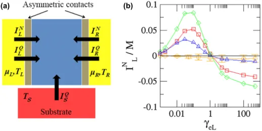
Figure 5.(a): Scheme of the three-terminal set-up corresponding to activated thermoelectric transport for a NW deposited on a substrate. The NW (blue) is connected to two electronic electrodes (yellow)L(the source) andR(the drain) via asymmetric contacts. The electrodes are at equilibrium (electrochemical potentialsμL,μR, and temperaturesTL,TR). The insulating substrate (red) provides a phonon bath of temperatureTS. (b): Ratchet effect powered byδTS = 10−3 whenδT = δμ = 0. For various values ofVg(Vg/ = 0 ( ), 0.5 ( ), 1 ( ) and 2.5 ( )), the average particle currentsILN/M(in unit of 105/) of an array ofM=2.105parallel NWs is given as one variesγeL (elastic coupling to the source), keeping the same valueγeR = /for the elastic coupling to the drain.ILN/M =0, unlessVg =0 (particle-hole symmetry) orγeL = γeR
(inversion symmetry).
potentialEF ≡ 0 does not coincide with the NW band centre (Vg = 0), and inversion symmetry is broken by taking different elastic coupling constants in Equation (16) (γe,L=γe,R). Figure5(b) gives the average particle currentILN/M between the source and the drain as a function ofγe,Lwhenγe,R =1 (in units of/).ILN/M was induced by a temperature differenceδTS =10−3between the substrate and a deposited array ofM = 2.105 parallel NWs. One can see thatILN ≈ 0 at the band centre (Vg = 0) and whenγe,L = γe,R, whileILN = 0 otherwise. Other ways of breaking inversion symmetry which give rise to even larger currentsILN are discussed in Ref. [29].
6. Conclusion
Our studies were restricted to the elastic tunnel regime and to the Mott VRH regime where electron–phonon interactions dominate. We have considered arrays of parallel purely 1D NWs where the electron states are localised and neglected the effects of electron–electron and electron–photon interactions. In bulk 3D amorphous germanium, silicon, carbon and vanadium oxide [19], the Mott VRH behaviour was observed in a temperature range 60K < T <
300K. This shows us that Mott VRH is relevant in a broad temperature domain which can reach room temperature. At lower temperatures, Efros–Shklovskii hopping behaviour was observed in 2D heterostructures [18] with a universal
prefactor, indicating that the effects of electron–electron interactions become more relevant than these of electron–phonon interactions as one decreases the temperature [30]. Eventually, let us note that in bulk weakly-doped crystalline semiconductors, the electrons can be activated from the impurity band up to the conduction band when the temperature exceeds the energy gap between these two bands, putting an upper limit to VRH transport. The width of this energy gap can vary from one material to another. This is what can be said for bulk 3D or 2D materials. To extend these conclusions to 1D NWs is not straightforward, since the effect of disorder (Anderson localisation) and of electron–electron interactions (Wigner glass) is much more relevant in the 1D limit. Moreover, the temperature range where our predictions apply can vary from one semiconductor to another, and can depend on the width of the NWs.
In summary, we have shown that arrays of 1D MOSFETs have good ther- moelectric performances, notably when the electrochemical potential is in the vicinity of the NW band edges. The described effects could provide an interesting method for converting waste heat into useful electrical power and for cooling hot spots in microprocessors. Ratchet effects open interesting perspectives when electrical transport in deposited NWs can be activated by the phonons of the sub- strate. The studied devices are based on standard nanofabrication technologies which are widely developed in semiconductor microelectronics.
Disclosure statement
No potential conflict of interest was reported by the authors.
References
[1] E. Pop, S. Sinha and K. Goodson, Proc. IEEE. 94 (2006) p.1587.
doi:10.1109/jPROC.2006.879794
[2] A.F. Ioffe, Semiconductor Thermoelements, and Thermoelectric Cooling, Infosearch Limited, London,1957.
[3] H.J. Goldsmid,Introduction to Thermoelectricity, Springer-Verlag, Berlin Heidelberg, 2010.
[4] A.I. Hochbaum, R. Chen, R.D. Delgado, W. Liang, E.C. Garnett, M. Najarian, A.
Majumdar and P. Yang, Nature 451 (2008) p.163. doi:10.1038/nature06381 [5] W. Poirier, D. Mailly and M. Sanquer, Phys. Rev. B 59 (1999) p.10856.
[6] C. Thelander, P. Agarwal, S. Brongersma, J. Eymery, L.F. Feiner, A. Forchel, M. Scheffler, W. Riess, B.J. Ohlsson, U. Gsele and L. Samuelson, Mater. Today 9 (2006) p.28.
[7] A.I. Boukai, Y. Bunimovich, J. Tahir-Kheli, W.A. Goddard III and J.R. Heath, Nature 451 (2008) p.168. doi:10.1038/nature06458
[8] X. Sun, Z. Zhang and M.S. Dresselhaus, Appl. Phys. Lett. 74 (1999) p.4005.
doi:10.1063/1.123242
[9] N. Mingo, Appl. Phys. Lett. 84 (2004) p.2652. doi:10.1063/1.1695629
[10] C.-H. Lee, G.-C. Yi, Y. Zuev and P. Kim, Appl. Phys. Lett. 94 (2009) p.022106.
doi:10.63/1.3067868
[11] Y.-M. Lin, X. Sun and M.S. Dresselhaus, Phys. Rev. B 62 (2000) p.4610.
[12] Y.U. Brovman, J.P. Small, Y. Hu, Y. Fang, C.M. Lieber and P. Kim, J. Appl. Phys. 119 (2016) p.234304. doi:10.1063/1.4953818
[13] R. Bosisio, G. Fleury and J.-L. Pichard, New J. Phys. 16 (2014) p.035004.
doi:10.1088/1367-2630/16/3/035004
[14] B. Derrida and E. Gardner, J. Phys. Fr. 45 (1984) p.1283.
[15] S.A. van Langen, P.G. Silvestrov and C.W.J. Beenakker, Supperlattices Microstruct. 23 (1998) p.691.
[16] D.M. Basko, I.L. Aleiner and B.L. Altshuler, Ann. Phys. 321 (2006) p.1126.
doi:10.1016/j.aop.2005.11.014
[17] B.I. Shklovskii and A.L. Efros,Electronic Properties of Doped Semiconductors, Springer, Berlin,1984.
[18] S.I. Khondaker, I.S. Shlimak, J.T. Nicholls, M. Pepper and D.A. Ritchie, Phys. Rev. B 59 (1999) p.4580.
[19] V. Ambegaokar, B.I. Halperin and J.S. Langer, Phys. Rev. B 4 (1970) p.2612.
[20] R. Bosisio, C. Gorini, G. Fleury and J.-L. Pichard, New J. Phys. 16 (2014) p.095005.
doi:10.1088/1367-2630/16/9/095005
[21] N.F. Mott and E.A. Davies,Electronic Processes in Non Crystalline Materials2nd ed., Clarendon, Oxford,1979.
[22] J. Kurkijarvi, Phys. Rev B 8 (1973) p.922.
[23] M.E. Raikh and M.E. Ruzin, Sov. Phys. JETP 68 (1989) p.642.
[24] J.H. Yiang, O. Entin-Wohlman and Y. Imry, Phys. Rev. B 85 (2012) p.075412.
[25] J.H. Yiang, O. Entin-Wohlman and Y. Imry, Phys. Rev. B 87 (2013) p.205420.
[26] A. Miller and E. Abrahams, Phys. Rev. 120 (1960) p.745.
[27] R. Bosisio, C. Gorini, G. Fleury and J.-L. Pichard, Phys. Rev. Appl. 3 (2015) p.054002.
doi:10.1103/PhysRevApplied.3.054002
[28] R. Bosisio, C. Gorini, G. Fleury and J.-L. Pichard, Phys. E 74 (2015) p.340.
doi:10.1016/j.physe2015.07012
[29] R. Bosisio, G. Fleury, J.-L. Pichard and C. Gorini, Phys. Rev. B 93 (2016) p.165404.
doi:10.1103/PhysRevB.93.165404
[30] L. Fleishman, D.C. Licciardello and P.W. Anderson, Phys. Rev. Lett. 40 (1978) p.1340.
doi:10.1103/PhysRevLett.40.1340