Feature Article
basic solid state physics
Interplay of Rashba/Dresselhaus spin splittings probed by photogalvanic spectroscopy – A review
Sergey D. Ganichev*,1and Leonid E. Golub2
1University of Regensburg, 93040 Regensburg, Germany
2Ioffe Physical-Technical Institute of the RAS, 194021 St. Petersburg, Russia Received 9 October 2013, revised 15 February 2014, accepted 20 February 2014 Published online 22 March 2014
Keywords photogalvanics, Rashba/Dresselhaus spin splittings, semiconductors
∗Corresponding author: e-mailsergey.ganichev@ur.de, Phone:+49 941 9432050, Fax:+49 941 9431657
This is an open access article under the terms of the Creative Commons Attribution License, which permits use, distribution and reproduction in any medium, provided the original work is properly cited.
The paper reviews the interplay of Rashba/Dresselhaus spin splittings in various two-dimensional systems made of zinc- blende III–V, wurtzite, and SiGe semiconductors. We discuss the symmetry aspects of the linear and cubic in electron wavevector spin splitting in heterostructures prepared on (001)-, (110)-, (111)-, (113)-, (112)-, and (013)- oriented substrates and address the requirements for suppression of spin relaxation
and realization of the persistent spin helix state. In experi- mental part of the paper, we overview experimental results on the interplay of Rashba/Dresselhaus spin splittings probed by photogalvanic spectroscopy: The method based on the phe- nomenological equivalence of the linear-in-wavevector spin splitting and several photogalvanic phenomena.
1 Introduction Quantum phenomena in semiconduc- tors are highly sensitive to subtle details of the carrier energy spectrum so that even a small spin splitting of energy bands may result in measurable effects. A textbook example of the band spin splitting is the Zeeman effect, which is caused by the coupling of an external magnetic field and electron spin.
However, band spin degeneracy can also be removed with- out action of a magnetic field. This phenomenon is caused by the spin–orbit interaction (SOI) in noncentrosymmetric crystals, a relativistic effect allowing for coupling of elec- tron spin and orbital degrees of freedom. As a result the spin degeneracy of the energy bands is lifted even in nonmagnetic materials. This coupling is described by a Hamiltonian with products ofσandkterms whereσare the Pauli spin matri- ces andk is the electron wave vector. The origin of these terms are the bulk inversion asymmetry (BIA) and the struc- ture inversion asymmetry (SIA). Microscopically, BIA stems from the absence of the inversion symmetry in the bulk mate- rial and gives rise to the Dresselhaus spin splitting in bulk and low-dimensional semiconductors [1, 2]. By contrast, SIA originates from the inversion asymmetry of the confining potential and yields the Rashba term in the Hamiltonian
whose strength can be manipulated by an external elec- tric field (Rashba effect) [3, 4]. In particular, the SIA/BIA coupling of the electron wavevector and spin causes a Lar- mor precession in an internalk-dependent effective magnetic field for electrons moving through a semiconductor structure.
Note that in addition to BIA and SIA, an interface inver- sion asymmetry (IIA) may yield k-linear terms caused by noninversion symmetric bonding of atoms at heterostructure interfaces [5–7]. Since the IIA results in the SOI of the same form as BIA in (001)-grown III–V systems, we disregard this type of spin splitting in further consideration.
While the existence of the zero-magnetic field spin split- ting is known since the 1960s of the last century [1, 3], it quickens an enormous interest since manipulation of the electron spin instead of its charge has been considered as a candidate for the future electronics – spintronics. The cause of this interest is that the Rashba effect in two-dimensional electron systems (2DES) provides a unique possibility to manipulate electron spin by means of external electric field and is of great importance for the generation, manipulation, and detection of spin currents as well as for control of the spin relaxation processes in low-dimensional semiconductors, for
by means of electric field, pure spin currents, and electric currents caused by spin polarization have attracted contin- uously growing interest from both the experimental and theoretical points of view. Most of these works are aimed to two-dimensional systems, where BIA and SIA terms cou- ple thein-planewavevector of confined electronskwith the in-orout-of-planecomponents of the electron spinS. The relative orientation of the coupled k- andS-components is determined by the symmetry of the system. Consequently, it depends on the QW growth plane crystallographic orientation and on the considered direction of the in-plane wavevector. In many systems, the SIA and BIA terms can interfere resulting in an anisotropy of the spin splitting. The strongest anisotropy can be achieved in (001)-grown quantum wells (QWs) with the k-linear Rashba and Dresselhaus terms of equal strength. Under these circumstances, the dominant mecha- nism of spin dephasing (Dyakonov–Perel relaxation [20]) is suppressed [21–23] making possible a diffusive spin field transistor [24] as well as giving rise to a persistent spin helix (PSH) predicted in Ref. [25] and observed in GaAs low- dimensional systems [26, 27]. In fact, for this particular case, the spin splitting vanishes in certaink-space directions and an effective magnetic field caused by SOI is aligned along a cer- tain crystallographic axis for allkbeing ineffective for spins oriented along this axis, see, e.g., Refs. [22, 24, 28]. Further important example of the SIA/BIA anisotropy is manipula- tion of the spin dephasing in QWs grown on (110) or (111) crystallographic planes where extremely long spin relaxation times have been experimentally achieved by adjusting of Rashba and Dresselhaus spin splitting [29–42]. Lately, there has been much effort in the studying of the SIA/BIA-interplay both theoretically with new device proposals [24, 43–46]
and experimentally with the aim to obtain particular rela- tion between SIA and BIA spin splitting in QW systems of various crystallographic orientations.
Owing to the fact that Rashba/Dresselhaus zero magnetic field spin splittings give rise to a large number of diverse physical phenomena their characterization and control are of fundamental importance for spin physics in semiconduc- tors. The relative orientation of spin and electron wavevector in eigenstates and strength of these splittings depend on macroscopic conditions such as structure crystallographic orientation, QW width, temperature, electron density, dop- ing profile, stress, etc. Consequently, the interplay of the Rashba/Dresselhaus spin splittings is strongly affected by these parameters and requires a detailed study. Various methods providing an experimental access to the SIA/BIA interplay have been developed to which belong (i) inves- tigations of the anisotropy of the Raman effect [47, 48];
(ii) study of the weak antilocalization (WAL) [49–53]
and WAL in tilted magnetic fields [54–57]; (iii) photogal- vanic effects [33, 58–66]; (iv) investigation of spin-relaxation anisotropy by Hanle-effect [67]; (v) study of the gate depen- dence of spin relaxation [68–71], as well as (vi) experiments on time resolved Kerr effect (TRKR) or Faraday rotation in special experimental geometries [72–79], including magne-
optical monitoring the angular dependence of the electron spin precession on their direction of motion with respect to the crystal lattice [75]. The multifaceted SIA/BIA spin splitting has been the subject of a tremendous number of works and numerous reviews. Our contribution to this special issue is primary focused on the results obtained in the frame- work within the DFG Schwerpunktprogramm SPP 1285 and, consequently, limited to the investigation of SIA/BIA explored by study of the photogalvanic effects anisotropy.
The developed methods are based on the phenomenological equivalence of SIA/BIA spin splitting and several photo- galvanic phenomena [28, 80, 81], which all have a common property: They are described by the linear coupling of a polar vector and an axial vector, like the electron wavevector with its spin in Rashba/Dresselhaus effect or, e.g., electric current with an average nonequilibrium spin in the spin- galvanic effect [58]. Indeed, such phenomena are described by second rank pseudo-tensors whose irreducible compo- nents differ by a scalar factor only. Therefore, these methods allow determination of the spin–orbit coupling anisotropy in 2DES and do not require a knowledge of microscopic details or rely on theoretical quantities. Furthermore, previ- ous studies demonstrated that the discussed effects are very general and measurable signals can be obtained for almost all 2DES and even at room temperature, for reviews see, e.g., Ref. [80]. Thus, photogalvanic experiments allow us characterization of the SIA/BIA interplay upon variation of macroscopic parameters in a wide range.
The paper is organized in the following way: In Sec- tion 2, an overview of the symmetry aspects of the Rashba/Dresselhaus effects in III–V semiconductor mate- rials is given. First the removal of spin degeneracy due to spin–orbit interaction is addressed and then the SIA/BIA spin splitting ink-space for 2DES grown in various crystal- lographic directions is presented. Sections 3 and 4 introduce the method based on photogalvanics and give a short account for the experimental technique, respectively. The experimen- tal results on interplay of SIA/BIA upon variation of 2DES design and characteristics are presented and discussed in Sec- tions 5 (zinc-blende III-V-based QWs), 6.1 (wurtzite 2DES), and 6.2 (SiGe QWs). Conclusions and outlook are given in Section 7.
2 Symmetry analysis of the Rashba/Dresselhaus band spin splitting in zinc-blende materials In the absence of external magnetic fields, the time inversion results in the Kramers theorem which reads as ε↑(k)=ε↓(−k).
Here,εis electron energy, and↑/↓enumerate two spin states.
If the system has an inversion center then, applying the space inversion operation, one getsε↑(k)=ε↑(−k). Com- bining these two results, we see that two spin states with the same wavevectorkhave the same energy and the elec- tron energy spectrum close to the conduction band minima is well described by a parabolic dispersion:ε↑(k)=ε↓(k)= 2k2/(2m∗), wherem∗is the effective mass in the conduction band.
Table 1 Correspondence between growth-orientation dependent x, y, zlabels and crystallografic orientations. Note that in (001)- grown III–V material-based QWs in a valuable number of works aimed to SIA/BIA spin splitting cubic axes with x[100] and y[010] are used.
growth plane
zinc-blende and SiGe wurtzite
bulk (001) (110) (111) (113)
x [100] [1¯10] [¯110] [11¯2] [1¯10] [11¯20]
y [010] [110] [001] [¯110] [33¯2] [1¯100]
z [001] [001] [110] [111] [113] [0001]
However, in the system lacking an inversion center, e.g., zinc-blende and wurtzite bulk semiconductors and 2DES, the spin splitting can be present even in zero magnetic field. Such a splitting is caused by SOI. The corresponding Hamiltonian HSOis given by a sum of products of the Pauli matrices and odd combinations of the wavevector components. In bulk III–
V semiconductors belonging toTdpoint group symmetry it is described by the cubic in the wavevectorkterms introduced by Dresselhaus [1]:
Hbulk=γ[σxkx(ky2−kz2)+σyky(k2z−k2x)
+σzkz(k2x−k2y)]. (1) Here,γis the only one linearly-independent constant for the Td point group and x, y, z are cubic axes. Note that here- after the crystallographic orientation ofx, y, zaxes for each considered system is given in Table 1. Despite this splitting determines the Dyakonov–Perel spin relaxation rate, its value can not be manipulated by an electric field and is determined by the constantγ.
In 2D systems, confinement and symmetry lowering result in a more rich SOI, which is described by new terms in the Hamiltonian both, linear and cubic, in the electron 2D wavevector. The corresponding spin–orbit splitting is sensi- tive to external parameters like electric field, temperature, structure design, crystallographic orientation, etc. Below we consider one by one QW structures grown in various direc- tions. The three point groups D2d, C2v, and Csare particularly relevant for zinc-blende structure-based QWs [28, 82, 83].
Hereafter, the Sch¨onflies notation is used to label the point groups. In the international notation, they are labeled as ¯42m, mm2, andm, respectively.
2.1 Rashba/Dresselhaus terms in (001)-grown zinc-blende structure-based 2DES Quantum well structures made of III–V semiconductors MBE grown on (001)-oriented substrates are the most studied low- dimensional systems. The point symmetry group of these structures can be either D2d or C2v which both belong the gyrotropic point groups [84] and, consequently allow linear in wavevector spin splitting. TheD2dsymmetry corresponds to (001)-oriented symmetrical QWs. In such QWs, only BIA terms may exist. If an additional up-down asymmetry is
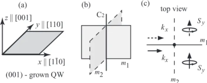
Figure 1 (a) Coordinate system used for (001)-grown III–V QWs, (b) symmetry elements of the C2vpoint group: mirror planesm1and m2and C2-axis in the QW grown alongz [001]. Arrows in the drawing (c) show that the reflection in the mirror planem1does not change the sign of both the polar vector componentkxand the axial vector componentSy, demonstrating that a linear coupling between kxandSyis allowed under this symmetry operation. This coupling is also allowed by the other symmetry operations (mirror reflection by the planem2 at which both components change their sign and the C2 rotation axis) of the point group yielding thekxσyterms in the effective Hamiltonian.
present due to, e.g., nonequivalent interfaces, asymmetric doping, or electric field applied normally to QW plane, then the symmetry is reduced to C2vgiving rise to SIA. For these QWs the tensor elements can be conveniently presented in the coordinate system (xyz) withx[1¯10],y[110],z[001], see Table 1 and Fig. 1a. The axesxandylie in the reflection planesm1andm2of both point groups and are perpendicular to the principal twofold rotation axis C2, see Fig. 1b showing symmetry elements for QWs of C2vpoint group.
ForD2dpoint symmetry, the linear inkwavevector spin splitting is given by
HBIA =β(σxky+σykx), (2) whereβis called the (2D) Dresselhaus constant. It follows from Eq. (1) that the substantial contribution toβcomes from the bulk spin–orbit coupling, which, taking into account that for confined electronskzbecomes zero butk2zdoes not, yieldsβ= −γkz2. Here, the brackets mean averaging over the size-quantized motion [2]. It is important to note, that historically many authors use coordinate axes directed along cubic axes, i.e.,x[100] andy [010]. As in this coordinate systemx andy are tilted by 45◦ to the mirror planes, the other spin andkcomponents are mixed and the form of the Hamiltonian changes. In this case, we have widely used in the literature form ofHBIA =β(σxkx−σyky).
In the asymmetric QWs, belonging to C2vpoint group and having nonequivalentzand−zdirections, SIA gives rise to additional terms inHSOso that nowHSO=HBIA+HSIA. The form ofHBIA remains unchanged, see Eq. (2), and the SIA term assumes the form
HSIA =α(σxky−σykx)=α(σ×k)z, (3) whereαis called the Rashba constant. Obviously the form of this term is independent of the orientation of Cartesian coor- dinates in the plane of the QW. Equations (2) and (3) show that linear in wavevector band spin splitting is possible for in-plane spin components only. This fact can be illustrated
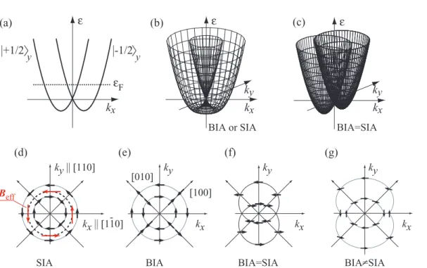
Figure 2 Panel (a) illustrates the SIA/BIA spin splitting due tokxσyterms in the effective Hamiltonian, here| ±1/2ylabel the eigenstates with fixedyspin components. Panels (b) and (c) show schematic 2D band structure withk-linear terms for C2vsymmetry. The energyε is plotted as a function ofkxandkyin (b) with only one type of inversion asymmetry, BIA or SIA, and in (c) for equal strength of the BIA and SIA terms in the Hamiltonian. The bottom panels (d–g) show the distribution of spin orientations at the Fermi energy for different strengths of the BIA and SIA terms. After [28, 58].
by simple symmetry arguments. It follows from the Neu- mann’s principle that the component of a tensor representing a property must remain invariant under a transformation of coordinates governed by a symmetry operation valid for the point group of the crystal [92]. Therefore, the linear in k spin splitting can only occur for those components ofkfor which there are components of the pseudovectorS(the corre- sponding quantum-mechanical operator isσ/2) transforming in the same way. Let us illustrate it for spin aligned along y-direction, i.e., forSy. Figure 1c shows the symmetry ele- ments of asymmetric QWs (point group C2v) together with the transformation ofkxandSyby the mirror reflection inm1
plane. We see, that the reflection in the planem1, as well as in m2, transforms the wavevector componentkxand the pseu- dovector componentSyin the same way:kx →kx,Sy →Sy
for the planem1, see Fig. 1c, andkx → −kx,Sy→ −Syfor the planem2. As the remaining C2-axis also transformskx
andSyequally the linear inkspin splitting connecting these components becomes possible yielding theσykxterms in the effective Hamiltonians (2) and (3). The corresponding band structure is sketched in Fig. 2a. Similar arguments hold for ky andSx (kyσx terms), but not for the out-of-plane com- ponent Sz. Consequently, the linear ink spin splitting for out-of-plane spin is forbidden by symmetry.
The distribution of spin orientation in the states with a givenkcan be visualized by writing the SOI term in the form
HSO =σ·Beff(k), (4)
whereBeff(k) is an effective magnetic field (with absorbed Bohr magneton andg∗-factor [93]), which provides the rel- evant quantization axes. The index “effective” indicates that Beff(k) is not a real magnetic field because it does not break the time-inversion [94]. Consequently, in the presence of SIA/BIA spin splitting the Kramers-relationε↑(k)=ε↓(−k) holds. By comparison of Eq. (4) with Eqs. (2) and (3) one obtains for pure SIA (β=0) and pure BIA (α=0) the effec- tive magnetic fields in forms
BSIAeff =α(ky,−kx), BBIAeff =β(ky, kx). (5)
The effective magnetic field and spin orientations for, both, Rashba and Dresselhaus coupling are schematically shown by arrows in Fig. 2d and e, respectively. Here, it is assumed for concreteness thatα, β >0. For the SIA case, the effective magnetic field and, hence, the electron spin in the eigen- states with the wavevector k are always perpendicular to thek-vector, see Fig. 2d. By contrast, for the BIA contri- bution, the angle between k-vector and spins depends on the direction of k, see Fig. 2e. In the presence of both SIA and BIA spin–orbit couplings (C2v symmetry), the [1¯10] and the [110] axes become strongly nonequivalent.
Fork[1¯10], the eigenvalues of the Hamiltonian are then given byε±=2k2/2m∗±(α−β)k and for k[110] by ε±=2k2/2m∗±(α+β)k. For an arbitrary direction ofk, the energy spectrum of such systems consists of two branches
with the following anisotropic dispersions ε±(k)= 2k2
2m∗ ±k
α2+β2+2αβsin 2ϑk , (6) where ϑk is the angle between k and the x axis [98, 99].
The energy dispersion fork-linear SIA, BIA and combined SIA/BIA terms is illustrated in Fig. 2a–c. In the case of BIA only (α=0) or SIA only (β=0), the band structure is the result of the revolution around the energy axis of two parabolas symmetrically displaced with respect tok= 0. The interplay of SIA and BIA is illustrated in panels (d–g). If the strengths of BIA and SIA are the same, then the 2D band structure consists of two revolution paraboloids with revolu- tion axes symmetrically shifted in opposite directions with respect tok= 0, see Fig. 2c. Now all spins are oriented along
±x-axes as shown in Fig. 2f. In Fig. 2g, we have shown a constant energy surface and direction of spins forα=β.
So far we discussed only k-linear terms in the Hamil- tonian. In fact, in zinc-blende structure based (001)-grown QWs also terms cubic inkare present, which stem from the Dresselhaus term in the host bulk material, Eq. (1). A cubic contribution modifies the Dresselhaus spin-splitting yielding
HBIAcub = γ 2
σxky−σykx
(k2y−k2x). (7)
These terms influence some of spin-dependent phenomena like spin relaxation or WAL and should be taken into account in particularly in narrow band materials and highly doped QWs as well as at high temperature. The correspondingk- cubic effective magnetic field defined via HBIAcub =σ·Bcub
can be conveniently decomposed into Bcub=B(1)cub+B(3)cub, where [96]
B(1)cub= −γk2 4 (ky, kx), B(3)cub= γk3
4 (sin 3ϑk,−cos 3ϑk). (8) As the effective magnetic fieldsBBIAeff andB(1)cubcontaining the first-order Fourier harmonics (∝sinϑkand cosϑk) have the same form [see Eqs. (5) and (8)] they can be combined as
B(1)eff=BBIAeff +B(1)cub=β(k˜ y, kx) (9) with the renormalized Dresselhaus constant
β˜ =β−γk2
4 . (10)
Note that the term γk2/4 scales with k, which for equi- librium electron gas is equal to the Fermi wavevector and respectively, scales with the electron density. In GaAs het- erostructures, cubic inkterms are usually unimportant and in the further consideration we will use ˜βfor analysis of narrow band semiconductors only.
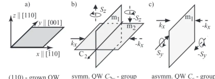
Figure 3 (a) Coordinate system of the (110)-grown III–V QW. (b) Mirror planesm1andm2and C2-axis in symmetric QW belonging to C2vpoint group. (c) Remaining symmetry elements in asymmet- ric QWs (Cspoint group). Arrows in the drawing (b) show that the reflection in the mirror planem1changes the sign of both the polar vector componentkxand the axial vector componentSz, demon- strating that a linear coupling ofkx andSz is allowed under this symmetry operation. This coupling is also allowed by the other symmetry operations (mirror reflection by the planem2 and the C2rotation axis) of the point group yielding theσzkx terms in the effective Hamiltonian. By contrast, the in-plane spinSat reflec- tion in planem2transforms differently compared to any in-plane wavevector components. Arrows in the sketch (c) demonstrate that in asymmetric QWs for whichm2is removed, the coupling between the in-plane spinSyand wavevector componentkxbecomes possi- ble. Same arguments are valid for the coupling ofSxandky. Thus, SIA in asymmetric QWs results in the in-plane effective magnetic field and gives rise to the Dyakonov–Perel spin relaxation for spins oriented along the growth direction.
2.2 Rashba/Dresselhaus terms in (110)-grown zinc-blende structure-based 2DES QWs on (110)- oriented GaAs substrates attracted growing attention due to their extraordinary slow spin dephasing, which can reach several hundreds of nanoseconds [29–33, 35, 36, 38]. As addressed above, the reason for the long spin lifetime in this type of QWs is their symmetry: in (110)-grown QWs, the BIA effective magnetic fieldBeff(k) points into the growth direc- tion [2] therefore spins oriented along this direction do not precess. Hence the Dyakonov–Perel spin relaxation mecha- nism, which is based on the spin precession inBeff(k) and usually limits the spin lifetime of conduction electrons, is suppressed.
Depending on the equivalence or nonequivalence of the QW interfaces, i.e., presence or absence of SIA, the structure symmetry may belong to one of the point groups: C2vor Cs, respectively. While the point group symmetry of symmetric (110)- and asymmetric (001)-oriented III–V QWs is the same (C2v), the Dresselhaus spin splitting links different compo- nents of electron spin and wavevector. The reason for this fact, strange on the first glance, is that by contrast to (001)- oriented QWs for which mirror reflection planesm1andm2
are oriented normal to the QW plane, see Fig. 1, in symmetric (110) QWs one of the planes, saym2, coincides with the plane of QW. The symmetry elements of symmetrical (110)-grown QWs are shown in Fig. 3b. By simple symmetry analysis we find that the only wavevector and spin components trans- forming in the same way are kx andSz, i.e., the effective magnetic field caused by the spin splitting points along the
Figure 4 (a–c) Crystallographic directions and effective magnetic fields for the lower conduction subband in (110)-grown QW. Plots (a–c) sketchBeff(k) for BIA, SIA, and SIA/BIA interplay, respectively. Note that forα=0, panel (a),Beff(k) is aligned alongzaxis for anykapart fromkyat which states are spin degenerated. (d) Calculated values of the spin splitting for states lying on a circle in the kx–kyplane withk=0.01 ˚A−1for variousα/βratio. Here,βis 10−9eV cm is assumed for calculations. (e) Spin lifetimes as a function of the ratio of the SIA and the BIA parameters. The labelsτx,y,zrefer to the spin relaxation tensor in the axesx,y, andz. The latter two lie in (y, z) plane and are tilted to the axesyandz, see Table 1, by the angleθ=arctan (α/β). Data are given after [103].
growth axis. The reflection of these components in the m1 mirror plane resulting inkx→ −kx,Sz→ −Sz, are shown in Fig. 3b. The corresponding Hamiltonian has the form
HBIA =βσzkx. (11)
SIA removes the mirror reflection planem2and enables spin splitting for the in-plane spin components. This is illus- trated in Fig. 3c showing that in asymmetric (110)-grown structureskx andSy transform equally. Additional terms in the Hamiltonian caused by the symmetry reduction have the same form as the Rashba terms in (001)-oriented QWs Eq. (3). The in-plane effective magnetic field due to Rashba spin–orbit coupling results in spin dephasing even for spins oriented along growth direction and the benefit of (110) QWs disappears [100]. The energy spectrum of such sys- tems consists of two branches with the following anisotropic dispersions
ε±(k)=2k2 2m∗ ±k
α2+β2cos2ϑk. (12) Like in (001) QWs, the different forms of the BIA and SIA terms result in their interference substantially affecting the band spin-splitting. The spin splitting and calculated spin relaxation times for someα/β-ratios are shown in Fig. 4d and e, respectively. Moreover, thek-cubic terms for symmetric (110) QWs result in the effective magnetic field also pointing in the growth direction, so they do not lead to spin relaxation of the normal spin component as well.
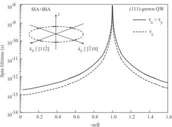
2.3 Rashba/Dresselhaus terms in (111)-grown zinc-blende structure-based 2DES QWs grown along [111]-direction draw attention primary due to the possible suppression of the Dyakonov–Perel spin relaxation mech- anism for all spin components [37, 39–42, 103–105]. The reason for this interesting feature is the formal identity of thek-linear Dresselhaus and Rashba Hamiltonians, which both have a form of Eq. (3) but imply different constants,β andα, respectively [2, 103]. As a result, the total spin–orbit Hamiltonian can be written in form
HSO=(β+α)(σxky−σykx). (13) The corresponding effective magnetic fields are shown in the inset in Fig. 5. A straightforward consequence of Eq. (13) is that conduction band becomes spin degenerate to first order inkforanywavevector direction in the case that BIA and SIA coefficients would have equal magnitude but opposite signs, i.e.,β= −α. The most significant feature of this configura- tion is that the spin lifetimes would become tremendously increased. The dependence of the in-plane and out-of-plane spin relaxation times on the ratio between the Rashba and Dresselhaus coefficients is shown in Fig. 5.
2.4 Rashba/Dresselhaus terms in (113)-, (112)-, (013)-, and miscut (001)-grown zinc-blende structure-based 2DES So far we discussed widely spread configurations of zinc-blende structure-based QWs.
To be complete, we also address the band spin splitting in QWs grown in more exotic directions. These are (113)-,
Figure 5 Spin lifetimes in (111)-grown QW as a function of the SIA/BIA-ratio. Inset sketchesBeff(k) for QWs with any values of SIA/BIA ratio. Note that in the case ofβ= −αeffective magnetic fieldBeff(k)=0 for any electron wavevector and states become spin degenerated. Data are given after [103].
(112)-, and (013)-oriented 2DES as well as (001) miscut structures. The former orientation is usually used for growth of high mobility p-type GaAs QWs, which attracted notable attention due to the possibility to obtain long spin relaxation times [106–112]. QWs of (112)- and (013)-orientations are mainly used for growth of HgTe 2DES, which become particularly important since discovery of the topological insulator states in this material [113, 114] opening the possibility to study physics of Dirac fermions in the systems with the strong SOI. Miscut heterostructures are usually MOCVD-grown on slightly tilted (001) substrates.
Zinc-blende structure based (113)-, (112)- andmiscut (001)-oriented 2DES belong to the symmetry point group Cs, which contains only two elements, the identity and one mirror reflection plane,m, being normal to the 2DES plane.
A natural coordinate system for these structures grown in z-direction arex- normal to the planemandy-orthogonal to x and z, cf. Table 1 for (113)-grown QWs. Then BIA spin-splitting is given by
HBIACs =β1σxky+β2σykx+β3σzkx , (14) while the SIA Hamiltonian is again described by a universal form of Eq. (3). A particular feature of such 2DES com- pared to (001)-grown QWs is the appearance of the spin splitting for spins oriented along the growth direction. Note that the spin–orbit coupling terms in asymmetric (110) QWs, which have Cs symmetry, are also described by the sum of the Hamiltonians Eqs. (3) and (14).
QWs prepared on (013)-oriented substrates belong to the trivial point group C1lacking any symmetry operation except the identity. This is true even for structure-symmetric QWs, where SIA is absent. Hence, symmetry does not impose any restriction on the relation between the spin and wavevector
components:
HSOC1=
lm
Λlmσlkm. (15)
Herel=x, y, zandm=x, y. Since all components of the pseudotensorΛmay be different from zero the spin splitting is allowed for any relative directions of spin and electron wavevector. Moreover, the ratio between the components of the tensorΛcan be changed in nontrivial way (including the sign inversion) by varying the experimental conditions like, e.g., sample temperature or carrier density.
To complete the picture of spin splitting in zinc-blende structure-based QWs, we note that symmetry reduction can also be obtained by, e.g., applying stress, fabricating ungated/gated lateral superlattices, and growing quasi one- dimensional wires. The form of the spin–orbit Hamiltonian in such structures depends on the resulting symmetry (C2v, Cs, or C1) and is described by the corresponding equations discussed above.
2.5 Wurtzite-type semiconductor structures Wurtzite-type bulk semiconductors, like GaN or InN, are described by a nonsymmorphic space group C46vcontaining a nontrivial translation. However, the physical effects are determined by the point-group symmetry. The point group of wurtzite semiconductors C6v is gyrotropic [84] and, therefore, allows the linear in wavevector spin splitting. As it was pointed out in Ref. [3] in these media the spin–orbit part of the Hamiltonian has the form
Hbulk=β(σ×k)z, (16)
where the constantβ is solely due to BIA. Here,z-axis is directed along the hexagonal c-axis [115]. In heterostruc- tures, an additional source ofk-linear spin splitting, induced by SIA becomes possible. If both, bulk and structure asym- metries, are present the resulting coupling constant is equal to the sum of BIA and SIA contributions to the spin–orbit part of the Hamiltonian. Thus, for 2DES based, e.g., on GaN or InN grown in [0001] direction, the total spin–orbit part of the Hamiltonian has exactly the same form as that for (111)-grown zinc-blende based structures discussed in Section 2.3:
HSO =(β+α)(σxky−σykx), (17) and forβ= −αconduction bands become spin degenerate to first order inkforanywavevector direction.
2.6 SiGe QWs Finally, we briefly discuss SiGe QWs.
Since both Si and Ge possess inversion center SiGe het- erostructures do not have BIA. However, both IIA, with a BIA-like form of the Hamiltonian [117], and SIA may lead to k-linear terms [116, 118–122]. The symmetry of Si/(Si1−xGex)n/Si QW in the absence of SIA depends on the numbernof the mono-atomic layers in the well. In the case of
metry of QWs isD2hwhich is inversion symmetric and does not yieldk-linear terms. An odd number ofn, however, inter- changes the [1¯10] and [110] axes of the adjacent barriers and reduces the symmetry to D2d[116, 119] with the same impli- cation treated above for zinc-blende structure-based QWs, see Eq. (2) for IIA. The symmetry reduction of SiGe struc- tures to C2vmay be caused by, e.g., an electric field (external or built-in) applied along the growth direction. If the structure is grown along the low-symmetry axisz[hhl] with [hhl]= [001] or [111], the point group becomes Cs(see, e.g., [116]) and contains only two elements, the identity and one mirror reflection plane (1¯10). Here, the spin splitting is described by equations presented in Section 2.4.
3 Determination of SIA and BIA spin splittings by photogalvanic measurements A direct way to explore the BIA and SIA interplay, which does not require knowledge of microscopic details, is based on the phe- nomenological equivalence of Rashba/Dresselhaus linear in kspin splitting given by
HSO =
lm
Λlmσlkm, (18)
whereΛlm is a second rank pseudo-tensor, with other phe- nomena also described by a linear coupling of a polar vector, like current, and an axial vector, like electron spin.
Indeed, all these effects are described by second rank pseudo- tensors whose irreducible components differ by a scalar factor only and, consequently, are characterized by the same anisotropy. In semiconductor 2DES, there are three effects, which belong to a large class of photogalvanic phe- nomena [80, 82, 83, 123, 124] and like Rashba/Dresselhaus linear in k spin splitting are described by such a kind of the second rank pseudo-tensors. These phenomena are the spin-galvanic effect (SGE) [125, 126], the circular photo- galvanic effect (CPGE) [127, 128], and magneto-gyrotropic effect (MPGE) [60, 129]. They link the dc electric cur- rent with nonequilibrium spin (SGE), angular momentum of photons (CPGE) or an external magnetic field (MPGE).
In analogy to the band spin-splitting and based on the equivalence of the invariant irreducible components of the corresponding pseudo-tensors, these currents can be decom- posed into Rashba and Dresselhaus contributions, which can be measured separately. Taking the ratio between these contributions cancels the scalar factor, which contains all microscopic details [33, 58–60, 64, 130, 131]. As the phys- ical mechanisms of the effects under consideration are discussed in a great details in several reviews and mono- graphs [11, 28, 80, 83, 145] and are in fact inessential for the study of the the spin-splitting anisotropy we focus below on their symmetry analysis. We start with the general equations for each effect and briefly address their origin.
(i) Spin-galvanic effect. The spin-galvanic effect consists in the generation of an electric currentjdue to a nonequilib- rium spinSand is caused by an asymmetric spin relaxation
spin-galvanic effect generally does not need an optical exci- tation but may also occur due to optical spin orientation yielding a spin photocurrent. The resulting electric current is given by
jl =
m
QlmSm. (19)
(ii) Circular photogalvanic effect. The CPGE is another phenomenon, which links the current to the spin-splitting in heterostructures [28, 80]. It steams from the selective pho- toexcitation of carriers ink-space due to optical selection rules for absorption of circularly polarized light and is given by
jl =
m
χlmeˆmPcirc|E|2 , (20) where ˆeis the unit vector pointing in the direction of light propagation, andE is the complex amplitude of the elec- tric field of the electromagnetic wave. The direction of the resulting electric current reverses at inversion of the radiation helicityPcircbeing a fingerprint of CPGE.
(iii) Magneto-gyrotropic effect. MPGE is the electric cur- rent excitation by normally incident radiation in the presence of an external magnetic fieldB[143, 144]. It may be caused by the spin or orbital mechanisms. The spin-driven MPGEs are based on spin–orbit coupling in 2DES with SIA and BIA.
The electric current is generated due to a spin-dependent energy relaxation of electrons heated by radiation in the Zee- man split subbands. The orbital mechanism is caused by a magnetic-field-induced scattering asymmetry [195]. For unpolarized radiation MPGE is given by
jl =
m
ξlmBm|E|2 . (21)
Equation (18) and (19)–(21) have in common that all these phenomena link linearly vector and pseudovector components. Therefore, as addressed above, they are char- acterized by the same anisotropy in space, according to the Neumann principle [92], the equivalence of the components of the pseudo-tensorsΛ,Q,χ, andξcan be used to evaluate the ratio between SIA and BIA strength as well as to deter- mine their relative sign [33, 58–60, 64, 130, 131]. Note that the same arguments are valid for the inversed SGE [132].
This can be illustrated on example of the spin-galvanic effect where an electric current is caused by asymmetric spin relaxation of nonequilibrium spin polarized carriers in the system with a spin–orbit splitting of the energy spectrum, for reviews see [28, 81, 83]. While in general the spin-galvanic effect does not need optical excitation the SIA/BIA interplay can most convenient be studied applying circularly polarized radiation for spin orientation of carriers resulting inS.
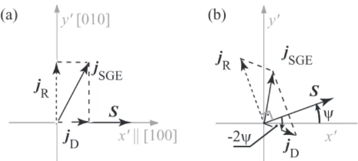
The SGE currentjSGE is linked to the average spin by a second rank pseudo-tensor Q, see Eq. (19), and can be
Figure 6 Spin-galvanic current and its SIA and BIA components in a (001)-grown QW: (a) for the in-plane average spin direction aligned alongx, (b) forSgiven by arbitrary angleΨ. After [58, 59].
presented via the parameters of spin–orbit splitting in (001) QWs as follows
jSGEx =Q(β˜ −α)Sy, jySGE=Q(β˜ +α)Sx, (22) where Qxy=Q(β˜ −α), Qyx=Q(β˜ +α) with ˜Q being a constant determined by the kinetics of the SGE, namely by the characteristics of momentum and spin relaxation pro- cesses. In the coordinate system with cubic axes (x[100], y[010]) Eq. (19) can be conveniently presented in the form
jSGE=Q˜
β −α α −β
S , (23)
demonstrating that for spin aligned alongx orymeasure- ments of the SGE current parallel and perpendicular to S directly yield theα/β-ratio. This is sketched in Fig. 6a show- ing the average spinSxand the spin-galvanic currentjSGE, which is decomposed intojx =jDandjy =jRproportional to the Dresselhaus constantβ and the Rashba constantα, respectively. This configuration represents the most conve- nient experimental geometry in which the ratio of the currents measured alongx- andy-axes yields
α
β =jy(Sx)
jx(Sx) . (24)
We emphasize that this geometry unambiguously shows whether the Rashba or Dresselhaus contribution is dominat- ing. Furthermore, these measurements provide experimental determination of both the ratio and the relative sign of the Rashba and Dresselhaus constants.
Analogously to the spin splitting, symmetry arguments yield that for arbitrary orientation of the average spinSthe currentjRis always perpendicular toSwhile the currentjD encloses an angle−2ΨwithS, whereΨis the angle between Sand thex-axis. The strength of the total currentjSGEis given by the expression
jSGE=
j2R+jD2 −2jRjDsin 2Ψ , (25)
which has the same algebraic form as the spin–orbit term in the band structure, see Eq. (6). Taking the ratio between Rashba and Dresselhaus current contributions can- cels the scalar factor ˜Q, which contains all microscopic details [58, 59]. Hence, by mapping the magnitude of the photocurrent in the plane of the QW theα/β-ratio can be directly extracted from experiments. Similar consideration can be made for the circular photogalvanic and MPGEs.
The details of the method can be found in Refs. [33, 58–
60, 80, 131, 143, 144].
An important advantage of the discussed method is that it applies to the photogalvanic effects, which are very general and have been detected in a large variety of low-dimensional semiconductor structures of a very different designs, for recent reviews on these effects see [80, 83, 91, 144, 145], including topological insulators and other systems with Dirac fermions [146–156]. The studies of the last decade show that these effects in 2DES can be detected in a wide tem- perature range including technologically important room temperature and applying radiation in a wide frequency range, from microwaves up to visible light. It is important to note that all photogalvanic effects addressed above are caused by the terms B(1)eff(k) andBSIAeff(k) in the effective magnetic field, which are first angular harmonics of ϑk, see sec- tion 2.1. The rest cubic terms in the effective magnetic field B(3)eff(k)∝sin 3ϑk,cos 3ϑkdo not result in the discussed pho- togalvanic currents, however, they modify the spin-splitting and may affect spin relaxation and the anisotropy of spin-flip Raman scattering [48, 51, 79, 82, 157–159]. Consequently, photogalvanics based methods provide the information on the SIA/BIA terms given by Rashba constantαand renormalized Dresselhaus constant ˜β.
4 Experimental technique Photogalvanics have been used to probe SIA/BIA interplay in a large variety of low-dimensional structures of different design yielding information on the modification of the SIA/BIA-ratio upon changing of various macroscopic parameters like crystallo- graphic orientation, doping position, quantum well widths, temperature, etc. Zinc-blende and wurtzite semiconductor- based heterostructures as well as SiGe QWs were studied.
For optical excitation, a great variety of radiation sources have been used including pulsed and cw molecular THz lasers [81, 146, 160–163], free electron lasers [81, 169, 164–
168], CO2lasers [116, 168, 170], Ti-sapphire and other solid state lasers [62, 65, 171], semiconductor lasers [172, 173], He–Cd laser [174], time-domain THz systems [61, 81, 175–
177], conventional Gunn diodes [178] etc. While SIA/BIA interplay has been studied in a wide frequency range from microwaves to the near infrared, microwaves/terahertz radi- ation are particularly suitable for the methods addressed in the previous section. First of all, in the microwave/terahertz range photogalvanics may be observed and investigated much more easily than in the visible or near infrared ranges, where strong spurious photocurrents, caused by other mech- anisms like the Dember effect [81], photovoltaic effects at contacts, etc., mask the relatively weak spin photogalvanic
optical spin orientation using interband transitions, terahertz radiation excites only one type of charge carrier yielding monopolar spin orientation, giving the information about spin splitting in one subband. Furthermore, electrons excited by terahertz radiation remain close to the Fermi energy, which corresponds to the conditions of electric spin injection.
Obviously photocurrent measurements applying radia- tion with photon energies smaller than the band gap require free carriers. Therefore, photogalvanic methods are applied to study either doped low-dimensional systems or undoped structures additionally exposed to light resulting in the photogeneration of electron–hole pairs. In the latter case, photogalvanics is caused by the superposition of electron and hole contributions, which complicates the analysis of the spin splitting in a particular band. Experimental geometry depends on the type of phenomenon used for the SIA/BIA mapping (CPGE, SGE, or MPGE) and crystallographic orientation of the studied low-dimensional structure.
CPGE- and SGE-based methods require circularly polarized radiation at oblique, or, for low symmetric structures, normal incidence. For MPGE- [60, 179] and, in some cases, SGE-based methods [58], a small external magnetic field is needed. Details of the experimental configurations can be found in Refs. [33, 58–60, 80, 131, 143].
In the most frequently used geometry, rectangular shaped 3×5 mm2 size samples with an edge oriented parallel to one of the reflection planes have been studied. The latter can in most cases be naturally obtained by cleaving the sam- ple. Several pairs of contacts, being needed for electrical measurements, are made in the middle of the edges and corners of the squared sample. Although this geometry of contacts is sufficient for study of SIA/BIA anisotropy, the results accuracy can be increased by using a larger number of contact pads forming a circle [58, 131]. The photocurrent J(θ), whereθ is the polar angle, is measured in unbiased structures via the voltage drop across a 50Ω load resistor with a fast storage oscilloscope or applying standard lock- in technique [28]. We note that a pure optical method to measure photogalvanic currents, which provides a unique access to characterization of SIA/BIA in a contactless way, has been developed [61, 175, 180, 181]. It is based on the terahertz emission resulting from the photogalvanic currents generated by picosecond pulses of near infrared radiation.
The physical principle is just the same as of the Auston switch [182, 183] used for generation of THz radiation in the terahertz time-domain spectroscopy [81, 176, 177].
5 Interplay of BIA and SIA in (001)-, (110)-, and (111)-grown III–V 2D systems
5.1 Tuning of structure inversion asymmetry by the ␦-doping position In this section, we discuss the influence of the δ-doping position, quantum well width and growth conditions on SIA and BIA in III–V semi- conductors based (001)-oriented quantum well structures.
We begin with MPGE investigations of Si-δ-doped n-type GaAs/Al0.3Ga0.7As structures grown by molecular-beam epi-
Figure 7 (a) The ratio of the SIA and BIA contributions to the MPGE,Jx/Jy, as a function ofχ. The triangles show the result for sample grown atTδ=490◦C, the circles demonstrate the data for all other samples grown atTδ ≈630◦C. Insets show the QW profile and the doping positions forl < rand forl > r. (b) Depen- dence ofJ/Pns on the parameterχ, herensis the carrier density, andP is the radiation power. The photocurrents Jy and Jx are measured along and normal toBy. Full and open symbols show JxandJy, respectively (triangles are the data for sample fabricated with reduced temperature during theδ-doping (Tδ=490◦C)). Inset shows experimental geometry. After [60].
taxy at typical temperatures in excess of 600◦C. The insets in Fig. 7 sketch the conduction band edges of different QW structures together with the correspondingδ-doping position.
All QWs have the same width of 15 nm but differ essentially in their doping profile. The degree of the doping asymmetry can be conveniently described by the parameter
χ= l−r l+r,
where l and r are the spacer layer thicknesses between QW and δ-layers. Variation of individual BIA and SIA contributions as well as their ratio have been studied apply- ing magneto-gyrotropic photogalvanic effect [60]. In these experiments, unpolarized terahertz radiation at normal inci- dence was used for excitation of QW structure subjected to
an in-plane magnetic field applied along a cubic axisy. BIA and SIA photocurrent contributions have been obtained by measuring the current along and perpendicular to the mag- netic field, i.e.,JyandJx, respectively. The ratio of SIA/BIA contribution as a function of the parameterχ is shown in Fig. 7a demonstrating that it has a strong dependence on the doping position and, moreover, changes its sign forχ≈0.1.
The analysis of the individual contributions shown in Fig. 7b indicates that in all structures BIA remains almost unchanged and the SIA is solely responsible for the variation of the band spin splitting with the parameterχ.
The variation of the parameterχshows that SIA is very sensitive to the impurity potential and its magnitude and the sign can be controlled by the δ-doping position. The fact that in nominally symmetric QWs withχ=0 SIA yields a substantial photocurrent signal reflects the dopant migration along the growth direction (segregation) during molecular beam epitaxial growth. This conclusion is supported by the MPGE measurements in symmetrically doped sample (χ= 0) fabricated with reduced temperature during theδ-doping (Tδ=490◦C). At this conditions segregation is suppressed and SIA vanishes, see Fig. 7.
Investigation of the structures with different band profile and δ-doping positions show that the largest value of the SIA/BIA ratio is obtained in a single heterojunction [59].
While optical experiments on spin relaxation in undoped samples demonstrate that the variation of the band profile does not substantially affect SIA [70, 71] in doped structures it seems to play an important role. Indeed in structures with strongly asymmetric potential profile like triangular confinement potential or stepped QWs, the electron function is shifted to one of the interfaces and is strongly affected by the impurity Coulomb potential [184]. The second reason for the enlarged SIA/BIA ratio in wide 2D structures is the decrease of the Dresselhaus SOI, which is given by the size quantization of the electron wave vectorkzalong the growth direction z. Theory shows that BIA for a QW of width Lw should change after
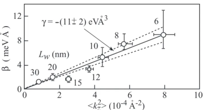
k2z ∝1/L2w [2]. This behavior was experimentally confirmed by optical monitoring of the angular dependence of the electron spin precession on the direction of electron motion with respect to the crys- tallographic axes [188, 189]. The latter has been obtained driving a current through the structure. A set of (001)-grown GaAs/AlGaAs QWs with different well widths between 6 and 30 nm and fixed parameterχhave been studied demon- strating a linear increase of the Dresselhaus splitting with the increase of the confinement parameter
k2z . The linear fit presented in Fig. 8 yields the bulk Dresselhaus coefficient, cf. Eq. (1), for GaAs,γ=(−11±2) eV ˚A3. The data also allowed to measure the cubic inkDreeselhaus term showing that in GaAs it is substantially smaller than the linear one (from 2 up to 30 times, for 3 and 6 nm QWs, respectively).
The experiments on the optical monitoring of the spin precession as a function of Lw also provided information on the sign of the g∗-factor confirming its sign change at Lw =7 nm [188]. This inversion is mostly caused by the opposite signs of theg∗-factor in the GaAs with respect to the
Figure 8 Measured linear inkBIA spin splitting,β, versus kz2 . Circles and square are the data of Refs. [188] and [189], respectively.
Solid line is the fit to−γ
kz2 and dotted lines are 95% confidence interval. Error bars show the estimated uncertainty in the fitted slope.
Horizontal bars depict±0.5 nm variation inLw and vertical bars indicate 30% variation in carrier density. After [188].
AlGaAs barrier and the fact that for narrow QWs the electron wave function deeply penetrates into the barrier [190–194].
The change of sign is of particular importance for the stud- ies of the magneto-photogalvanic effects resulting from the spin-related roots. As discussed above, the MPGE photocur- rent is proportional to the Zeeman band spin splitting and is determined by the effective Land´e factorg∗. The same set of samples as that investigated in the work of Walser et al. [188]
was previously used to provide an experimental evidence for spin-related roots of the current formation in most of (001) GaAs QWs at room temperature [195]. Figure 9 shows the MPGE photocurrent JL as a function of Lw. For compar- ison, g∗ extracted from the time-resolved Kerr rotation is also plotted. As an important result, Fig. 9 demonstrates that the photocurrent, similarly to theg∗-factor, changes its sign upon the variation ofLw. However, there is a difference in the zero points: While the g∗=0 at Lw =7 nm, the cur- rent vanishes forLw≈10 nm. A small current detected atg∗ inversion point, at which spin mechanism of MPGE is dis- abled, is caused by the orbital mechanism [195, 196], which is almost independent onLw. For other QW widths, the spin related mechanism dominates the total current. The dominat- ing contribution of spin mechanisms in GaAs QWs is also demonstrated for the circular MPGE [195], where in-plane spin density required for spin-galvanic effect is created via optical excitation and the Hanle effect [59, 126].
Circular photogalvanic and spin galvanic effects have also been applied for studying the SIA/BIA-ratio in (001)- oriented doped InAs/InGaSb QWs and InGaAs/InAlAs QW structures [58, 59]. In InAs/InGaSb QWs, the measurements yield the value in the range 1.6–2.3, which agrees well with theoretical results [197] predicting a dominating Rashba spin–orbit coupling for InAs QWs and is also consistent with experiments applying other transport methods [50, 198].
Note that the Rashba term is very sensitive to details of the sample growth and further treatment. Furthermore, photogal- vanic methods have been applied to study the SIA/BIA-ratio in a set of InGaAs/InAlAs QW structures with semitrans-
Figure 9 Dependence of the MPGE (circles) on Lw obtained at room temperature, By= ±1 T and photon energy ω= 4.4 meV and corresponding g∗-factors (triangles determined by by TRKR [195] and squares by comparison of BIA and Zeeman spin splitting [188]). The inset shows the experimental geometry.
After [195].
parent gate [131]. The measurements supported by the WAL experiments permitted to find a proper QW design for the realization of the persistent helix conditions. These results are discussed in Section 5.2.
To complete the picture, we note that BIA and SIA induced CPGE, SGE, and MPGE have been also observed in (001)-oriented InSb/(Al,In)Sb and HgTe/CdHgTe quantum well structures [65, 199–202]. These narrow band materials are of particular interest for spin physics because they are characterized by high mobility and small effective masses as well as by a very large g∗-factor and spin–orbit split- ting [203–207]. So far, while confirmed the band spin splitting, most of the studies have been aimed to the mecha- nisms of the current formation in these novel materials, which can now be extended by special studies aimed to SIA/BIA interplay.
The experiments described above were carried out apply- ing terahertz/microwave radiation. The dominant mechanism of the spin–orbit splitting, however, can also be determined from study of photogalvanics caused by interband absorp- tion [208–210]. An interesting possibility to study the spin splitting provides the study of the CPGE spectra [130, 208]:
the SIA-induced CPGE photocurrent has a spectral sign inversion in contrast to the BIA-one. The interplay of the Rashba/Dresselhaus has been investigated in applying CPGE in Ref. [66, 211–213] and MPGE in [173].
To conclude this part, the observation of the sign reversal of the Rashba/Dresselhaus-ratio upon changing theδ-doping position in the heterostructure together with quantum well width dependence of BIA can be used for growth of 2D struc- tures with controllable spin splitting. It is important to note that measurements have also been carried out at technolog- ically important room temperature at which other methods based on spin-relaxation or antilocalization experiments can not be applied. Thus, the measurements of photogalvan- ics can be used as a necessary feedback for technologists
constant or for structures with equal Rashba and Dressel- haus spin-splittings. The latter will be discussed in the next section.
5.2 Quantum well design requirements for long spin relaxation times in (001)-grown QWs and realization of persistent spin helix The strongest anisotropy of the spin–orbit splitting can be achieved in zinc-blende semiconductor-based (001)-grown QWs with thek-linear Rashba and Dresselhaus terms of equal strength, α=β. Under these circumstances and for unessential con- tribution ofk-cubic BIA terms, the spin splitting vanishes in certaink-space direction. Moreover, the resulting effec- tive magnetic fieldBeff(k) is aligned along one of the110 crystallographic axes for any wavevectork, see Fig. 2g. Con- sequently, it becomes ineffective for spins oriented along this axis. In this particular case, the interference of the Dres- selhaus and Rashba terms leads to the (i) disappearance of an anti-localization [49, 50]) suppression of the Dyakonov–
Perel relaxation for spin oriented along Beff [21–23], (ii) lack of SdH beating [214, 215], and (iii) makes possible the formation of the PSH. The latter represents a new state of such a spin–orbit coupled system, which was predicted in Ref. [25] and experimentally observed in GaAs 2DES with weakk-cubic Dresselhaus terms (see, e.g., [216]) applying transient spin-gating spectroscopy [26, 27]. In this particular case, spin precession around the fixed axisBeff[1¯10] sup- ports the space oscillations of the spin distribution in the [110]
direction with a periodπ2/(2m∗α). Indeed, the precession angle for electron spins aligned in the (1¯10) plane equals to 2πafter passing each period, while the spins oriented along [1¯10] direction are intact at all. This demonstrates the stability of the space oscillating state (PSH state) to the spin preces- sion. The specific spin splitting forα=βserving novel ways for spin manipulation attracted valuable attention. There has been much effort in this field both theoretically with new device proposals [24, 46] and discussion of the PSH forma- tion [217–222] as well as experimentally with the aim to obtain SIA equal to BIA [26, 27, 55–58, 60, 131].
The design and growth of structures with a defined SIA/BIA-ratio needs techniques for its control. Generally, the requirement ofα=β can be fulfilled by the variation of both Rashba and Dresselhaus terms, which depend on a number of macroscopic parameters, such as material of quan- tum well, quantum well width, doping profile and growth temperature, gate voltage, carrier density, sample temper- ature, etc. The Dresselhaus SOI is primary determined by the material properties and quantum well width and is fixed for a given quantum well [223]. Therefore, the only way to realizeα=βin a given QW is to control the Rashba term.
The latter can be achieved by the position of the asymmetric δ-doping [26, 60, 131], see Section 5.1, or by the applica- tion of a gate voltage [131, 198, 224–226]. Figure 7a shows that in 15 nm wide GaAs QWs the α= ±β condition is achieved forχ=0 and χ≈0.17. In these structures, the ratio of the BIA and SIA related photocurrents|Jx/Jy| is
![Figure 9 Dependence of the MPGE (circles) on L w obtained at room temperature, B y = ± 1 T and photon energy ω = 4.4 meV and corresponding g ∗ -factors (triangles determined by by TRKR [195] and squares by comparison of BIA and Zeeman spin splitting [188]](https://thumb-eu.123doks.com/thumbv2/1library_info/5613620.1691729/12.892.78.426.143.362/dependence-obtained-temperature-corresponding-triangles-determined-comparison-splitting.webp)