resolved spin transport phenomena in GaAs based
structures
Dissertation
zur Erlangung des Doktorgrades der Naturwissenschaften (Dr. rer. nat.)
der Fakult¨at f¨ur Physik der Universit¨at Regensburg
vorgelegt von
Roland V¨olkl
aus Weiden i.d.OPf.
Oktober 2013
Pr¨ufungsausschuß: Vorsitzender: Prof. Dr. Jaroslav Fabian 1. Gutachter: Prof. Dr. Christian Sch¨uller 2. Gutachter: Prof. Dr. Sergey D. Ganichev Weiterer Pr¨ufer: Prof. Dr. Dieter Weiss
Contents i
1 Introduction 1
2 Basics 5
2.1 Material properties . . . 5
2.1.1 GaAs / AlGaAs structures . . . 5
2.1.2 Ferromagnetism in Gallium manganese arsenide . . . 11
2.2 Spin in Semiconductors . . . 13
2.2.1 Generation of a spin polarization . . . 14
2.2.2 Spin-orbit interaction and symmetry . . . 21
2.2.3 Spin dynamics . . . 26
2.2.4 Spin dephasing mechanisms . . . 27
2.2.5 Spin in GaAs bulk . . . 32
2.2.6 Spin in (110)-grown GaAs quantum wells . . . 33
2.3 Spin transport phenomena . . . 36
2.3.1 Scattering time and mobility . . . 36
2.3.2 Drift and diffusion . . . 38
2.4 Dynamic nuclear polarization (DNP) . . . 42
3 Experimental methods 45 3.1 Magneto-optic Kerr/ Faraday effect . . . 45
3.2 Hanle-MOKE technique . . . 48
3.2.1 Hanle-MOKE and electrical spin injection . . . 51
3.3 Photoluminescence spectroscopy . . . 53
3.4 Gating . . . 55
3.5 Experimental setup . . . 56
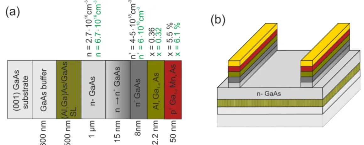
4 Electrical Spin-injection into GaAs bulk from (Ga,Mn)As contacts 61 4.1 The sample structure . . . 61
4.2 Characterization of the sample . . . 64
4.3 Spin dynamics . . . 67
4.3.1 Spin lifetimes . . . 68
4.3.2 Bias dependence . . . 70
4.4 Spin drift and diffusion . . . 72
4.4.1 Spin diffusion . . . 72
4.4.2 Spin drift . . . 74
4.5 Dynamical nuclear polarization detected via combined electrical and op- tical injection . . . 76
i
5 Spin dynamics and spin transport phenomena in high-mobility (110)-
grown quantum wells 81
5.1 The sample structure of the high-mobility (110)-grown quantum wells . 81
5.2 Spin dynamics in high-mobility (110)-grown quantum wells . . . 85
5.2.1 Carrier dynamics of the (110)-grown quantum well samples . . . 85
5.2.2 Spin dephasing in (110)-grown quantum wells . . . 88
5.2.3 Spin polarization in (110)-grown quantum wells . . . 103
5.3 Spin diffusion in (110)-grown quantum wells . . . 109
5.3.1 Gate-controlled spin diffusion . . . 117
5.4 Electric field dependent spin transport in (110)-grown quantum wells . . 119
5.5 Dynamic nuclear polarization in (110)-grown quantum wells . . . 123
6 Summary 127
Bibliography 131
Symbols and abbreviations 159
Introduction
Despite W. Paulis statement that “One should not work on semiconductors. They are a mess. Who knows whether semiconductors exist at all.” 1 semiconductor technologies have become the foundation of modern information technology. At Bell Laboratories, the first step in developing this technology that is indispensable today was done, by implementing a transistor based on Germanium [Bar48] 2. W. Shockleys proposal of a field effect transistor [Sho52] and J. S. Kilbys invention of the integrated circuit [Kil63;
Kil76] then laid the foundation of today’s electronics. Advances in the fabrication of semiconductor structures for instance Metal-Organic-Vapor-Phase Epitaxy (MOVPE) [Man68] and Molecular-Beam Epitaxy (MBE) [Art68; Cho71], allowed the development of low-dimensional structures such as quantum wells (2D), quantum wires (1D), and quantum dots (0D). Quantization effects become apparent when the movement of car- riers is restricted in one or more degrees of freedom on a scale comparable to their de Broglie wavelength λdB =h/p. Quantum mechanical effects, such as the quantum Hall effect [Kli80] or the Aharonov-Bohm-effect (electron interference) [Aha59; Web85]
could be observed in those structures. Furthermore, the possibility to fabricate het- erojunctions resulted in structures with high carrier mobilities, utilized for example in high-electron-mobility transistors (HEMT) [Mim80], and the proposal of semiconduc- tor lasers [Kro63; Kro01; Hal62] 3. Since the first works of Kilby computing hardware has developed enormously. The well-known Moore’s law reflects this evolution, and it states that the amount of transistors on an integrated circuit doubles approximately every 18 months [Moo65]. Eventually, this minimization creates problems when the size approaches an atomic scale and quantum mechanical effects gain impact. Moreover, parasitic capacitances, and leakage currents create problems in the low-scale planar electronics [Tho06]. The development of new technologies is therefore inevitable.
To improve the efficiency of electronic devices and to enrich them with new func- tionalities is the goal of spintronics, where the intrinsic spin replaces the charge in the elements of modern information manipulation (logic, storage, and communication).
Metal-based spintronics already enjoyed great success in the proposal of the giant mag- neto resistance (GMR) [Bai88; Bin89] 4, which became a basis in developing modern storage devices. Modern hard disk read heads, as well as non-volatile memory, such as the magnetoresistive random access memory (MRAM), are developed on this basis.
1From a letter of Wolfgang Pauli to Rudolph Peierls, 1931.
2Awarded with the Nobel Prize in Physics 1956 to W. B. Shockley, J. Bardeen, W. H. Brattain.
3The Nobel Prize in Physics 2000 was awarded to Z. I. Alferov, H Kroemer and J. S. Kilby for basic work on information and communication technology.
4A. Fert and P. Gr¨unberg received the Nobel Prize in Physics in 2007 for the GMR concept.
1
After Johnson and Silsbee’s observation of the injection of spin-polarized electrons from a ferromagnet into a metal [Joh85; Joh88], the proposal of a spin field effect tran- sistor (sFET) drew a lot of attention and boosted the research efforts in semiconductor spintronics. In this concept, as well as in the experiments presented here, the spin- orbit interaction (SOI), which is strong in semiconductors compared to a free electron, plays a central role. The influence of SOI is essential in various transport experiments.
Prominent examples are weak (anti) localization effect [Ber84a; Has97], spin photocur- rents [Gan04; Gan03], and beatings in the Shubnikov-de Haas oscillations [Das90; Sil94;
Nit97]. The interplay of carrier drift and SOI generates a spin polarization in a material, due to current-induced spin polarization [Aro91; Ede90; Gan06; Sih05; Ste06] and the spin Hall effect [Dya71b; Dya71a; Kat04b]. A further development of the spin Hall effect is the quantum spin Hall effect (QSHE), whose revealing enhanced the research efforts on the so-called topological insulators [Kan05; Ber06c; Ber06b; Has10]. Although the conventional quantum Hall effect shows spin-polarized charge transport for odd filling factors and especially for filling factor 1, there is still an external magnetic field required [Eis90; Buh11]. The QSHE shows spin-polarized conducting edge channels in the bulk insulating regime in materials with high SOI.
In contrast, the spin orientation is not conserved due to the influence of the SOI, and it relaxes into thermal equilibrium after a certain spin relaxation time. The most impor- tant spin relaxation mechanism in non-centrosymmetric semiconductors, such as GaAs, was proposed by M.I. Dyakonov [Dya71c; Dya86]. The symmetry of the crystal and the heterostructure give rise to the SOI, which can be assumed as an effective magnetic field, which causes spin precession [Dre55; Byc84b; Byc84a]. In 2D systems, symmetry and direction of this effective field depend on the orientation of the substrate. Interfer- ence effects between the contributions to this effective field, as well as certain growth directions, particularly growth on a (110)-oriented GaAs substrate, induce anisotropies in the spin dephasing [Ave99; Dya86; Bel08].
In the concept of the sFET, spin-polarized electrons are injected into a semiconductor through a ferromagnetic source contact and move ballistically towards a ferromagnetic drain contact. A spin precession is induced with an applied gate voltage, and the transmitted current through the drain contact then depends on the relative orientation of the magnetization in the contact and the electron spin. This concept has been realized by Koo et al. recently [Koo09]. It is, however, quite unsuitable for practical use, since the ballistic transport requires low temperatures, and it lacks scalability 5. The proposal by Schliemann et al. developed the idea of Datta and Das further. In their concept, ballistic transport is no longer necessary, which is achieved due to a special interplay between Dresselhaus and Rashba coupling [Sch03b]. Further variations of the sFET concept rely on varying the spin lifetime in the semiconductor by a gate [Car03; Hal03a]. A promising approach is the spin complementary field effect transistor [Kun12], which is based on gate controlled persistent spin helix states. Such states arise with a special symmetry of the spin orbit fields, which yields that the spin polarization of a helical mode is preserved [Ber06a; Kor09; Wal12]. In contrast, Betthausen et al.
proposed a spin transistor concept which does not rely on SOI. It rather relies on tunable Landau-Zener transitions [Bet12].
The use of spin instead of charge is playing an important role in quantum computing.
Here, the conventional logic is replaced by quantum mechanical phenomena, such as superposition and entanglement. This allows the development of new algorithms, with whom faster and more efficient operations are possible [DiV95; Los98; Ben00; H¨ag01].
5The spin-precession length depends on the strength of the SOI parameters. For example in InGaAs, which has a strong SOI, it is about 1µm. Compared to the actual Si-based CMOS transistors, whose size approaches tens of nanometers [Tho06], this size is no improvement.
Very long spin lifetimes, such as those found in nitrogen vacancy centers in diamond (350 µs) [Gae06], and the possibility of coherent manipulation of electron spins, which allows for short gate times [Pet05], could lead to the realization of an efficient quantum computing system.
Recently, it was shown that applications combining optics and semiconductor spin- tronics can enhance the performance of lasers for communications and signal processing.
By optically pumping spin-polarized electrons in the gain medium, the laser threshold is effectively reduced by up to 50% compared to conventional semiconductor lasers [Rud03;
Rud05; Hol07]. Employing spin-polarized electrons also allows for fast amplitude modu- lation of the laser emission [Lee10; Ger11]. Furthermore, a giant photoinduced Faraday rotation caused by the spin-polarized electron gas in a n-GaAs microcavity was reported, which might find an application in fast light modulation devices [Gir12].
Besides the task of spin injection, the knowledge of how long a spin orientation exists and how far spin information can be transported is crucial for spintronics applications.
This work addresses these topics in the case of GaAs based structures. As a direct-gap semiconductor, GaAs is ideal for optical orientation and detection. In bulk GaAs, spin lifetimes exceeding 100 ns have been found at low temperatures [Dzh02; Kik98] and tens of ps at room temperature [Kim01; Hoh06; Kik98]. Spin diffusion lengths of a few µm have been observed [H¨ag98; Fur07; Cio09], whereas in an electric field a spin coherence was transported over a distance exceeding 100 µm [Kik99].
Electrical spin injection from a metallic ferromagnet into a semiconductor, as required in the previously discussed sFET, faces the problem of the huge difference in the con- ductivity of the two materials, which results in very low spin injection efficiencies. One solution to this problem is to use the diluted magnetic semiconductor gallium man- ganese arsenide (Ga,Mn)As as a ferromagnetic contact [Ohn99a; Koh01; JH02; VD04].
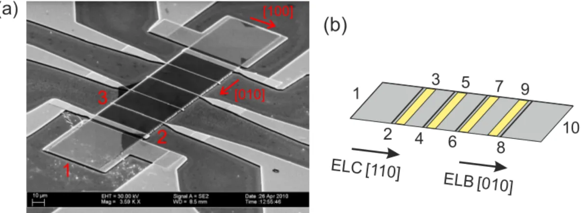
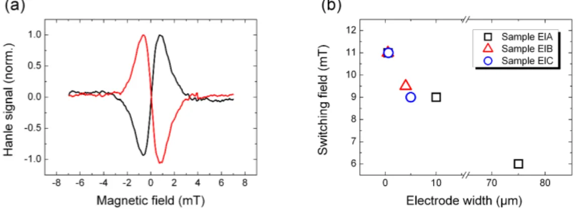
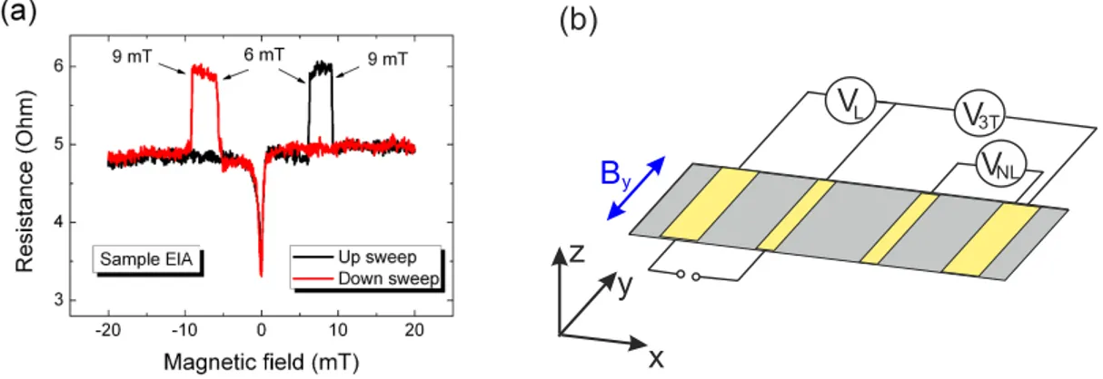
One part of the experimental results presented in this work is investigating such a structure. Spin dynamics and spin transport phenomena are examined employing the Hanle-MOKE technique. Similar samples have already been investigated with different detection methods and geometries: Ciorga et al. demonstrated an all-electrical spin injection and detection method [Cio09; Cio10; Cio11; Ein09], and Endres et al. used cross-sectional imaging of the spin polarization on the cleaved edge of the GaAs channel [End11; End12]. Together with these works, the results presented here give a more complete description of this kind of samples.
In the second part of this work, two-dimensional electron systems embedded in GaAs/
AlGaAs quantum wells grown on a (110)-oriented substrate are investigated. The special symmetry of (110)-grown quantum wells promises long spin lifetimes [Ohn99b; Ada01;
D¨oh04; M¨ul08]. Due to the use of very sophisticated growth schemes [Uma09], excep- tionally high electron mobilities are present in the samples examined here. Spin lifetimes of up to 248 ns at low temperatures were observed, employing RSA-measurements in one of the utilized samples [Gri12a; Gri12b]. Besides studying the spin dynamics under the influence of external parameters such as temperature, carrier density and excitation density, spin transport phenomena such as spin diffusion and spin drift are also exam- ined. The Hanle-MOKE method and photoluminescence measurements are the means for these investigations. Furthermore, current-induced spin polarization is demonstrated in the samples. This method of generating a spin orientation was already successfully demonstrated at room temperature in n-type ZnSe epilayers [Ste06]. Under the condi- tion that the spin polarization can be made large enough, this method has the potential to become an efficient tool to generate spin orientations in non-magnetic semiconduc- tors.
The structure of this work is as follows:
Chapter 2 outlines the fundamental theory. It starts with the material properties of GaAs, GaAs heterostructures, and the ferromagnetism in (Ga,Mn)As. Afterward, the
concepts of generating a spin imbalance in a semiconductor are elucidated, in particular electrical spin injection and optical spin orientation. Then this chapter discusses spin- orbit interaction in connection with crystal symmetries and the various spin dephasing mechanisms. Next subject are the transport phenomena such as diffusion and drift, which are discussed in regard to carrier and spin. The chapter closes by giving attention to dynamic nuclear polarization.
Chapter 3 explains the measurement techniques and the experimental setup. First, it illustrates the magneto-optic Kerr/Faraday effect and its combination with the Hanle effect, the technique most employed in this work to determine spin lifetimes and spin polarization. Then, this chapter discusses photoluminescence spectroscopy and the possibilities of changing the carrier density by gating optically as well as electrically.
Chapter 4 describes the experiments, in which a p+ (Ga,Mn)As/ n+ GaAs Esaki Zener diode structure is used to inject a spin polarization into GaAs bulk. First, the sample structure is described and characterized in terms of I-V characteristics and the dependence of the magnetization of the electrode on an external field. The spin lifetime in the sample is then investigated utilizing an all-optical method in comparison to the results from electrical injection. Then, the chapter focuses on the sign of the spin polarization depending on the applied bias at the electrode. By moving the detection laser spot on the sample relative to the spin injecting contact, spin diffusion and spin drift profiles are revealed. Finally, this chapter introduces a technique, where electrical and optical spin injection are combined in order to observe dynamic nuclear polarization effects.
Chapter 5 presents first the complex sample structure of the high-mobility (110)- grown quantum wells. For a complete description of the spin dynamics, knowledge of the carrier dynamics depending on the external parameters is essential. Therefore, this chapter introduces photoluminescence measurements as well as time-resolved photolu- minescence measurements. Then the spin dynamics for three samples, which differ in terms of quantum well width and carrier density, is examined in regard to the external parameters temperature excitation density and carrier density (modulated by above- barrier illumination). Hereby, spin-resolved PL measurements support the results of the Hanle-MOKE technique. Spin diffusion is investigated when varying the relative distance between injection point and detection point. The spin diffusion is monitored depending on an external gate voltage as well. In (110)-grown quantum wells, the sym- metry of the Dresselhaus field together with an electron drift, yields an out-of-plane spin polarization, owing to current-induced spin polarization. After this effect is examined the chapter focuses on further effects of electron drift, such as the reduction of the spin lifetime. Finally, dynamic nuclear polarization in this system is discussed briefly.
Chapter 6 presents the summary of the results.
Basics
The materials subject to investigation in this work are based on gallium arsenide and aluminium gallium arsenide, which have drawn quite some attention in semiconduc- tor physics in the past decades. Constant developments in fabrication now provide very pure crystal structures, allowing the observation of quantum effects, and give rise to very high carrier mobilities. A full understanding of the spin dynamics requires knowledge of the fundamental material properties as well. This chapter starts there- fore with a brief discussion on the material characteristics and the fabrication of such semiconductor structures. This introduction contains as well the diluted ferromagnetic semiconductor gallium manganese arsenide, which is used as a source of spin injection in chapter 4. Thereafter essential fundamentals of electron spin physics in semiconduc- tors are outlined (chapter 2.2). This discussion starts with possibilities to generate a spin polarization in semiconductors, emphasizing the two mechanisms this work uses, optical and electrical spin injection. A crucial point in understanding spin dephasing, which is the relaxation of a spin imbalance into its thermal equilibrium, is to understand the interaction of the orbital motion of an electron and its spin. After discussing the most prominent spin dephasing mechanisms in GaAs based heterostructures, the spin dynamics, particularly in the investigated types, GaAs bulk and (110)-grown GaAs / AlxGa1−xAs, are illustrated. Besides the spin dynamics, the spin transport is studied as well here. This chapter outlines, therefore, the transport phenomena diffusion and drift with regard to carrier transport, as well as spin transport. The chapter closes with the influence and interplay of nuclear and electron spins.
2.1 Material properties
In this section the basic properties of gallium arsenide and aluminium gallium arsenide (GaAs / AlxGa1−xAs) are introduced, starting by addressing the crystal growth, and continuing by giving attention to the electronic band structure in the GaAs crystal.
Thereafter the formation of heterostructures as well as the possibility of doping is dealt with. Finally, the ferromagnetism in the diluted magnetic semiconductor (Ga,Mn)As is addressed.
2.1.1 GaAs / AlGaAs structures
The III-V semiconductors gallium arsenide (GaAs) and aluminium arsenide (AlAs) are the basic materials for the structures examined in this work. An effective spin trans- port entails high carrier mobilities, which can be achieved by producing high purity
5
crystal structures. The Molecular-Beam Epitaxy (MBE) 1 is a method to fabricate such materials. A basic setup of a MBE chamber is depicted in figure 2.1 (a). Here, pure materials evaporate from effusion cells, which are set in a ultra-high vacuum (UHV 10−9 Pa) chamber. Due to the UHV, which is supported by cryogenic cooling shields (to freeze out impurity atoms), the molecules do not interact with each other until they eventually condense on a heated and rotating substrate. The slow deposition rate this method provides, allows epitaxial growth. This means the deposited layer is congruent to the substrate (assuming matching physical properties of substrate and the evapo- rated materials). Mechanical shutters control the relative fluxes out of the effusion cells, and the growth is monitored with the RHEED technique (reflection high energy electron diffraction). In a nutshell, MBE provides crystal structures with sharp layer boundaries, and negligible thickness variations of the layer [Cho81].
Figure 2.1: (a) Schematic layout of a MBE chamber. Taken from [Kas06]. (b) The GaAs zincblende structure consists of two fcc lattices (Ga,As) shifted by(1/4,1/4,1/4) a (lattice constant) along the space diagonal. Taken from [Kas06].
The crystal structure of the compound semiconductor GaAs consists of tetrahedral covalent bonds by each Ga (As) atom formed with four As (Ga) atoms2 3. Hence, the two interpenetrating fcc (face centered cubic) lattices of the two atom types are forming a zincblende crystal as figure 2.1 (b) depicts. The space group symmetry of this crys- tal is symorphic and labeled Td2 [Dre55], with a space group number two, and a point group symmetry Td (similar to the methane molecule (CH4)). Td contains 24 symme- try operations: the identity, eight C3 operations (rotation by 120◦, two C2 operations (rotation by 180◦), sixS4 operations (rotation followed by a reflection perpendicular to the rotation axis), and six σ operations (reflection with respect to a plane) 4.
The energy of an electron moving in a crystal can only have certain energy values.
An exact calculation of this energy bands is quite complex, since the electron lattice interactions create a many-body problem. Thus, approximative models are necessary to determine theband structure. One of these is the intuitive tight-binding picture, where the valence orbitals of neighboring atoms hybridize (sp3 hybridisation) and form bonding and antibonding composite orbitals. Those composite orbitals broaden into bands because of the overlap of the orbitals in the crystal. On the one hand the s- antibonding orbitals (the angular momentum of the electrons is l= 0) form the lowest conduction band (CB), and on the other hand, the p-bonding orbitals (the angular
1Invented at Bell Laboratories [Art68; Cho71].
2 In the particular case of GaAs where two atom types are involved, additionally ionic bonding is present, resulting in a increased bond strength.
3Standard textbooks [Ash76; Kit96] describe the basic principles of chemical bonds.
4A detailed discussion of the symmetry groups may be found in [Yu05].
momentum of the electrons is l= 1) constitute the highest valence band (VB). Due to its s-like (l = 0) character the conduction band is double degenerate (spin degeneracy s = ±1/2), whereas the valence band has a six-fold degeneracy because of its p-like character. Furthermore, this degeneracy splits into a four-fold (heavy-hole HH and light-hole LH) and a two-fold degenerate band (split-off-band) as a result of the spin- orbit interaction (SOI )(see chapter 2.2.2). The terms heavy-hole and light-hole band are derived from their different effective masseswhich correspond to the curvature of the bands m1∗
i,j = 1
~2
∂2En(k)
∂ki∂kj . For bulk GaAs those two bands are degenerate at the Γ- point (k= 0), in heterostructures however this degeneracy is lifted (see chapter 2.1.1).
Figure 2.2 (a) exhibits the band structure of bulk GaAs close to the Γ-point, where an approximately parabolic behavior is assumed (effective mass approximation). The bands are occupied according to the product of the density of states and a distribution function, typically the Fermi-Dirac distribution. In that case the energy of the highest occupied state is called Fermi energy (EF). The position of the Fermi energy depends on factors such as doping concentration and the temperature 5. In 3D it may be expressed as: EF = [~2/(2m∗)](3π2n)2/3 and in 2D as: EF = ~2πn/m∗ [Gru06]. A couple of important expressions are derived from the Fermi energy: The Fermi temperature TF is defined as: TF = EF/kB, the Fermi velocity vF is given by: vF =p
2EF/m∗, and the Fermi wave vector kF is defined as: kF = (3π2n)1/3 in 3D, andkF =√
2πnin 2D.
Figure 2.2: (a) Band structure close to the Γ-point according to effective mass ap- proximation. Due to SOI the VB states split into states with total angular momentum j = 3/2 (HH-band, LH-band) and j= 1/2 (split-off band, SO-band). The difference be- tween the CB minimum and the VB maximum is the band gap energy Eg . The energy gap ∆0 is called the spin-orbit gap (SO-gap). Taken from [Win03]. (b) Band structure for GaAs. The top of the filled VB is set to zero energy. Taken from [Yu05].
A conceptually different approach to obtain the band structure is the quasi-free par- ticle approximation. Here nearly free valence electrons are considered, moving in a periodic potential of the ions and core electrons. In order to solve the one electron Schr¨odinger equation in such a periodic potential, Bloch’s theorem is used. The elec- tron wave function then has the form ψn,k(r) = un,k(r) exp[ik·r], with a periodic function un,k(r) and an envelope function exp[ik·r] 6. Nowadays very sophisticated methods are deployed to calculate band structures, such as the k·p-method. This
5Providing an undoped sample, the VB is fully occupied at zero temperatureT = 0, whereas the CB is not occupied at all. The Fermi energy is then located midmost between CB and VB.
6A detailed discussion may be found in standard textbooks like [Ash76; Kit96].
approach is based on the fact that the Bloch-function ansatz yields a coupling term
~k·~p in the Hamiltonian. Treating this k·p-term as a perturbation, the energy band structure is calculated. Considering the degeneracy of the VB, however, spin orbit in- teraction must be included, and the incorporation of higher order perturbation terms are necessary. Usually it is sufficient for an effective calculation to consider the bands Γ6,Γ8 and Γ7. This is called the Kane model7. A further approach is the pseudopoten- tial method, where the strong Coulomb potential of the nucleus and the core electrons are replaced by an effective ionic potential acting on the valence electrons. The band structure displayed in figure 2.2 (b) is a result of pseudopotential calculations. Detailed discussions on such methods may be found in [Win03; Yu05]. It is often sufficient to consider only the states close to the Fermi energy or at the minimum of the conduction band. For small k, the band around the minimum can be approximated as parabolic.
Using a Taylor expansion up to second order and assigning the second derivative to an inverse effective mass (m∗e,h) allows the use of a semiclassical model of transport.
Corrections due to high order effects may invoke non-parabolicity though. Since each band has a unique curvature that is reflected in the effective mass, this approximation is called effective mass approximation (figure 2.2 (a)). Strictly speaking, holes in the Γ8-band cannot be described by such an effective mass approximation since they are highly anisotropic and nonparabolic.[Win03].
Heterostructures
Crystal growth techniques, like the MBE method, allow the fabrication of ternary alloys such as AlxGa1−xAs. In such structures one of the two above mentioned fcc-lattices consists of As atoms and the other is statistically occupied by Ga and Al atoms. Because AlAs has a larger bandgap than GaAs, the band gap of the alloy may be designed, by changing the portion of Alx (Eg = 1.424 + 1.247x[eV] at room temperature [Lev99]).
Since the emission/absorption lies in the near IR to red spectral range, this material is quite interesting for optoelectronic applications. However, only in the range 0 < x <
0.45 AlxGa1−xAs has a direct band gap, i.e., the maximum of the highest valence band and the minimum of the lowest conduction band are at the Γ-point (k=0), see figure 2.2. For 0.45 < x < 1 the conduction band minimum can be found at the X- point, yielding an indirect band gap, see also chapter 2.2.1. The width of the band gap depends on the temperature as well, since an increase in temperature causes an expansion of the lattice, due to a rising amplitude of atomic vibrations 8. According to the Varshni formula the maximal band gap energy Eg at T = 0 K decreases first quadratically (T ΘD 9) and changes into a linear decline for higher T [Var67]:
Eg(T) =Eg(T = 0)−αvT2/(T+βv). (2.1) Hereαv represents the volume coefficient of thermal expansion andβv the volume com- pressibility. Thus, in the direct band gap regime, the band gap energy of AlxGa1−xAs for low temperatures, is given by [Lev99]:
Eg = 1.519 + 1.155x+ 0.37x2[eV]. (2.2) Standard textbooks and publications such as [Ada85; Kas06; Lev99] also include further fundamental material properties.
The nearly identical lattice constants of GaAs and AlAs (a = 5.6533 + 0.0078x[˚A]
allow a strain-less growth of relatively thick AlxGa1−xAs layers. One may create het- erostructures with various potential landscapes, like a potential well, by stacking such
7There exists also an extended Kane model which includes 12 bands.
8Strictly speaking only due to the anharmonic potential.
9ΘD Debye temperature.
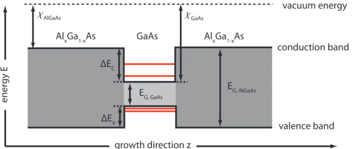
layers with different band gaps. The structures this work uses are categorized as type I, where the higher VB edge and the lower CB edge are both in the material with the smaller bandgap. These offsets of CB and VB are calculated from the difference of the electron affinities (χ) in the materials10 (see figure 2.3). In the case the de Broglie wavelength is comparable with the layer thickness d 11, the electron and hole states along the growth direction z12are quantized in so-called subbands (see figure 2.3). The
AlxGa1-xAs GaAs AlxGa1-xAs
AlGaAs GaAs
EG, AlGaAs EG, GaAs
ΔEC
ΔEV
conduction band
valence band vacuum energy
energy E
growth direction z
Figure 2.3: Type-I heterostructure. The CB and VB discontinuities are given by∆EC = χAlGaAs−χGaAs and ∆EV = (χAlGaAs +EG,AlGaAs)−(χGaAs+EG,GaAs) are given.
Taken from [Gri12b].
electron/ hole states are stationary in this direction, along the in-plane axis the Bloch wave character remains though. In such a 2D-electron-system (2DES) the density of states is now a step function (in 3D it is proportional toE1/2). One speaks of a quantum well (QW) in the case of confinement in a single direction, whereas for two (three) con- finement directions a quantum wire (quantum dot) is present. A further consequence of the confinement of electrons and holes is the increase of the radiative recombination probability. In order to estimate the confinement energy, it is often sufficient to consider a model of a potential well with infinite high barriers, where the allowed electron wave vectors in z direction are given bykz,n0 =n0π/d, and the electron energy is given by:
En0,k=En0,kz +En0,kk = ~2 2m∗e,h
"
n0π d
2
+kx2+ky2
#
. (2.3)
Here n0 is the subband index, kk the in-plane component of the k-vector, d the QW width and m∗e,h the electron/hole effective mass. Assuming a finite potential barrier height allows the electrons to tunnel into the barrier. The electron wave function decays exponentially in the barrier, and the eigen-energies are reduced compared to those of the infinitely deep well 13. Within the well, the electron wave functions are approximately sinusoidal and have parities of (−1)n0+1 (n0 = 1,2, ... subband index).
The envelope function approximation, which is based on thek·p-method, is often used to calculate the band structure of heterostructures [Bas81]. Herein the wave functions
10This so-called Anderson rule may, however, only be considered as a qualitative approximation [Bau83].
11λdB=h/√
2πmkBT. For an estimate, one can consider for an electron in GaAs an effective mass ofm∗= 0.067me(k= 0) [Ada85]. Hence atT = 4 K a layer thickness of 144 nm would be sufficient to see quantized effects.
12In the following a cartesian coordinate system x,y,z is used with z being the growth direction
13Examples may be found in [Bas81; Bas85; Yu05].
are a product of fast oscillating Bloch functions and a slowly varying envelope function in the corresponding region of the heterostructure. Such calculations show that in 2D the size quantization lifts the degeneracy for the HH and LH bands at the Γ-point.
Moreover, the HH and LH bands have a reversed correlation in the plane than along the quantization axis, yielding a coupling between HH and LH states for k 0. This HH-LH mixing gives rise to a repulsive behavior of the two bands, the so-called HH- LHanticrossing, where the light hole and heavy hole character (band curvature) are exchanged (see figure 2.4 ).
In addition to the band structure theory, the interac-
Figure 2.4: Scematic pic- ture of HH-LH anticross- ing [Win03].
tion of free carriers is important in semiconductors. Due to the Coulomb interaction between electrons and holes, a bound state, a so called neutralexciton, is formed14. Ex- citons may be described analogously to a hydrogen model with discrete states below the bandgap energy, leading to an optical absorption below the bandgap, for more details see [Gru06; Yu05; Dya08]. In quantum wells, electron and hole wave functions overlap more because of the spatial confinement, yielding an increased binding energy for ex- citons compared to the bulk. For large electron densities, these excitons are not stable though, because the screening effects reduce binding energy.
Doping
The occupation of the bands is defined by the product of the density of states and the step-like Fermi-Dirac distribution: fe(E) = 1/(exp [(E−EF)/kBT] + 1) with EF
the Fermi energy. For E −EF >> kBT this function can be approximated by the Boltzmann distribution: fe(E) = 1/(exp [(E−EF)/kBT]). In this case, the system is called nondegenerate (high T or small carrier density), otherwise the system is called degenerate (smallT or high carrier density). If the Fermi level is within the band, the system is highly degenerate [Gru06]. In order to increase electrical properties, such as conductivity, the carrier concentration (electrons or holes) is intentionally increased by introducing impurities. III-V semiconductors are usually doped with materials of the IV group, typically C, Si. The temperature of the effusion cells in the MBE controls in which sublattice the doping atom is integrated and thereby whether the atom acts as donor or acceptor. Low-doped semiconductors obey nondegenerate statistics, whereas highly-doped semiconductors follow degenerate statistics (like metals).
Additionally to its effect on spin dephasing (discussed in section 2.2.4), the doping concentration has a strong influence on the optical absorption edge (see also section 2.2.1). On the one hand, because of the resident electrons in the CB owing to n-doping, higher energies are required to lift an electron from the VB into an unoccupied state in the CB. This shift in the absorption energy is called the Burstein-Moss shift ∆BM
[Mos54; Bur54]. On the the other hand, exchange and Coulomb interactions between the additional electrons as well as electron impurity scattering, lead to a reduction of the band gap, which is called band gap renormalization ∆RN [Wal08; DS90; Kle85b].
Hence, the net change in the bandgap energy ∆Eg is ∆Eg = ∆BM −∆RN.
Although large carrier densities are essential for high mobilities, the ionized impurity atoms induce scattering, which reduces the carrier mobility. Heterostructures, however, provide the possibility to integrate the doping into the barriers (remote doping). The carriers diffuse into the energetically favored quantum well, and due to the spatial separation, scattering of electrons and doping atoms is reduced. Nevertheless, remote donor scattering (scattering via Coulomb interaction) still exists, which needs to be
14If an additional electron or hole is involved one speaks of a negatively or positively charged exciton.
suppressed by the incorporation of an additional undoped layer. Such a procedure is called modulation doping [Din78; Dru81]. The ionized donor concentration in the wide bandgap material and the electron concentration adjacent to the heterointerface introduce a built-in electric field (through Poisson’s equation E = −∇φ with φ the electrostatic potential). This dipole layer gives rise to an equilibrium band bending. A single-sided doping (ssd) causes therefore the electron wave function to shift towards the doped layer and to penetrate deeper into the low mobility barrier material, which reduces the total mobility 15. Thus, in order to achieve high electron mobilities double- sided doping (dsd) is employed. Using highly sophisticated growth schemes [Uma09]
may achieve further enhancement, see also chapter 5.1 for more details. Additionally, a symmetric band profile is also essential for long spin lifetimes (see chapter 2.2).
2.1.2 Ferromagnetism in Gallium manganese arsenide
For the electrical spin injection discussed in chapter 4, a ferromagnetic contact com- posed of gallium manganese arsenide (Ga,Mn)As, introduces a spin polarization into GaAs bulk. Such an all-semiconductor device bears some advantages (described in chapter 2.2.1) compared to a combination of a ferromagnetic metal with a semiconduc- tor. In a typical semiconductor like GaAs no magnetic order is present (diamagnetism may still exist). Furdya et al., however, proposed the doping of semiconductors with magnetic transition metals, yielding so-called diluted magnetic semiconductors (DMS) [Fur88]. DMS are an alloy between nonmagnetic and magnetic semiconductors16where the magnetic moments are randomly distributed in the host. (Ga,Mn)As 17, a DMS on the basis of the widely used semiconductor GaAs, was introduced by Ohno et al.
[Ohn96; Ohn98]. In this material, the Mn atoms substitute ideally a Ga atom in the lat- tice. Although less likely, the Mn atoms may also be incorporated interstitially, meaning the Mn atom sits between the atom sites in the lattice. There are different possibilities for a Mn atom to incorporate into the lattice: two tetrahedral positions between four As/Ga atoms (TAs4, TGa4) or hexagonal positions between three As/Ga atoms. Yet TAs4 is energetically favored [Maˆs04; Hol06]. The crystal structure of (Ga,Mn)As with both (substitutional, interstitial) incorporation cases is depicted in Figure 2.5 (a). In the crystal, substitutional manganese acts as an acceptor, since Mn has an electron less than Ga in the 4p shell (Mn = [Ar] 3d54s2, Ga = [Ar] 3d104s24p1). This acceptor behavior, however may be compensated partially (even fully), due to interstitial Mn impurities, which act as double donors, owing to the two 4s2 electrons. The 3d shell of a Mn atom is only half occupied, yielding a magnetic moment of 5/2µB according to Hund’s rules [Lan77]. Since these electrons are not involved in the atomic bonding, the magnetic moment is conserved in the macroscopic material, bearing ferromagnetic behavior. Typically, the MBE growth temperature for GaAs is high (∼ 600◦ C), to ensure a pure crystal growth. The low solubility of Mn in GaAs, however, would cause segregation at this high temperature, yielding a Mn accumulation on the surface. There- fore, low temperatures are necessary on the one hand to incorporate the Mn atoms, but on the other hand, are giving rise to the implementation of defects. Eventually, the combination of growth temperature and the Mn concentration determines the state of the alloy. The phase transitions of the alloy depending on growth temperature and Mn concentration are depicted in figure 2.5(b). At low temperatures a transition from
15Typically one distinguishes in ssd heterostructures on which side of the GaAs layer the doping is introduced. In a normal heterostructure the doping is on top of the GaAs layer. Is this on the contrary the other way around one speaks of a inverted heterostructure. Although an inverted structure allows a better formation of an ohmic contact, the electron mobility is lower due to dopant migration in growth direction [Sht88].
16Magnetic semiconductors like MnAs contain a sublattice with magnetic elements.
17The notation according to section 2.1.1 Ga1−xMnxAs is also often used.
Figure 2.5: (a) Crystal structure of (Ga,Mn)As. Defects in the crystal structure are for example As anti-sites AsGa. MnI represents a Mn interstitial. Taken from [Mac05].
(b) Schematic phase diagram showing the properties of (Ga,Mn)As, grown by MBE, depending on substrate temperature and Mn concentration. Taken from [Ohn98].
the insulating to the metallic phase happens with rising Mn concentration, whereas for very high temperatures and high Mn concentrations (metallic) MnAs crystallizes in a NiAs-structure [Ohn98]. The growth of the desired metallic (Ga,Mn)As requires low temperatures (∼ 230◦ C to ∼ 260◦ C) and a Mn concentration of 2% to 6%. The drawback of the low temperature growth is the inclusion of further impurities like Ga vacancies (not occupied Ga site, acts as acceptor) or As antisites (As on a Ga site, acts as double donor, AsGa) in the crystal.
Below the Curie temperature (TC) ferromagnetic materials have a nonvanishing spon- taneous magnetization M, even in the absence of an external magnetic field. In this regime the magnetic moments are oriented parallel within domains, and an external magnetic field may align the magnetization directions of the domains macroscopically.
Above TC on the contrary, the magnetic moments are randomly oriented in the para- magnetic phase. In a phenomenological description of ferromagnetism, the magnetic moments align in such a way that the total energy consisting of the exchange energy and the kinetic energy is minimized, yielding an energy splitting in the density of states of the two spin orientations, see figure 2.6. A simple model to describe ferromag- netism is the Heisenberg model. In this approach the two nearest neighbor spins couple (anti)ferromagnetically according to the Heisenberg Hamiltonian:
Figure 2.6: The density of states for the two spin orientations is split in the energy for a ferromagnet.
Taken from [Pri98].
HˆH =−X
i,j
J˜i,jSi·Sj, (2.4) whereSi,j are two nearest neighbor spins and ˜Ji,j
is the exchange integral 18. There are various kinds of exchange interactions. In the common 3 d transition metals for example, the ferromagnetism is based on the direct exchange interaction, which is an interplay between the Coulomb interaction and the Pauli principle 19. In (Ga,Mn)As, due to the dilute incorporation, the average distance of magnetic moments is too large to allow for a di-
rect exchange coupling, since the overlap of the wave functions of the involved spins is
18The sign of ˜Ji,j defines the type of the coupling: ˜Ji,j <0 means antiferromagnetic and ˜Ji,j >0 means ferromagnetic coupling
19[Blu01; St¨o06] for example, include a detailed discussion of ferromagnetism.
too small. Nevertheless, Ohno et al. observed a ferromagnetic order in (Ga,Mn)As for Mn concentrations higher than 1% [Ohn96; Ohn98], indicating that the ferromagnetism in (Ga,Mn)As is caused by an indirect exchange interaction, the so-called RKKY (Rud- ermann, Kittel, Kasuya, Yosida [Rud54; Kas59; Yos57; Blu01; St¨o06]) interaction based on itinerant holes. A magnetic impurity within a metallic material is screened by the itinerant carriers. In this process, the carriers get spin polarized and can couple with other close-by magnetic moments 20. The resulting exchange integral in equation 2.4, in the case of RKKY interaction, has an oscillatory behavior: ˜Ji,j ∝ cos(kFri,j)/ri,j3 withkF the Fermi wave vector andri,j the distance between the two coupled magnetic moments.
For the metallic (Ga,Mn)As, with Mn concentrations of 1−12%, the distances are small enough to assume only antiferromagnetic coupling [Jun06]. Thus, the holes couple antiferromagnetically with the localized 3d electron spins (p-d interaction), yielding a local ferromagnetic coupling between two Mn magnetic moments. In the case the hole concentration is large enough, the hole impurity band merges with the GaAs valence band, and the holes, that are now freely propagating, align the Mn spins all over the sample. Dietl et al. [Die00; Die01] developed a mean-field Zener model to describe the ferromagnetism in (Ga,Mn)As in detail. In this approach the p-d interaction is considered as an effective magnetic field which causes a spin splitting in the valence band. Below the Curie temperature, it is energetically more favorable to align the Mn spins than to redistribute the holes. The expression found for the Curie temperature is:
TC ∝xin1/3h , (2.5)
with nh the hole concentration and xi the effective Mn concentration 21. Compared to the magnetic 3d materials, the Curie temperature in (Ga,Mn)As is lower, since the indirect exchange coupling is weaker than the direct exchange. A high Mn concentra- tion, as well as a high hole concentration, is necessary in order to achieve high Curie temperatures. This, however, requires low growth temperatures, yielding the incorpo- ration of impurities which again may compensate the p-doping, that is essential for the ferromagnetic coupling. The initial Curie temperatures of 60 K to 110 K [Mat98] could be topped by including post-growth annealing processes 22[Hay01; Edm02; Pot01], and Curie temperatures up to 173 K were reported [Wan05a; Jun05]. Recently it was shown that (Ga,Mn)As nanostructures may have a Curie temperature of up to 200 K [Che11].
Maccherozzi et al. found a robust magnetic coupling between a thin Fe film epitax- ial grown on top of an undoped (Ga, Mn)As (100) layer. Thus, in the paramagnetic (Ga, Mn)As, ferromagnetic proximity polarization induces ferromagnetic order. This approach could produce a stack of Fe/(Ga, Mn)As thin layers with a Curie temperature up to room temperature.
2.2 Spin in Semiconductors
Electrons carry an intrinsic form of angular momentum called spin [Uhl26]. Although such a spin can point in any direction, according to the uncertainty relation, only one component can be measured at a time, giving two possible eigen-valuessi =±~/2 (i= {x, y, z}). The associated magnetic moment ¯µi =−g0µBsi/~is antiparallel to the spin angular momentum. Hence, the ratio of the spin angular momentum and the magnetic moment (also gyromagnetic ratio) is characterized by the Bohr magnetonµB=e~/2me
20An equivalent phenomenon based on electric charges in metals are the Friedel oscillations [Fri54].
21A review of further properties of (Ga,Mn)As may be found in [Jun05].
22After the MBE growth the sample is heated. Thus, the weakly bound defects like As antisites or Mn interstitials are thermally activated and diffuse to the surface, leading to a purer crystal structure.
and a dimensionless quantity, the so called g-factor g0, also called gyromagnetic factor or Land´e factor. From the Dirac equation a value ofg0 = 2 for a free electron is derived.
Quantum electrodynamics, however, provides a correction ofg0 = 2 (1 +α0/2π+...)≈ 2.0023 (with α0 = e2/(4π0)~c fine structure constant) [Sch00b; Sch48; Odo06]. In a semiconductor crystal the electron g-factor may deviate from the vacuum value due to the influence of the spin-orbit interaction, see chapter 2.2.2 for a detailed discussion.
The quantum state of a spin-1/2 particle is described by a normalized two-component vector (spinor) in Hilbert space, and the corresponding spin operators are represented by 2×2 matrices, the Pauli matrices ˆsi = (~/2) ˆσi. In a nonmagnetic semiconductor at equilibrium the spins are statistically oriented. Various methods discussed in section 2.2.1 can be applied to create a surplus of one “spin kind”. Such a degree of spin polarization is given by:
P = n↑−n↓
n↑+n↓
, (2.6)
where n↑↓ represents the carrier density of the two spin types. One distinguishes the degree of spin polarization from the spin polarization, which is defined as oriented non equilibrium spins per area in a 2D system or spins per volume in bulk:
PS =P ·n, (2.7)
with n the carrier density, which is the number of spins per area N/A or per volume N/V˜.
In the following, means to induce such a spin imbalance in a semiconductor are pre- sented, succeeded by the introduction of spin-orbit interaction (SOI) 2.2.2. SOI not only has an impact on the magnetic moment and the electron g-factor, but is also respon- sible, with the crystal symmetry, for breaking the spin-degeneracy. After establishing the general terms of spin dynamics, spin relaxation and spin dephasing in section 2.2.3, the spin dephasing mechanisms important for this work are presented in section 2.2.4.
This chapter closes with a discussion on the special case of (110)-grown quantum wells 2.2.6.
2.2.1 Generation of a spin polarization
In a nonmagnetic semiconductor the spins are statistically oriented, in a way that spin up and spin down orientations are balanced. Finding an effective manner to create a spin imbalance has been a great effort in science recently. In this work, the spin injection is done optically with a circularly polarized laser, and electrically using a ferromagnetic (Ga,Mn)As electrode. Both methods are introduced in the following.
There are, however, other means to create a spin imbalance. One example is the Spin Seebeck effect, where spin imbalance arises due to a thermal gradient [Uch08]. Another viable method is the Spin Hall effect, which is based on the fact that an electrical current driven through a material with a strong spin-orbit interaction yields a spin imbalance at the edges of the conducting channel [Dya71b; Dya71a; Kat04b].
Optical spin injection
The interaction of light with a semiconductor crystal may be described similar to the interaction of light with a single atom, providing a symmetry, that is high enough for an isotropic momentum distribution of electrons and holes. Typically, the transition probabilities between two states are given by Fermi’s golden rule, which is derived by solving the time-dependent Schr¨odinger equation [Sch00b]:
T˜i→f = 2π
~ X
f
|hf|Vf i|ii|2δ(Ef −Ei±~ω), (2.8)
with hi| and |fi the initial and final states and Vf i the perturbation operator. The delta function term indicates the conservation of energy, where an incident photon creates an electron-hole pair in conduction and valence band for ~ω ≥ Eg. Since the momentum of the photon is evanescently small compared to the electron momentum, the momentum transfer due to the conservation of momentum is neglected (pe−ph = h/λ ≈ 0), implicating a vertical transition in k-space (ke ≈kh). In first order, Vf i is approximated by an electrical dipole potential. The possible transitions are constrained by selection rules obtained in first order through the electric dipole approximation. In the limit of weak SOI, the electric dipole operator does not depend on the spin. Hence, the conservation of angular momentum in interband transitions leads to selection rules for the total angular momentum J = 0,±1 and its projection on the quantization axis (magnetic quantum number) mJ = ±1 23. These selection rules are satisfied by left (σ+) or right (σ−) circularly polarized photons incident along the quantization axis, since they carry an angular momentum s= 1 with mph =±1. The relative transition probabilities, for σ±-light, are derived from the matrix element in equation 2.8, and are depicted in figure 2.7 (a), for σ+-light in the case of GaAs-bulk. An excitation from all three valence bands would therefore imply no spin polarization. A spectrally narrow excitation, leaving out the split-off band, however, results in a spin polarization of 50% according to equation 2.6 (P = (3−1)/(3 + 1) = 0.5). As discussed in chapter 2.1.1, the spatial confinement in a quantum well lifts the degeneracy of the HH and LH-bands. In the case that the spectral width of the excitation is small enough, and only electrons from the HH-band are excited, a spin polarization of 100% is achieved (figure 2.7 (b)). According to the conservation of angular momentum, for incident light along the quantization axis, the generated spin imbalance is oriented along the sample normal. Certainly, these selection rules are valid for emission as well, see chapter 3.3.
In (modulation) doped quantum wells, resident electrons occupy the states up to the
Figure 2.7: (a)Transition probabilities for σ+-light, in GaAs-bulk at the Γ-point. As shown in chapter 2.1.1, GaAs has a direct bandgap with aΓ6 conduction band and aΓ8
valence band. (b) In a Quantum well, spectral narrow excitation can produce full spin polarization, due to the HH-LH splitting. Taken from [Kor10].
Fermi energy, which is in a 2DES represented by a Fermi disc in k-space. Optical excitation is only possible for wave vectors around the Fermi disc (see figure 2.8). The admixture of HH and LH states in the VB fork>0 (chapter 2.1.1) results in excitation of both spin orientations, yielding reduced net spin polarization [Pfa05]. Thus, equation 2.6 is modified to [Kor10]:
Pred= nopt
ne+ntotopt, (2.9)
23In quantum wells, the different parity of the envelope function implicates the selection rule ∆n0= 0 in case of infinite barrier height, otherwise ∆n0 = 0,2,4, ...withn0 the subband index. This condition can be lifted due to asymmetries, e.g. the different effective masses of electrons and holes cause a not equal penetration of the wave functions into the barrier materials.
k
xk
yk
Fk
xk
yk
FFigure 2.8: Optical orientation in a 2DES. In doped quantum wells, resident electron occupy states up to the Fermi wave vector kF. Optically excited states are around the Fermi disc. The spin polarization is parallel to the quantization axis. Taken from [Gri12b].
with ntotopt is the total optically created electron density, ne the density of the resident electron andnopt =ξ·ntotopt the spin polarized portion ofntotopt. Because of the admixture of HH and LH band and the scattering between them, the spin polarization of the optically created holes dephases very quickly. Usually, this dephasing takes place on the scale of the momentum scattering time, which is below the photocarrier recombination time. Therefore, the holes recombine as well with background electrons leaving a spin polarization in the resident electrons. The optically created electron density within the laser spot can then be approximated as follows:
ntotopt = 0.86
πr2 ·α˜ab· P λ/hc¯
·τph. (2.10)
The first term describes the effective illuminated area of a gaussian beam profile. ˜αab is the absorption coefficient. The third term describes the photon number per second with ¯P average laser power andλthe laser wavelength. τphis the photocarrier lifetime.
An asymmetry in the quantum well reduces the absorption energy due to the quantum confined Stark effect, and the overlap of the electron and hole wave function is decreased causing a lowering of the recombination efficiency[Mil84].
Electrical spin injection
The concept of a spin field effect transistor (sFET) Datta and Das proposed [Dat90]
raised great research interest in how to inject a spin polarization electrically, from a ferromagnet into a semiconductor. The discussion in this section starts by examining the spin polarization in the ferromagnetic contact and at the interface with a semiconductor in general, and continues focusing on the case of the p+ (Ga, Mn)As/ n+ GaAs Esaki Zener diode structure, which is used as a spin injection device in chapter 4.
In a ferromagnetic material the two spin subbands are split in energy, because of an exchange interaction, as described in section 2.1.2. Therefore, the densities of states (DOS) at the Fermi energy differ for the two spin orientations, yielding a strong impact on the mobilityµ(see chapter 2.3.1) for those two spin kinds, since the scattering takes place at values around the Fermi energy. The total current through a ferromagnet can be described by the two current model proposed by N.F. Mott [Mot64; Fer68], where the two spin species are described by independent currents with different mobilities.
Thus, the current spin polarizationPj, caused by the split in the Fermi energies, can be described analogously to equation 2.6. In general this value is different from the density spin polarization P degree though. For a homogenous nonmagnetic semiconductor, the relation betweenPj and P is given by[Yu02b]:
Pj(x) = j↑−j↓
j↑+j↓ =P(x) + D µE ·dP
dx, (2.11)
with D the diffusion constant, µ the mobility, and E the electric field. Moreover, a current density can be defined in the ferromagnet F and in the non magnetic material N by:
jF,N = ˜βF,NjF,N↑ +
1−β˜F,N
jF,N↓ . (2.12)
The parameter ˜βF,N is a dimensionless parameter indicating the asymmetry of the current (in equilibrium: ˜βN = 0.5). Pj at a ferromagnet/nonmagnet interface (F/N) is often called spin injection efficiency, and is given by: Pj = 2 ˜β−1 [St¨o06]. Since charge neutrality requires a constant current density across the F/N interface, the different current densities on each side adjust to the interface value. The electrochemical potential
˜
µ 24 splits, therefore, for up and down spins at the interface. Hereby spin flips are induced (majority spins transform into minority spins) and a spin accumulation at the interface occurs ˜µs = ˜µ↑−µ˜↓ [Val93; Cha07b], which implicates a nonequilibrium magnetization in the nonmagnetic material, see figure 2.9. Such a spin accumulation
˜
µs obeys a spin diffusion equation ∇2µ˜s = ˜µs/L2s [Son87; Val93; Fer01; ˇZut04], where the spin diffusion lengthLF,Ns depends on the spin relaxation rate (described in chapter 2.2.4) of both the ferromagnet and the non magnetic material. In case of a transparent contact, meaning without an interface resistance, the spin accumulation is equal on both sides of the interface and decays exponentially [Fer01; Jaf02].
Figure 2.9: (a) Interface between ferromagnet and nonmagnet. The chemical poten- tials µ˜↑,↓ for spin up and spin down are discontinuous in the case of a small interface resistance. This allows for an efficient spin injection. In the case of a transparent in- terface, on the contrary, µ˜↑,↓ would be continuous and the two diffusion lengths LsF,N
are equal, and for a common spin polarization of a ferromagnet no effective spin injec- tion is possible. The discontinuity of the averaged chemical potentials is called the spin accumulation voltage ∆˜µ. Taken from [ ˇZut04]. (b) The width of the zone of the spin accumulation is determined by the spin diffusion length LsF,N. The spin polarization Pj decreases continuously from the ferromagnet to the nonmagnet. The huge difference in the conductance between metal (M) and semiconductor (SC) causes almost the whole spin polarization to relax before the interface. Adapted from [Cha07b].
24The electrochemical potential is defined as the change in the energy in a thermodynamical system if an additional particle is added. For T = 0 it is identical to the Fermi energy, and even at room temperature the Fermi energy is a good approximation for the chemical potential. A general expres- sion is: ˜µ = EF
1− π2/12
·(kBT /EF)2
. The current densities can be expressed in terms of the electrochemical potential with Ohms law: j↑,↓= ˜σ∇˜µ↑,↓(with ˜σthe conductivity) [St¨o06].