transport characterization of doped graphene
I n a u g u r a l - D i s s e r t a t i o n zur
Erlangung des Doktorgrades
der Mathematisch-Naturwissenschaftlichen Fakultät der Universität zu Köln
vorgelegt von
Herr Dipl.-Phys. Martin Gordon Hell aus
Rosenheim
Köln, 2019
Prof. Dr. Klas Linfors
Vorsitzender: Prof. Dr. Achim Rosch
Tag der letzten mündlichen Prüfung: 15.07.2019
1.6 Transport properties of graphene . . . 19
2 Publications 21
2.1 Resonance Raman spectrum of doped epitaxial graphene at the Lifshitz transition . . . 21 2.2 Origin of the flat band in heavily Cs doped graphene . . . 34 2.3 Combined ultra high vacuum Raman and electronic transport
characterization of large-area graphene on SiO2 . . . 72
3 Further publications 79
3.1 Facile preparation of au(111)/mica substrates for high-quality graphene nanoribbon synthesis . . . 79 3.2 Semiconductor-to-Metal Transition and Quasiparticle Renormal-
ization in Doped Graphene Nanoribbons . . . 84
4 Bibliography I
5 Abstract V
6 Zusammenfassung VII
1.1 Purpose of this thesis
The spectroscopic and electronic characterization of air-sensitive two-dimen- sional materials is a scientific and technical challenging task. This thesis is mo- tivated by the investigation of the Raman response of heavily doped graphene using a ultra-high vacuum (UHV) Raman spectrometer in tandem with the characterization of the graphene band structure if the Fermi level approaches the saddle point of the van Hove singularity using photoemission spectroscopy.
A further motivation is the electronic characterization of pristine and doped graphene. This required the realization of an experimental setup for electronic transport measurements in ultra-high vacuum, which is shown in this thesis.
We started to dope epitaxially grown graphene on Ir(111) with Cs and com- bined in-situ Raman spectroscopy in tandem with angle-resolved photoemis- sion spectroscopy (ARPES) to describe the modification of the electronic band structure. By analyzing the evolution of the doping-dependent Raman spec- trum from pristine epitaxially grown graphene to a heavily Cs doped state, we were able to establish a fully experimental relation between the energy shift and Fano [4] asymmetry parameter of the Raman G band versus carrier concentration obtained by ARPES[Chapter 2.1]. The energy shift could be explained by the effects of phonon renormalization due to the removal of the Kohn anomaly [5] and the lattice expansion [6], resulting in a phonon upshift and downshift respectively.
Further doping led to a new technique for inducing a flat band in the band
alkali metal (Cs) layers. The obtained trilayer system was investigated by ARPES and we could explain the origin of the doping induced flat band at the M point of the Brillouin zone by zone folding and hybridization of the graphene bands with partially filled alkali metal bands[Chapter 2.2].
The characterization by in-situ transport measurements required the transfer
of graphene from an Iridium single crystal to SiO
2. Therefore a water promoted
transfer technique [7] was applied for the first time to graphene on Ir(111) and
an in-situ transport setup was constructed. The highly sensitive transport
measurements in combination with Raman spectroscopy led to a comprehen-
sive characterization of transferred graphene from a pristine to a highly doped
state. The existing measurement system paves the way for detailed in-situ
characterization of air-sensitive materials by electronic transport under UHV
conditions and low temperatures.
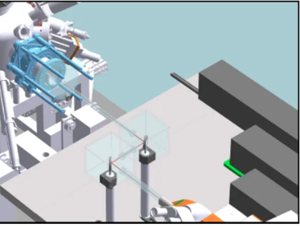
Figure 1.1: Laser path between the Raman spectrometer and the UHV system with an acrylic glass casing to decouple the laser path from the environment.
The spectrometer is a customized Renishaw inVia
T Msystem with four lasers of
different wavelength (332, 442, 532 and 633 nm). The collimated light from the
spectrometer is directly coupled onto the sample in the chamber and allows a
characterization without exposing samples to air. The laser path is separated
from the environment by an argon flooded acrylic glass casing (Figure 1.1)
with a laser beam focused on to the sample by a microscope objective in
a specially designed optical flange on the chamber. Two actuators on the
manipulator regulate the precise motion of the sample along two axes. This
allows the detection of small samples in combination with a camera and the
option to measure Raman maps with a spatial resolution of the Raman system
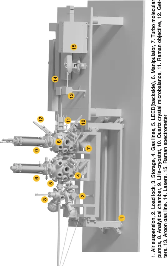
of 4 µm. The UHV system is supported by a frame on air loaded anti-shock
pads and provides a load lock for inserting samples, a storage, a preparation
chamber with different gas lines, evaporators and a LEED analyzer. This is
followed by an analytical chamber to measure the synthesized samples under
low temperatures without any exposure to ambient conditions. A liquid helium
cryostat allows permanent cooling to 4 K, a quartz crystal microbalance and
linear transfer devices for alkali metal getters and other substrate evaporators
for a functionalization of the measured materials round off the setup.
Figure 1.2: Complete measurement setup with the UHV system and Raman
spectrometer.
thick Au wires, glued by Ag paste to the spring pin connectors. The quantity
Figure 1.3: CAD drawing of the sample carrier with the correspond- ing sample receptor for electric transport measurements.
of the connectors was chosen by the motivation to measure 4-point resistance
with a further opportunity to gate the samples at the same time. The corre-
sponding sample receptor, permanently attached to the cryostat, was made of
CuBe to ensure a high thermal conductivity. Au covered nail pins, embedded
in a teflon block, act as a counterpart for the spring pin connectors on the sam-
ple plate. When the sample carrier is pushed into the receptor, the compressed
spring connectors present a reliable method for transport measurements even
under UHV conditions. Two screws additionally press the sample plate onto
the sample holder, to stabilize the latter and increase the thermal contact to
the cryostat. Au wires lead from the receptor to an electric feedthrough on top
of the cryostat and various multimeters in combination with a lock-in amplifier
complete the setup.
1.3 Electronic structure of graphene
Figure 1.4: a) Graphene lattice with carbon atoms A and B, nearest neighbor distance vectors δ
1−3, a
ccas the distance between two carbon atoms and the corresponding primitive lattice vectors a
1, a
2.
The electronic structure of an isolated carbon atom is given by:
(1s)
2(2s)
2(2p)
2The 2s and 2p electrons can hybridize and form a tetrahedral structure with four sp
3orbitals, formally known as diamond, which is a very good insulator (band gap ≈ 5 eV). An al- ternative possibility is to form three sp
2orbitals, leaving over a more or less pure p-orbital. Here the natural tendency for the sp
2orbitals is to arrange in a plane at 120
◦angles, giving a lattice in a honeycomb pattern shape named graphene. The structure of graphene is not a Bravais lattice but it can be seen as a triangular lattice with two atoms per unit cell. This lattice consists of two inequivalent sublat- tices A and B , shown in Figure 1.4, with the environments of the corresponding atoms being mirror images of one another. The corresponding primitive lattice vectors a
1, a
2can be written as:
a
1= a
cc2
3, √
3
, a
2= a
cc2
3, − √
3
(1.1) where a
ccis the nearest-neighbor carbon-carbon distance ( ≈ 1.42 Å). The re- ciprocal lattice vectors b
1, b
2defined by the condition a
i· b
j= 2πδ
ijare then
b
1= 2π 3a
cc1, √ 3
, b
2= 2π 3a
cc1, − √ 3
. (1.2)
The first Brillouin zone (BZ) of the reciprocal lattice is defined by the planes
bisecting the vectors to the nearest reciprocal lattice points. This gives the
first Brillouin zone (FBZ) of the same form as the original hexagons of the
honeycomb lattice, but rotated by π/2. The six points at the corners of the
momentum space are given by K = 2π
3a
cc1, 1
√ 3
, K
0= 2π 3a
cc1, − 1
√ 3
. (1.3)
For an A-sublattice atom the three nearest-neighbor vectors in real space are given by
δ
1= a
cc2
1, √ 3
, δ
1= a
cc2
1, − √ 3
, δ
3= − a
cc(1, 0) (1.4) while those for the B-sublattice are the negatives of these.
Tight-binding
The electronic band structure can be described with a tight-binding model that uses either ab-initio calculation parameters [Grneis2008] or is fit to experimental values [Grneis2009]. The graphene unit cell has two carbon atoms where each consists of one 1s, one 2s and three 2p orbitals, yielding to ten atomic orbitals all together. The 1s level is found 285 eV below the vacuum level and is not considered to contribute to the electronic properties.
Six of the remaining eight orbitals form the high energetic in-plane σ bonds turning into six bands. The residual two orbitals make the weak out-of-plane π bonds and therefore the π and π
∗bands, which will be considered in the electronic band structure in the following. Within the tight-binding approach, the eigenfunction Ψ
l(k, r) for a band with index l can be written as a linear combination of n Bloch wave functions Φ
m(k, r) [Bostwick2009]:
Ψ
l(k, r) = X
n m=1C
lm(k) · Φ
m(k, r) (1.5)
Φ
m(k, r) = 1
√ N X
NRa
e
ik·Ra· ϕ
m(r − R
a). (1.6) R
adenotes the atom position, ϕ
mis the atomic wave function in state m and the index N accounts for the N unit cells in the solid.
The coefficients C
lmof the eigenfunction Ψ
l(k, r) need to be determined by minimizing the eigenvalue E
l, which is a function of C
lm. This can be written as:
E
l(k) = h Ψ
l| H ˆ | Ψ
li
h Ψ
l| Ψ
li and ∂E
l∂C
lm∗= 0 (1.7) Inserting Ψ from (1.6) into (1.7) and minimizing the energy E
lleads to the expression for C
lm:
X
N m0H
mm0C
lm0(k) = E
l(k) X
Nm0
S
mm0C
lm0. (1.8) The integrals over the Bloch wave functions H
mm0and S
mm0are named transfer integral matrices and overlap integral matrices. By defining a column vector for C
lm0the matrix form of the eigenvalue equation can be written as:
H(k)C ˆ
l(k) = E
l(k) ˆ S(k)C
l(k). (1.9) The transposition of this equation leads to the secular form:
det
h H ˆ − E S ˆ i
= 0. (1.10)
If S ˆ is neglected for the nearest neighbor approximation which allows the hopping between the atoms A and B H ˆ = H
AAH
ABH
BAH
BB!
and H
ABgiven by H
AB= h Φ
A| H | Φ
Bi (1.11) leads to
H
AB= − t X
3i=1
e
ikδi(1.12)
with t as the hopping parameter. Therefore one can define:
f (k) = − t(e
−ik·δ1+ e
−ik·δ2+ e
−ik·δ3) (1.13)
q
where f(K) is zero. Therefore only the second term needs to be calculated:
∇ f (k) |
k=K= it δ
x1e
−ik·δ1+ δ
x2e
−ik·δ2+ δ
x3e
−ik·δ3·
q
x(1.16)
+ it δ
y1e
−ik·δ1+ δ
y2e
−ik·δ2+ δ
y3e
−ik·δ3· q
y(1.17)
= it a
cc2 e
(−i(2π/3)+ e
−i(0)− a
cce
i(−2π/3)· q
x(1.18) + it
√ 3a
cc2 e
−i(2π/3)− e
−i(0)!
· q
y(1.19)
= 3ta
cc4 ( √
3 + i)(q
x− iq
y). (1.20)
For K
0it follows:
∇ f (k) |
k−K0= 3ta
cc4 ( √
3 + i)(q
x+ iq
y) (1.21) To simplify the expression the pre-factor is written as p =
3ta4cc( √
3 + i) that gives the massless Dirac Hamiltonian
H ˆ
Graphene= 0 p(q
x+ τ iq
y) p
∗(q
x− τ iq
y) 0
!
(1.22) where τ = ± 1 indicates whether the Hamiltonian is centered on the K or K
0valley of the hexagonal Brillouin zone.
The eigenvalues E defined by Hv ˆ = λv are:
det( ˆ H − 1E) = E
2− pp
∗(q
2x+ q
y2) (1.23)
⇒ E = ± q
pp
∗(q
x2+ q
2y) (1.24)
= ± 3ta
cc2 q
q
2x+ q
2y(1.25)
− · the eigenvectors:
V
eigen1= 1
√ 2
p(qx−τ iqy)
√
pp∗(q2x+qy2)1
V
eigen2= 1
√ 2
−p(qx−τ iqy)
√
pp∗(q2x+qy2)1
.
(1.26)
Fermi velocity
Using the classical relation
dHdp= ˙ q with the momentum p and the velocity q, ˙ the correspondence of H → E, p → ~ k and q ˙ → v
Fleads to the Fermi velocity in graphene as [8]
v
F= 1
~ dE
dk = 1
~ 3ta
cc2 ( ≈ 1 × 10
6m
s ). (1.27)
Bandstructure
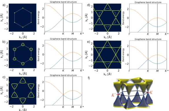
The theoretical electronic dispersion of pristine graphene along three high-
symmetry lines in the honeycomb lattice as shown in Figure 1.6(a) with the
energy in units of t. A tight-binding model with nearest neighbor approxima-
tion describes the evolution of the graphene Fermi surface under exposure to
Cs. Figure 1.6(b-e) shows the changes of the band structure starting from a
slightly doped (t = 0.1, 0.5)(a-b) to a heavily doped state just before(c), at(d)
and beyond(e) the Lifshitz transition [9, 10] (t = 0.9, 0.99, 1.01) and the Cs
induced filling of unoccupied states. The two convex Fermi surfaces turn into
one concave surface with a flat band at the M point of the Brillouin zone.
Figure 1.6: Evolution of the band structure and Fermi surfaces towards a Lifshitz transition in Cs doped graphene. a) pristine graphene, b-e) the evo- lution of the band structure with an increasing amount of Cs doping towards a Lifshitz transition, f) 3D view of e) adapted from [11].
Flat bands in graphene
A flat band in graphene can be induced by engineering the stacking order [12–
15], the twist angle (1.1
◦in bilayer graphene) [16, 17] and the doping level [18].
In the case of doping, the flat band at the M point of the Brillouin zone can be induced by sandwiching a graphene monolayer between two Cs layers. This is doping approach is a new technique to induce a flat band at E
Fof epitaxial graphene, caused by the combined effects of zone folding, hybridization and the excess of Cs/C stoichiometry. Zone folding of energy bands occurs in the periodic potential of alkali atoms, and was studied for graphite intercalation compounds [19] and alkali-metal doped bilayer graphene [20]. The zone folding refers to the folding of graphene bands into a smaller supercell, leading to an increased number of bands in the folded Brillouin zone. It causes the graphene bands close to E
Fto occupy a central region of the Brillouin zone.
Since the alkali metal band is also located around the Brillouin zone center
Cs band is possible. Without the zone folding, no hybridization would be possible, because the bands of graphene and Cs do not cross. A condition for the hybridization is that the alkali metal band is partially filled, i.e. the alkali atom should not be fully ionized. The conflicting conditions of a high doping that leads to a flat band and a partially occupied alkali metal band are combined by using highly ordered Cs layers on top of graphene and underneath graphene[Chapter 2.2].
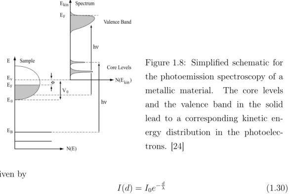
1.4 Photoemission spectroscopy
Photoemission spectroscopy measurements (PES) are based on the photo effect which was first observed by Hertz in 1887 [21] and later interpreted by Einstein in 1905 [22]. It allows the direct analysis of the electronic band structure and electron dispersion of solids.
E
kin= h · ν − Φ − E
B(1.28)
In Figure 1.8 the main principle of a light induced electron emission is shown.
Electrons with a binding energy E
Bare emitted from the valence band in the bulk surface when hit by photons with a specified energy h · ν which is big enough to overcome the work function Φ of the solid. Following equation (1.28) the exited electrons enter the vacuum with a kinetic energy E
kinand a certain momentum k which is related to the emission angle ϑ. The emitted electrons are detected by a hemispherical analyzer and a photoemission spectrum is observed. By applying a sufficient photon energy PES it is possible to analyze the density of states of the valence bands as well as the core level states. The photoemission process describes an excitation of an N -electron system with the energy E
iN= E
iN−1− E
Bkby a photon from a ground state to an excited state with E
fN= E
fN−1+ E
kinwhich should be ideally described in one step.
For the interpretation of photoemission experiments, the so-called three-step
model (Figure 1.8), describing the whole PES process in three separate steps,
has been proven to be extremely useful [24]. In this model, the one-step process
is divided into three independent and sequential steps that represent different
aspects of the problem:
(i) In the first step the photoionization takes place. A photon is absorbed locally and an electron is excited in the bulk of the solid.
(ii) The second step describes the transport of the excited electron inside the bulk to the surface.
(iii) The third step describes the escape of the photoelectron through the surface potential barrier into the vacuum, where it is detected.
The photoexcitation probability per unit time is described by Fermi’s golden rule:
ω
f i= 2π
~ | h Ψ
Nf| H
int| Ψ
Nii|
2δ(E
fN− E
iN− hν). (1.29) The excitation process can be described as a transition of the electronic sys- tem from an initial to a final state. In the initial state, the electronic system of the solid is described by an N -electron wave function Ψ
i. After photoex- citation, the system is described by another N -electron wave function Ψ
f, comprising the N -1 electrons remaining in the solid plus the emitted pho- toelectron. During the transport through the solid, the electrons undergo elastic and inelastic scattering owing to the potential of the crystalline solid.
The elastically scattered outgoing photoelectron waves are diffracted in the solid. This effect can be applied as a method to determine the geometrical environment of an emitting atom. Due to inelastic scattering, photoelectrons lose kinetic energy by exciting secondary electrons, plasmons, and phonons.
This limits the escape depth of the photoelectrons, described by λ, the so-
called inelastic-mean-free path. The intensity I(d) of the emitted electrons is
Figure 1.8: Simplified schematic for the photoemission spectroscopy of a metallic material. The core levels and the valence band in the solid lead to a corresponding kinetic en- ergy distribution in the photoelec- trons. [24]
given by
I(d) = I
0e
−λd(1.30) where I
0is proportional to the number of the excited electrons.
During the escape of electrons into the vacuum only the parallel component of the wave vector is conserved modulo a reciprocal surface wave vector due to the periodicity of the lattice potential parallel to the surface. Neglect- ing "umklapp"-processes k
kcan be described with the kinetic energy and the emission angle ϑ by
k = k
⊥+ k
k= p/ ~
| k | = √
2 · m · E
kin/ ~
k
k=
1~
√ 2 · m · E
kin· sin(ϑ)
(1.31)
Measuring E
kinand ϑ in PES experiments fixes k
kwhich is sufficient for sur- face states but not for bulk bands. To measure the band dispersion along a direction perpendicular to surface a variable photon energy source is necessary.
Due to the discontinuity of the potential at the surface/vacuum interface, the perpendicular component of the electron wave vector is not conserved. The component normal to the surface is given by
k
⊥= 1
~
p 2 · m · (E
kin· cos
2(ϑ) + V
0) (1.32)
by ∆E
a= E
pass(ω/R
0+ α
2/4); where R
0= (R
1+ R
2)/2; ω is the width of the entrance slit, and α is the acceptance angle. Either synchrotron light or gas discharge lamps can be used as a light source. The disadvantage of gas discharge lamps is the limited photon energy of 21.2 eV or 40.8 eV but the costs are much lower compared to synchrotron light which is tunable regarding pho- ton energy and features a much higher brilliance. The measurements in these thesis were taken at Elettra Synchrotron Triest (Figure 1.9) in Italy at the beamline BaDElPh.
Figure 1.9: Elettra light source [25].
1.5 Raman spectroscopy
Scattered light can be thought of as a redirection of light that takes place
when an electromagnetic wave encounters an obstacle. When the electromag-
netic wave interacts with matter, the electron orbits within the constituent
molecules are perturbed periodically with the same frequency as the electric
field of the incident wave. The oscillation of the electron cloud results in
duced dipole moment. The oscillating induced dipole moment manifests as an electromagnetic radiation source and therefore results in scattered light.
The majority of the scattered light is emitted at the identical frequency of the
Figure 1.10: Schematic for Rayleigh and Ra- man
(Stokes and anti-Stokes) scattering.
incident light. This process is due to elastic scattering. Ad- ditional light is scattered at different frequencies, which is referred to inelastic scattering and Raman scattering is one such example of inelastic scat- tering. When the incident electromagnetic wave induces a dipole moment during the light-material interaction, the strength of the induced dipole moment, P, is given by [26]
P = α · E ¯ (1.33)
with α as the polarizability and E ¯ is the strength of electric field of the in- cident electromagnetic wave. The polarizability is a material property and depends on the molecular structure and nature of the bonds. For the incident electromagnetic wave, the electric field can be expressed as
E ¯ = E
0cos(2πν
0t) (1.34) where ν
0is the frequency of the incident wave (ν
0= c/λ). Substituting Eq.
(1.34) into (1.33) gives the time-dependent induced dipole moment,
P = α E
0cos(2πν
0t). (1.35)
For any molecular bond, the individual atoms are confined to specific vibra-
tional (rotational) modes. The vibrational energy levels are quantized in a
manner similar to electronic energies. The vibrational energy of a particular
mode is given by E
vib= (j + 1/2) h ν
vibwith j as the vibrational quantum
number (j = 0,1,2...), ν
vibas the frequency of the vibrational mode, and h is
the Planck constant. The physical displacement dQ of the atoms about their
Based on the vibrational displacement of Eq.(1.36), the polarizability is given by
α = α
0+ ∂α
∂Q Q
0cos(2πν
vibt). (1.38) Finally, Eq.(1.38) may be substituted into Eq.(1.35), which yields
P = α
0E
0cos(2πν
0t) + ∂α
∂Q Q
0E
0cos(2πν
0t) cos(2πν
vibt). (1.39) With use of a trigonometric identity, the relation can be recast as
P = α
0E
0cos(2πν
0t)+ ∂α
∂Q Q
0E
02 cos
2π (ν
0− ν
vib)t +cos
2π (ν
0− ν
vib)t . (1.40) The induced dipole moments are created at three distinct frequencies, ν
0, (ν
0− ν
vib), and (ν
0+ ν
vib), resulting in scattered radiation at these three fre- quencies. The first scattered frequency relates to the incident frequency and is elastic scattering (Mie or Rayleigh) as depicted in Figure 1.10. The other frequencies are shifted to lower or higher wavenumbers and are hence inelastic processes. The scattered light in the latter two cases is the Raman scatter- ing with the down-shifted frequency as Stokes scattering, and the up-shifted frequency as anti-Stokes scattering. The necessary condition for Raman scat- tering is that
∂Q∂αmust be non-zero meaning that the vibrational displacement of atoms corresponds to a particular vibrational mode that result in a change in the polarizability.
To perform Raman spectroscopy a laser as the excitation source is generally
used. The intense, collimated monochromatic light allows measurements of
relatively small Raman shifts, while the intense beam improves the spatial
resolution and signal-to-noise ratio. Usually, the Raman signal intensity is
scattering. Therefore spectrometers are used with notch filters or edge filters (sharp cut-off high pass filters) to separate the elastic scattering and Raman scattering signals and reject the elastically scattered light prior to entering the spectrometer.
Raman spectroscopy in graphene
A typical Raman spectrum of graphene is dominated by two bands, one at
≈ 1580 cm
−1and another at ≈ 2700 cm
−1. The former is the G band, the only allowed first order Raman band. The second band is the result of a higher order process involving two phonons. This band has been referred to as 2D mode|
and originates from a double resonance process. The G mode originates from the E
2gin-plane phonon at the Γ point where the longitudinal optical (LO) and transverse optical (TO) branches touch each other whilst the 2D is a result of a double resonance enhanced two-phonon process and only zone-boundary phonons have proper frequencies for this. In fact, the 2D band originates from two TO phonons around the K point. Another band at ≈ 1350 cm
−1and is called the D band which is a disorder induced band. The intensity of this band increases with increasing levels of disorder. This band is at half the frequency of the 2D band: the 2D is the overtone of the D band, which is noteworthy because the 2D band does not require any disorder. It is worth to note that there is also another band induced by disorder at ≈ 1620 cm
−1called D
0band. This band is very similar to the D band except that the phonons generating it are in the vicinity of the Γ point, not the K point [27, 28].
Electronic Raman scattering
In graphene, the shape and position of the Raman spectra can give a deep
understanding of the electron energy dispersion [29], phonon energy dispersion
[30], the Kohn anomaly [5], and structure characterization [31]. Especially
the asymmetric Breit-Wigner-Fano (BWF) line shape, observed in the Ra-
man spectra of graphite intercalation compounds [32] and metallic nanotubes
[33], probes the interference between the continuum spectra with the discrete
spectra [4]. The origin of the Fano line shape in graphene comes from the con-
Raman intensity of the spectra, respectively. When 1/q = 0 the equation (1.41) gives a Lorentzian line shape which represents a discrete phonon spectrum indicating no interference effect.
1.6 Transport properties of graphene
Figure 1.11: UHV transport setup
Transport measurements were taken under UHV conditions using a spe- cial sample carrier with the corre- sponding sample receptor, as shown in Figure 1.3. The measurement ge- ometry is depicted in Figure 1.11 with the sample glued on a quartz or Al
2O
3plate, insulating the sample from the molybdenum carrier. The setup features five contacts allow- ing the simultaneous measurement of resistance in a four-point geometry in combination with additional back- gating. For a geometry of an infinite graphene sheet with contacts within the graphene, the resistance is deter- mined by:
R = 2π ln(2) · V
I (1.42)
on a square [35]. The sheet resistance given by the van der Pauw technique requires several conditions that must be satisfied:
1. The sample must be flat and have a uniform thickness.
2. The sample must have no isolated holes.
3. The sample must be isotropic and homogeneous.
4. All contacts must be located at the edge of the sample.
In addition to these conditions, the area of any of the contacts must be at least an order of magnitude smaller than the area of the entire sample. In the case of a ratio of contact to sample perimeter less than approximately 0.3, there is negligible correction to the ideal van der Pauw formula [36]. For this the four-point resistance is given by:
R = π ln(2) · V
I (1.43)
The calculation of doping induced charge carriers is analyzed by the shift of the resistance curve versus gate voltage. The charge carrier density n is estimated according to:
n = CV
eA (1.44)
with C =
0· A/d (here C is the sheet capacitance of the back gate, V
Dthe gate voltage of maximum sheet resistance, e is the elementary charge,
(0)the vacuum permittivity respectively for SiO
2, and d the thickness of the oxide layer). For a 300 nm SiO
2wafer we get C = 11.5
cmnF2with = 3.9 [37].
The quality of the transferred graphene can be estimated from the field effect mobility µ
F Ewhich is given as:
µ
F E= 1
C · d(
R1)
dV . (1.45)
Here
d(1 R)
dV
is the derivative of the reciprocal sheet resistance with respect to
the gate voltage V.
2.1 Resonance Raman spectrum of doped epi-
taxial graphene at the Lifshitz transition
Resonance Raman Spectrum of Doped Epitaxial Graphene at the Lifshitz Transition
Martin G. Hell,
†Niels Ehlen,
†Boris V. Senkovskiy,
†Eddwi H. Hasdeo,
‡,§Alexander Fedorov,
†Daniela Dombrowski,
†,⊥Carsten Busse,
†,¶Thomas Michely,
†Giovanni di Santo,
∥Luca Petaccia,
∥Riichiro Saito,
‡and Alexander Grüneis*
,††II. Physikalisches Institut, Universität zu Köln, Zülpicher Strasse 77, 50937 Köln, Germany
‡Department of Physics, Tohoku University, Sendai 980-8578, Japan
§Research Center for Physics, Indonesian Institute of Sciences, Kawasan Puspiptek Serpong, Tangerang Selatan 15314, Indonesia
⊥Institut für Materialphysik, Westfälische Wilhelms-Universität Münster, Wilhelm-Klemm-Str. 10, 48149 Münster, Germany
¶Fakultät IV Physik, Universität Siegen, Walter-Flex-Str. 3, 57072 Siegen, Germany
∥Elettra Sincrotrone Trieste, Strada Statale 14 km 163.5, 34149 Trieste, Italy
*
S Supporting InformationABSTRACT: We employ ultra-high vacuum (UHV) Raman spectroscopy in tandem with angle-resolved photoemission (ARPES) to investigate the doping-dependent Raman spectrum of epitaxial graphene on Ir(111). The evolution of Raman spectra from pristine to heavily Cs doped graphene up to a carrier concentration of 4.4×1014cm−2is investigated. At this doping, graphene is at the onset of the Lifshitz transition and renormalization effects reduce the electronic bandwidth. The optical transition at the saddle point in the Brillouin zone then becomes experimentally accessible by ultraviolet (UV) light excitation, which achieves resonance Raman conditions in close vicinity to the van Hove singularity in the joint density of states.
The position of the RamanGband of fully doped graphene/Ir(111) shifts down by∼60 cm−1. TheGband asymmetry of Cs doped epitaxial graphene assumes an unusual strong Fano asymmetry opposite to that of theGband of doped graphene on insulators. Our calculations can fully explain these observations by substrate dependent quantum interference effects in the scattering pathways for vibrational and electronic Raman scattering.
KEYWORDS: Alkali doping, graphene, UHV Raman, ARPES, Lifshitz
R
aman spectroscopy is the most widely used character- ization method for graphene.1−4 The electron and phonon systems of graphene are strongly coupled to each other by electron−phonon interactions.5,6These interactions manifest as “kink” features in the electronic spectral function7−12and as Kohn anomalies in the phonon dispersion relations around the Brillouin zone (BZ) center (Γpoint) and corners (K points).5,6 As a consequence, the carrier concentration of graphene sensitively affects the position, line shape, and intensity of thefirst- and second-order Raman spectra corresponding to these phonon modes. The effects of phonon renormalization due to the removal of the Kohnanomaly or lattice expansion on the phonon energy are quantitatively understood.5Phonon renormalization results in a phonon upshift for Fermi level positions higher than half the phonon frequency (measured from the Dirac point) and lattice expansion results in a phonon downshift.5,6Experimentally, phonon hardening has been observed in Raman measurements where the charge carrier concentration of graphene has been tuned byfield effect gating6,13or by ionic liquid gating.14−16 Received: July 21, 2018
Revised: August 21, 2018 Published: August 29, 2018
Letter pubs.acs.org/NanoLett Cite This:Nano Lett.2018, 18, 6045−6056
© 2018 American Chemical Society 6045 DOI:10.1021/acs.nanolett.8b02979
Nano Lett.2018, 18, 6045−6056
The latter approach has been used to induce large carrier densities of 6×1013cm−2(ref15). Even for such high carrier concentrations, phonon hardening due to phonon self-energy corrections dominates.5However, when the carrier density is in the 1014 cm−2 range that has already been probed by transport,17,18the Fermi energy can be in the vicinity of the van Hove singularity at theMpoint in the Brillouin zone and phonon softening will then dominate. Achieving and probing high carrier densities is fundamentally important for both conventional19−21and chiral superconductivity22in monolayer graphene. The latter case requires the Fermi level to touch the saddle point van Hove singularity at theMpoint in the two- dimensional (2D) BZ. In this case, the Fermi surface of graphene assumes a closed shape centered at theΓpoint rather than two surfaces centered around theKandK′points. The transition of topology from two Fermi surfaces to one Fermi surface marks the Lifshitz transition23in graphene.
The present work aims at understanding the peculiar Raman spectrum of graphene at the Lifshitz transition and unravelling the deep underlying connection between electronic band
structure and phonon renormalization in heavily doped graphene. To that end, we synthesize Cs doped graphene up to the highest achievable carrier concentrations. The energy bands are renormalized significantly due to doping and are probed by angle-resolved photoemission spectroscopy (ARPES) for each doping step. Despite the fact that Raman spectroscopy is typically not considered a surface science method, we present an original ultrahigh-vacuum (UHV) Raman setup that employs a commercial Raman system coupled to a UHV system. From these experiments, we can relate the observed changes in the vibrational and electronic spectrum to band structure changes. We thus obtain a complete picture of the coupled electron−phonon system in epitaxial graphene.
McChesney et al. already experimentally observed the Lifshitz transition in heavily doped graphene using ARPES.24 Their keyfinding was that the band structure of heavily doped graphene is strongly renormalized, yielding aflat conduction band at the Fermi level, that is, an extended van Hove singularity.24Importantly, the renormalization also reduces the Figure 1.(a) ARPES scans of Cs doped graphene/Ir(111) in theΓKMdirection (top panel) and Fermi surface maps (bottom panel) for different Cs coverages. The shift of the Dirac point is indicated in the top panel and the carrier concentration of graphene per cm2is indicated in the bottom panel. (b) High-resolution ARPES data in the vicinity of the kink feature along theΓKdirection. Black and green lines denote ARPES intensity maxima and the bare band, respectively. (c) Real and imaginary part of the self-energy (denoted asℜeΣandℑmΣ) for different doping levels. (d) Eliashberg functions (blue) and contribution of theGband phonon (orange) alongΓKas a function of carrier concentration. The orange lines in panel c denote the self-energy functions that are calculated from these Eliashberg functions. (e) Fit of the deformation potentialD2(see text for details). (f) Tight-binding calculation of the Fermi surfaces of doped graphene (blue regions) for carrier concentrations just before and beyond the Lifshitz transition.
transition energy at the saddle point between valence and conduction bands. Indeed, Mak et al. found that the energy of theMpoint transition is reduced by ∼200 meV when going from charge neutrality to 1×10¹⁴carriers per cm2(ref25).
For graphene, thefirst-order Raman spectrum due to zone- center optical phonons with in-plane polarization (theGband) shows an asymmetric Fano line shape if graphene is doped by field effect gating26or alkali metal doping.27This line shape is reproduced theoretically by considering the interference between a discrete transition (phonon) to a continuum (excitation of electron−hole pairs), which is known as electronic Raman spectra (ERS).28−31 The Fano line shape of theGband is more pronounced for larger doping levels26 and for a higher layer number.27The most pronounced Fano asymmetries are obtained in stage 1 graphite intercalation compounds such as KC8.32,33 Doping also has a strong influence on theGband intensity,34which is determined by quantum interference in the Raman scattering pathways.15,35 Upon doping, transitions between two occupied (unoccupied) states are forbidden by Pauli blocking and do not contribute to the total Raman intensity. As a consequence, the G band intensity as a function of doping level is peaked for the condition 2EF = Elaser− Eph/2. Here EFis the Fermi level position measured from the charge neutrality point,Elaserthe excitation energy, andEphtheGband phonon energy.15
Apart from the limits regarding carrier concentration, ionic liquid gating experiments also block the direct access to the sample surface. This precludes direct observation of the electron energy band structure of gated graphene by ARPES. It thus prohibits a detailed understanding of the nonrigid band shifting and electron−phonon coupling in heavily doped graphene that has been achieved for chemically doped graphene.7−12,24An approach to carry out Raman spectroscopy of chemically doped graphene is to measure it inside a quartz ampule. For example, alkali metal doped graphene27,36,37and FeCl3 doped graphene38 have been measured in this way.
Unfortunately, such experimental setups also preclude band structure measurements by ARPES, structural characterization by low energy electron diffraction (LEED), and efficient sample cooling to liquid He temperatures. Moreover, in the case of alkali doping inside quartz ampules, a fraction of the dopant atoms will be oxidized because of poor vacuum conditions. Combined ARPES and Raman experiments in UHV conditions would not suffer from these drawbacks.
Previously, the investigation of the electronic structure of doped graphene has been performed using the standard surface science methods such as ARPES9,39,40and scanning tunneling spectroscopy (STS).21,41These probe the electronic structure of epitaxially grown graphene and directly reveal Fermi level shifts, spectral functions, and superconducting gaps as a function of dopant concentration and type and substrate interactions. Much less is known about the phonons and low energy electronic excitations in alkali metal doped epitaxial graphene despite these contain valuable information regarding doping level, strain, and electron−phonon coupling.
Experimental Results.Electronic Structure of Cs Doped Graphene/Ir(111).InFigure 1a, we show ARPES spectra of pristine and Cs doped graphene. For each amount of deposited Cs, we also have performed structural characterization by LEED (see Supporting Information). Pristine graphene on Ir(111) (seeMethodssection for details pertaining synthesis) has the R0 structural phase.42This is confirmed by the moiré
pattern observed in LEED. The moirépattern is a result of
corrugations due to chemically modulated substrate inter- action.43 It hosts weakly covalently bonded regions with a small charge transfer from graphene to Ir(111).43 Using ARPES (Figure 1a), we find in agreement to previous literature42,44 that R0 graphene/Ir(111) is only weakly hole doped. After depositing Cs onto the sample surface at room temperature, wefind that the moirépattern observed in LEED disappears and only thefirst order diffraction spots are left.
This LEED pattern is denoted as 1×1 in the following. The disappearance of the moirépattern upon Cs deposition is an indication of a change in the graphene−substrate interaction.
The graphene−Ir(111) interaction also manifests in mini- gaps,44which are visible in the ARPES spectrum as regions of weakerπ band intensity. After Cs deposition, these minigaps disappear, indicating that Cs doping weakens the local variations in the graphene−Ir(111) interaction. We expect that the charge transfer to graphene becomes homogeneous and removes the hybridization of C and Ir bands. ARPES also confirms a single doping phase as only one Dirac cone is visible. Increasing the Cs amount, we are able to reach an ordered 2 × 2 phase of Cs on graphene as reported previously.45 This phase also has a single Dirac cone in ARPES. Analysis of the experimental Fermi surface from ARPES measurements yields a carrier concentration ofn= 1.5
× 1014 cm−2. Further increasing Cs deposition leads to the
×
3 3 phase in LEED and a slightly higher doping level.
Here we haven= 1.5×1014 cm−2. To confirm the ARPES derived carrier densities by another method, we also performed Fourier transform scanning tunneling spectroscopy (FT-STS) measurements41(seeSupporting Information). These indicate carrier concentrations of 1.7×1014cm−2for the 2×2 phase and 1.9× 1014 cm−2 for the 3 × 3 phase. The carrier concentration for the 2×2 is in excellent agreement to the value from ARPES and to previous experiments.45However, the concentration for the 3 × 3 phase from FT-STS is lower by a factor∼1.3 when compared to ARPES. This can be understood by the 3 × 3phase corresponding to graphene fully intercalated with Cs. Any extra Cs lies on top of graphene and a system with small amounts of extra Cs on top still shows a 3 × 3diffraction pattern in LEED. Thus, the 3 × 3 phase exists for a broader range of adsorbate concentrations and can slightly vary from system to system. Thus, LEED is a good measure of stoichiometry for the 2×2 phase only. To ensure depositing of equal Cs amounts in the Raman and ARPES investigations, we calibrated the deposited Cs using a quartz microbalance as a multiple of the amount of Cs needed for reaching the 2×2 phase. Since the 2×2 phase is well- defined, this approach yields reproducible sample stoichiome- tries for different samples and in different experimental setups.
Evaporation of excess Cs onto the sample does not result in an ordered phase according to LEED but it is still possible to increase the graphene doping level. Atn= 3.1×1014cm−2(see Figure 1a), we already see marked deviations from the usually observed trigonal warping in ARPES. As is shown inFigure 1a (bottom row), the warping direction changes from convex to concave. We are able to reach a value ofn= 4.4×1014cm−2 (for the highest value of n, see Supporting Information).
Regarding the relation between Cs/C stoichiometry and carrier concentration, we note that each Cs atom may donate less than one electron. However, this does not affect the carrier densities determined from ARPES because this method is not dependent on the stoichiometry but directly measures the
Nano Letters Letter
DOI:10.1021/acs.nanolett.8b02979 Nano Lett.2018, 18, 6045−6056 6047
carrier concentration of graphene from the area of the Fermi surface of graphene.
Let us now turn to the analysis of electron−phonon coupling. Figure 1b depicts high resolution scans of the
“kink” feature at low binding energy. We first perform a standard self-consistent self-energy analysis7−9of ARPES data in the kink region yielding the complex self-energy and the Eliashberg function. These are depicted in Figure 1c and d, respectively. By integrating the Eliashberg function of graphene8 in the region of the G band, we obtain λG, the electron−phonon coupling constant for the G mode that is frequently used in ARPES literature. The Raman community often expresses electron−phonon coupling by the deformation potential D2. The deformation potential and the electron−
phonon coupling constantλGare connected asλG=N(0)D2/ (Mω2) (see ref19). HereN(0) is the electron density of states per unit cell, per eV, and per spin at the Fermi level,Mthe carbon mass, andωtheGband frequency. The resultingfit of four charge carrier concentrations is depicted inFigure 1e and yields D2 = 61.3 eV2/Å2. Finally, Figure 1f depicts a tight- binding calculation of the Fermi surfaces at carrier concen- trations just before and beyond the Lifshitz transition. In this figure, we show Fermi surface contours atn= 3.7×1014cm−2 and atn= 5.6×1014cm−2. For the higher concentration ofn= 5.6×1014cm−2, we are already above the Lifshitz transition (i.e., the Fermi surface is a single contour) while the lower concentration is just before the Lifshitz transition (i.e., the Fermi surface consists of two contours that almost touch). For the calculation of these Fermi surface contours, we have employed a third-nearest-neighbor tight-binding model46 where the matrix elements are fitted to the experimental ARPES band structure. It is clear that the carrier concentration at which the Lifshitz transition happens is in between these two concentrations. Using the same tight-binding model, we estimate a value of n =4.4 ×1014cm−2 where the Lifshitz transition is observable. We expect that the Lifshitz transition is induced purely by doping because we do not observe a lattice deformation. This is corroborated by the diffraction pattern of an overdoped sample above the 3 × 3phase to a doping level close to the Lifshitz transition. The diffraction pattern of this sample [shown in theSupporting Information in
Figure S2(e)] still shows sharp spots in a hexagonal pattern that are due to graphene.
Raman Spectrum of Epitaxial Graphene/Ir(111).InFigure 2, we show the Raman spectra atT= 300 K and atT= 5 K of epitaxial graphene/Ir(111) measured by lasers with wave- lengths 633 mm, 532 nm, 442 nm, and 325 nm. The depicted spectra are the average over 25 points chosen along a scan across 120μm on the surface. In principle, for interpretation of the observed temperature-dependent spectra, in-plane strain and wrinkle formation due to the different thermal expansion coefficient of graphene and the Ir substrate must be considered.47−49 Only the ultraviolet (UV) laser (325 nm) results in a strong Raman signal at room temperature. Upon cooling, the spectra taken by 532 and 442 nm excitation show a weak Raman signal, which could be a sign of temperature induced changes in the substrate interaction. These observa- tions extend previous works reporting the absence of a Raman signal for graphene/Ir(111) that belongs to theR0 structural phase for visible excitation at room temperature.42So far, no quantitative explanation regarding the absence of a Raman signal for visible laser excitation forR0 graphene on Ir(111) has been given. We speculate that it could be explained in terms of minigaps,44which appear at certain energies in the band structure. It has been shown by ARPES that the minigaps are in all directions aroundKpoint and close nowhere.50If the laser energy hits a minigap, no electrons can be excited between the valence and conductionπbands of graphene and the Raman intensity is suppressed. The high quality of graphene is also corroborated by the absence of a defect related D peak. Interestingly the 2D peak is absent in all measurements. This observation is in agreement to previous works and might be related to the short lifetime of photoexcited charge carriers in graphene adsorbed on metals, which suppress the 2D intensity.51
Temperature Induced Strain in Epitaxial Graphene.Let us now move to the Raman analysis of strain52,53induced by the temperature-dependent change in the lattice constant. For epitaxial graphene on Ir, the thermal expansion of graphene essentially follows the substrate.54The nonlinearity inTof the thermal expansion coefficientα(T) of iridium must be taken into account.55,56To accurately describe the expansion of the Ir substrate in the temperature range explored (5 K−300 K), Figure 2.(a) Ultra-high vacuum (UHV) Raman spectrum of pristine graphene/Ir(111) atT= 5 K andT= 300 K for four different laser wavelengths in the range between red and ultraviolet. The dashed lines denote the experimental data and solid lines Lorentzianfits. TheGband taken at 325 nm excitation shows an upshift in frequency upon cooling (indicated by arrows in the lower panel). The sharp line at 1555 cm−1is due to oxygen in the unavoidable part of the laser path outside the vacuum (seeSupporting Information Figure S1for a sketch of the UHV Raman setup). (b) Linescan of the Raman spectrum (at 325 nm) across a 120μm distance of the sample.
wefitα(T) to literature values55,56and calculate the expansion asl′/l= exp (∫α(T) dT). Herel′andlare the lattice constants at temperatures corresponding to the upper and lower border of the integral, respectively. For describing the Ir lattice expansion of the present experiment, the integral above is taken fromT= 5 K toT= 300 K. The strainεin percent is calculated as 100(l′/l−1) yieldingϵ= 0.134%. The phonon downshift corresponding toϵis given byΔω=−2ω0γϵ(see ref 57 and references therein). Here γ = 1.99 (ref 57) is the Grüneisen parameter of the doubly degenerate G phonon mode of graphene,ω0= 1606.5 cm−1is the phonon frequency at 5 K. These values yield a strain induced downshift of the G band phonon when going from 5 to 300 K ofΔω =−8.6 cm−1, which is in excellent agreement to the experimental value ofΔω=−10.7 cm−1.
Raman Spectrum of Cs Doped Graphene/Ir(111).We have used a Fano line shape30,36,58,59
to fit the G band Raman spectra for all doping levels by
ω = +
+
ω ω γ ω ω
γ
−
−
( )
( )
F( ) I 1 1
q 0
/ 2 2
/ 2 2 0
0
(1) HereI0is the Raman intensity,ω0the line position,γthe full- width at half-maximum, and 1/q the asymmetry (or Fano) factor, which describes the strength of the interference effect between the discrete and continuous spectra. For 1/q= 0, we have a Lorentzian line shape indicating no interference effect.
In the following, we analyze the carrier concentration dependence of I0,ω0,γ, and 1/q. Figure 3a illustrates that, upon evaporation of Cs onto the sample, the observed Raman spectra dramatically change compared to those of pristine graphene. For the first deposition of Cs, all laser energies except the red laser (633 nm) yield afinite Raman intensity.
We attribute the appearance of a Raman signal to removal of the hybridization of the graphene and Ir states as discussed in
the ARPES section. From Figure 3a, we observe that the Raman intensity almost vanishes for the green (532 nm) laser at a carrier concentration of 2.4×1014cm−2(corresponding to the 3 × 3 phase). The Raman intensity for the blue laser (442 nm) vanishes at a doping level of 3.1×1014cm−2. On the other hand, the UV laser (325 nm) yields a Raman spectrum up to the highest doping level. This can be understood in terms of the condition that light can only induce transitions across the Dirac cone between occupied states in the valence band and unoccupied states in the conduction band. If doping shifts the Fermi level deep into the conduction band, these transitions are forbidden by Pauli blocking. The UV laser always fulfills the resonance condition 2EF<Elasersince its laser energy (Elaser= 3.8 eV) is significantly higher than twice the maximum Fermi level shift (EF= 1.58 eV from the ARPES data of maximally doped graphene).
Figure 3a also reveals that the Raman spectrum taken with the lowest photon energy for each doping level becomes Fano- like. This applies to the 532 nm (green) laser for 1.5×1014 cm−2, the 442 nm (blue) laser for 2.4×1014cm−2, and the UV laser for 3.1×1014cm−2. The most striking feature is that the Fano tail of the present data is toward higher wavenumber with respect to the peak position. This corresponds to a positive sign of 1/q. The origin of this unusual Fano line shape will be explained in the next section. In Figure 3b, we show UV Raman spectra with increasing carrier concentration. The position of theGpeak shifts toward higher phonon energies for carrier concentrations up to 1.5×1014cm−2before it shifts down. The UV Raman spectrum allows for comparison of the G line position of pristine (1606.3 cm−1), weakly doped graphene (1615.9 cm−1for the lowest Cs deposition), and fully doped graphene (1550.0 cm−1). A key to understanding the present results is the interference of the electronic and vibrational Raman, which also plays a major role in explaining the Fano asymmetry in carbon nanotubes.28Here we apply this theory30 using the experimental band structure of graphene derived from ARPES measurements. The calculated Raman Figure 3.(a) Ultra-high vacuum (UHV) Raman spectra of Cs doped epitaxial graphene/Ir(111) with increasing carrier concentration from left to right measured by four laser lines. The raw data (dots) of the RamanGband together with a Fano line shapefit are shown. (b) UHV ultraviolet Raman spectra of doped graphene with increasing carrier concentration measured with 325 nm excitation. All Raman spectra are taken atT= 5 K and a vacuum better than 2×10⁻¹⁰mbar. (c) Calculated Raman spectra for 325 nm light excitation and identical carrier concentrations as in panel b.
Nano Letters Letter
DOI:10.1021/acs.nanolett.8b02979 Nano Lett.2018, 18, 6045−6056 6049
spectra are depicted inFigure 3c and a very good agreement regarding the position and Fano asymmetry can be seen. In the following section, we will show a quantitative comparison between experiment and theory regarding the position and asymmetry of theGband and discuss the details of the Raman calculation. Let us now look to the temperature dependent Raman spectra of doped graphene. This is motivated by question if intercalation of Cs liberates graphene from the substrate so that it does not follow any more the lattice constant of Ir. The corresponding Raman spectra and theG band positions are shown inFigure 4. An upshift of theGband position by 7 cm−1with decreasing temperature (from 300 to 5 K) is found. This is within the experimental accuracy to what we observed inFigure 2for pristine graphene/Ir. Thus, despite Cs is intercalated in between graphene and Ir(111), the graphene still follows the compression of the underlying Ir substrate.
Discussion. Electronic Raman Scattering. In the elec- tronic Raman scattering, the photoexcited electron and hole couple to electronic excitations via the Coulomb interaction and can generate one or more electron−hole pairs. The large density of states in heavily doped graphene around theMpoint
enhances the cross-section for electronic Raman scattering. In Figure 5a and b, we graphically depict the relaxation processes, which we consider in the calculation. We considerfirst-order (creation of one electron−hole pair) and second-order (creation of two electron−hole pairs) processes. The Coulomb interaction is affected by the dielectric screening of the substrate, which is strong for the Ir substrate (ε= 50).60As a consequence, only thefirst-order process (wavevectorq= 0) is dominant for Ir. This is depicted inFigure 5c. We note that thisfirst-order process excites an intraband electron−hole pair whose Coulomb interaction is maximum at wavevectorq= 0.
This process is completely different from the interband electron−hole pair excitation in the low doping regime, in which the direct Coulomb interaction vanishes atq= 0.31
Interference between the first-order ERS (shown by the green line) and the G band (red line) produces the asymmetric Fano line shape toward larger wavenumber (1/q> 0).Figure 5d depicts the simulated Raman spectra of highly doped graphene on SiO2 substrate. Because of the relatively weak screening effect (ε = 4), the second-order Raman (q≠ 0) process overcomes thefirst-order process thanks to the double resonant effect. The resulting Raman spectra are asymmetric Figure 4.(a) Temperature dependent Raman spectra of the 3× 3phase of Cs doped graphene for cooling (blue line) and warming-up (red line). (b) Raman peak positions as a function of temperature.
Figure 5.(a) In thefirst-order electronic Raman scattering (ERS) process, an electron is excited to a virtual state above the saddle-point energy and then relaxes via Coulomb interaction by exciting an e−h pair. When the electron recombines with the hole, the scattered energy is resonant to the Mpoint energy. (b) In the second-order ERS process, the photoexcited e−h pair occupies a real state. The electron and hole relax to lower energy states by exciting two e−h pairs near Fermi surface with oppposite momenta. Calculated Raman spectra of highly doped-graphene on (c) Ir substrate and (d) SiO2substrates. The dashed lines indicate the spectral contributions of the vibrational Raman scattering by theGphonon and ERS. The solid line is the spectrum after considering interference between these two contributions.


![Figure 1.9: Elettra light source [25].](https://thumb-eu.123doks.com/thumbv2/1library_info/3698385.1505905/20.892.259.679.621.813/figure-elettra-light-source.webp)


