Resonance Raman spectrum of doped epitaxial graphene at the Lifshitz transition
Martin G. Hell, † Niels Ehlen, † Boris V. Senkovskiy, † Eddwi H. Hasdeo, ‡ Alexander Fedorov, † Daniela Dombrowski, † Carsten Busse, † Thomas Michely, † Giovanni di Santo, ⊥ Luca Petaccia, ⊥ Riichiro Saito, ‡ and Alexander Gr¨ uneis ∗,#
II. Physikalisches Institut, Universit¨ at zu K¨ oln, Z¨ ulpicher Strasse 77, 50937 K¨ oln, Germany, Department of Physics, Tohoku University, Sendai 980-8578, Japan, Research
Center for Physics, Indonesian Institute of Sciences, Kawasan Puspiptek Serpong, Tangerang Selatan, 15314, Indonesia, Institut f¨ ur Materialphysik, Westf¨ alische Wilhelms-Universit¨ at M¨ unster, Wilhelm-Klemm-Str. 10, 48149 M¨ unster, Germany, Fakult¨ at IV Physik, Universit¨ at Siegen, Walter-Flex-Str. 3, 57072 Siegen, Germany, Elettra Sincrotrone Trieste, Strada Statale 14 km 163.5, 34149 Trieste, Italy, and II.
Physikalisches Institut, Universit¨ at zu K¨ oln, Z¨ ulpicher Strasse 77, 50937 K¨ oln, Germany
E-mail: grueneis@ph2.uni-koeln.de
Abstract
∗
To whom correspondence should be addressed
†
II. Physikalisches Institut, Universit¨ at zu K¨ oln, Z¨ ulpicher Strasse 77, 50937 K¨ oln, Germany
‡
Department of Physics, Tohoku University, Sendai 980-8578, Japan
¶
Research Center for Physics, Indonesian Institute of Sciences, Kawasan Puspiptek Serpong, Tangerang Selatan, 15314, Indonesia
§
Institut f¨ ur Materialphysik, Westf¨ alische Wilhelms-Universit¨ at M¨ unster, Wilhelm-Klemm-Str. 10, 48149 M¨ unster, Germany
k
Fakult¨ at IV Physik, Universit¨ at Siegen, Walter-Flex-Str. 3, 57072 Siegen, Germany
⊥
Elettra Sincrotrone Trieste, Strada Statale 14 km 163.5, 34149 Trieste, Italy
#
II. Physikalisches Institut, Universit¨ at zu K¨ oln, Z¨ ulpicher Strasse 77, 50937 K¨ oln, Germany
We employ ultra-high vacuum (UHV) Raman spectroscopy in tandem with angle- resolved photoemission (ARPES) to investigate the doping-dependent Raman spec- trum of epitaxial graphene on Ir(111). The evolution of Raman spectra from pristine to heavily Cs doped graphene up to a carrier concentration of 4.4 × 10
14cm
−2is investigated. At this doping graphene is at the onset of the Lifshitz transition and renormalization effects reduce the electronic bandwidth. The optical transition at the saddle point in the Brillouin zone then becomes experimentally accessible by ultraviolet (UV) light excitation which achieves resonance Raman conditions in close vicinity to the van Hove singularity in the joint density of states. The position of the Raman G band of fully doped graphene/Ir(111) shifts down by ∼60 cm
−1. The G band asym- metry of Cs doped epitaxial graphene assumes an unusual strong Fano asymmetry opposite to that of the G band of doped graphene on insulators. Our calculations can fully explain these observations by substrate dependent quantum interference effects in the scattering pathways for vibrational and electronic Raman scattering.
Keywords: alkali doping, graphene, UHV Raman, ARPES, Lifshitz
Introduction
Raman spectroscopy is the most widely used characterization method for graphene.
1–4The
electron and phonon systems of graphene are strongly coupled to each other by electron-
phonon interactions.
5,6These interactions manifest as “kink” features in the electronic spec-
tral function
7–12and as Kohn anomalies in the phonon dispersion relations around the Bril-
louin zone (BZ) center (Γ point) and corners (K points).
5,6As a consequence, the carrier
concentration of graphene sensitively affects the position, line shape and intensity of the
first- and second order Raman spectra corresponding to these phonon modes. The effects
of phonon renormalization due to the removal of the Kohn anomaly or lattice expansion
on the phonon energy are quantitatively understood.
5Phonon renormalization results in a
phonon upshift for Fermi level positions higher than half the phonon frequency (measured from the Dirac point) and lattice expansion results in a phonon downshift.
5,6Experimentally, phonon hardening has been observed in Raman measurements where the charge carrier con- centration of graphene has been tuned by field effect gating
6,13or by ionic liquid gating.
14–16The latter approach has been used to induce large carrier densities of 6 × 10
13cm
−2(Ref.
15). Even for such high carrier concentrations, phonon hardening due to phonon self-energy corrections dominates.
5However, when the carrier density is in the 10
14cm
−2range that has already been probed by transport
17,18, the Fermi energy can be in the vicinity of the van Hove singular energy at the M point in the Brillouin zone and phonon softening will then dominate. Achieving and probing high carrier densities is fundamentally important for both conventional
19–21and chiral superconductivity
22in monolayer graphene. The latter case requires the Fermi level to touch the saddle point van Hove singularity at the M point in the two-dimensional (2D) BZ. In this case, the Fermi surface of graphene assumes a closed shape centered at the Γ point rather than two surfaces centered around the K and K
0points.
The transition of topology from two Fermi surfaces to one Fermi surface marks the Lifshitz transition
23in graphene.
The present work aims at understanding the peculiar Raman spectrum of graphene at the Lifshitz transition and unravelling the deep underlying connection between electronic band structure and phonon renormalization in heavily doped graphene. To that end we synthesize Cs doped graphene up to the highest achievable carrier concentrations. The energy bands are renormalized significantly due to doping and are probed by angle-resolved photoemis- sion spectroscopy (ARPES) for each doping step. Despite Raman spectroscopy is typically not considered a surface science method, we present an original ultra-high-vacuum (UHV) Raman setup empoloying a commercial Raman system that is coupled to a UHV system.
From these experiments we can relate the observed changes in the vibrational and electronic
spectrum to band structure changes. We thus obtain a complete picture of the coupled
electron-phonon system in epitaxial graphene.
McChesney et al. already experimentally observed the Lifshitz transition in heavily doped graphene using ARPES.
24Their key finding was that the band structure of heavily doped graphene is strongly renormalized, yielding a flat conduction band at the Fermi level, i.e. an extended van Hove singularity.
24Importantly, the renormalization also reduces the transi- tion energy at the saddle point between valence and conduction bands. Indeed, Mak et al.
found that the energy of the M point transition is reduced by ∼200 meV when going from charge neutrality to 1 × 10
14carriers per cm
2(Ref. 25).
For graphene, the first-order Raman spectrum due to zone-center optical phonons with in-plane polarization (the G band) shows an asymmetric Fano lineshape if graphene is doped by field effect gating
26or alkali metal doping
27. This lineshape is reproduced theoretically by considering the interference between a discrete transition (phonon) to a continuum (ex- citation of electron-hole pairs) which is known as electronic Raman spectra (ERS).
28–31The Fano lineshape of the G band is more pronounced for larger doping levels
26and for a higher layer number.
27The most pronounced Fano asymmetries are obtained in stage 1 graphite intercalation compounds such as KC
8.
32,33Doping also has a strong influence on the G band intensity
34which is determined by quantum interference in the Raman scat- tering pathways.
15,35Upon doping, transitions between two occupied (unoccupied) states are forbidden by Pauli blocking and do not contribute to the total Raman intensity. As a consequence, the G band intensity as a function of doping level is peaked for the condi- tion 2E
F= E
laser− E
ph/2. Here E
Fis the Fermi level position measured from the charge neutrality point, E
laserthe excitation energy and E
phthe G band phonon energy.
15Apart from the limits regarding carrier concentration, ionic liquid gating experiments
also block the direct access to the sample surface. This precludes direct observation of the
electron energy band structure of gated graphene by ARPES. It thus prohibits a detailed
understanding of the non-rigid band shifting and electron-phonon coupling in heavily doped
graphene that has been achieved for chemically doped graphene.
7–12,24An approach to carry out Raman spectroscopy of chemically doped graphene is to measure it inside a quartz ampoule. For example, alkali metal doped graphene
27,36,37and FeCl
3doped graphene
38have been measured in this way. Unfortunately, such experimental setups also preclude band structure measurements by ARPES, structural characterization by low energy electron diffraction (LEED) and efficient sample cooling to liquid He temperatures. Moreover, in the case of alkali doping inside quartz ampoules, a fraction of the dopant atoms will be oxidized because of poor vacuum conditions. Combined ARPES and Raman experiments in UHV conditions would not suffer from these drawbacks. Previously, the investigation of the electronic structure of doped graphene has been performed using the standard surface science methods such as ARPES
9,39,40and scanning tunneling spectroscopy (STS)
21,41. These probe the electronic structure of epitaxially grown graphene and directly reveal Fermi level shifts, spectral functions and superconducting gaps as a function of dopant concentration and type and substrate interactions. Much less is known about the phonons and low energy electronic excitations in alkali metal doped epitaxial graphene despite these contain valuable information regarding doping level, strain and electron-phonon coupling.
Experimental Results
Electronic structure of Cs doped graphene/Ir(111)
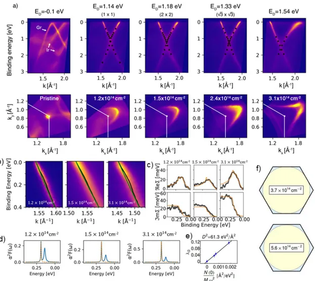
In Figure 1a we show ARPES spectra of pristine and Cs doped graphene. For each amount of
deposited Cs, we also have performed structural characterization by LEED (see supplemen-
tary information). Pristine graphene on Ir(111) (see Methods section for details pertaining
synthesis) has the R0 structural phase.
42This is confirmed by the moir´ e pattern observed
in LEED. The moir´ e pattern is a result of corrugations due to chemically modulated sub-
strate interaction.
43It hosts weakly covalently bonded regions with a small charge transfer
from graphene to Ir(111).
43Using ARPES (Figure 1a) we find in agreement to previous
Figure 1: (a) ARPES scans of Cs doped graphene/Ir(111) in the ΓKM direction (top panel)
and Fermi surface maps (bottom panel) for different Cs coverages. The shift of the Dirac
point is indicated in the top panel and the carrier concentration of graphene per cm
2is
indicated in the bottom panel. (b) High-resolution ARPES data in the vicinity of the kink
feature along the ΓK direction. Black and green lines denote ARPES intensity maxima and
the bare band, respectively. (c) Real and imaginary part of the self-energy (denoted as ReΣ
and ImΣ) for different doping levels. (d) Eliashberg functions (blue) and contribution of
the G band phonon (orange) along ΓK as a function of carrier concentration. The orange
lines in panel (c) denote the self-energy functions that are calculated from these Eliashberg
functions. (e) Fit of the deformation potential D
2(see text for details). (f) Tight-binding
calculation of the Fermi surfaces of doped graphene (blue regions) for carrier concentrations
just before and beyond the Lifshitz transition.
literature
42,44that R0 graphene/Ir(111) is only weakly hole doped. After depositing Cs onto the sample surface at room temperature, we find that the moir´ e pattern observed in LEED disappears and only the first order diffraction spots are left. This LEED pattern is denoted as 1 × 1 in the following. The disappearance of the moir´ e pattern upon Cs deposition is an indication of a change in the graphene-substrate interaction. The graphene-Ir(111) in- teraction also manifests in minigaps
44which are visible in the ARPES spectrum as regions of weaker π band intensity. After Cs deposition, these minigaps disappear, indicating that Cs doping weakens the local variations in the graphene-Ir(111) interaction. We expect that the charge transfer to graphene becomes homogeneous and removes the hybridization of C and Ir bands. ARPES also confirms a single doping phase as only one Dirac cone is visible.
Increasing the Cs amount, we are able to reach an ordered 2 × 2 phase of Cs on graphene as reported previously.
45This phase also has a single Dirac cone in ARPES. Analysis of the experimental Fermi surface from ARPES measurements yields a carrier concentration of n = 1.5 × 10
14cm
−2. Further increasing Cs deposition leads to the √
3 × √
3 phase in LEED and a slightly higher doping level. Here we have n = 2.4 × 10
14cm
−2. In order to confirm the ARPES derived carrier densities by another method, we also performed Fourier transform scanning tunneling spectroscopy (FT-STS) measurements
41(see supporting in- formation). These indicate carrier concentrations of 1.7 × 10
14cm
−2for the 2 × 2 phase and 1.9 × 10
14cm
−2for the √
3 × √
3 phase. The carrier concentration for the 2 × 2 is in excellent agreement to the value from ARPES and to previous experiments
45. However, the concentration for the √
3× √
3 phase from FT-STS is lower by a factor ∼ 1.3 when compared to ARPES. This can be understood by the √
3 × √
3 phase corresponding to graphene fully intercalated with Cs. Any extra Cs lies on top of graphene and a system with small amounts of extra Cs on top still shows a √
3 × √
3 diffraction pattern in LEED. Thus the √ 3 × √
3
phase exists for a broader range of adsorbate concentrations and can slightly vary from sys-
tem to system. Thus LEED is a good measure of stoichiometry for the 2 × 2 phase only. In
order to ensure depositing of equal Cs amounts in the Raman and ARPES investigations,
we calibrated the deposited Cs using a quartz microbalance as a multiple of the amount of Cs needed for reaching the 2 × 2 phase. Since the 2 × 2 phase is well defined, this approach yields reproducible sample stoichiometries for different samples and in different experimental setups.
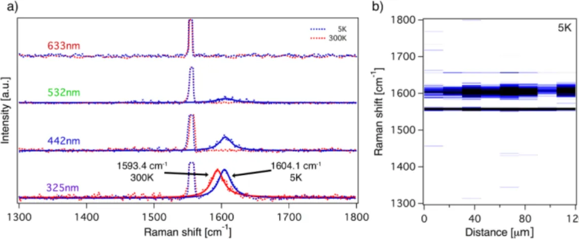
Figure 2: (a) Ultra-high vacuum (UHV) Raman spectrum of pristine graphene/Ir(111) at T =5 K and T =300 K for four different laser wavelengths in the range between red and ultraviolet. The dashed lines denote the experimental data and solid lines Lorentzian fits.
The G band taken at 325 nm excitation shows an upshift in frequency upon cooling (indicated by arrows in the lower panel). The sharp line at 1555 cm
−1is due to oxygen in the unavoidable part of the laser path outside the vacuum (see supporting information Figure S1 for a sketch of the UHV Raman setup). (b) Linescan of the Raman spectrum (at 325 nm) across a 120 µm distance of the sample.
Evaporation of excess Cs onto the sample does not result in an ordered phase according
to LEED but it is still possible to increase the graphene doping level. At n = 3.1 × 10
14cm
−2(see Figure 1a) we already see marked deviations from the usually observed trigonal warping
in ARPES. As is shown in Figure 1a (bottom row), the warping direction changes from con-
vex to concave. We are able to reach a value of n = 4.4 × 10
14cm
−2(For the highest value of
n, see supplementary information). Regarding the relation between Cs/C stoichiometry and
carrier concentration, we note that each Cs atom may donate less than one electron. How-
ever, this does not affect the carrier densities determined from ARPES because this method
is not dependent on the stoichiometry but directly measures the carrier concentration of
graphene from the area of the Fermi surface of graphene.
Let us now turn to the analysis of electron-phonon coupling. Figures 1b depicts high res- olution scans of the “kink” feature at low binding energy. We first perform a standard self-consistent self-energy analysis
7–9of ARPES data in the kink region yielding the complex self-energy and the Eliashberg function. These are depicted in Figures 1c and 1d, respec- tively. By integrating the Eliashberg function of graphene
8in the region of the G band, we obtain λ
G, the electron-phonon coupling constant for the G mode that is frequently used in ARPES literature. The Raman community often expresses electron-phonon coupling by the deformation potential D
2. The deformation potential and the electron-phonon coupling constant λ
Gare connected as λ
G= N (0)D
2/(M ω
2) (see Ref. 19). Here N (0) is the electron density of states per unit cell, per eV and per spin at the Fermi level, M the carbon mass and ω the G band frequency. The resulting fit of four charge carrier concentrations is depicted in Figure 1e and yields D
2= 61.3 eV
2/ ˚ A
2. Finally, Figure 1f depicts a tight-binding cal- culation of the Fermi surfaces at carrier concentrations just before and beyond the Lifshitz transition. In this Figure we show Fermi surface contours at n = 3.7 × 10
14cm
−2and at n = 5.6 × 10
14cm
−2. For the higher concentration of n = 5.6 × 10
14cm
−2, we are already above the Lifshitz transition (i.e. the Fermi surface is a single contour) while the lower con- centration is just before the Lifshitz transition (i.e. the Fermi surface consists of two contours that almost touch). For the calculation of these Fermi surface contours we have employed a third-nearest-neighbor tight-binding model
46where the matrix elements are fitted to the experimental ARPES band structure. It is clear that the carrier concentration at which the Lifshitz transition happens, is in between these two concentrations. Using the same tight- binding model, we estimate a value of n = 4.4 × 10
14cm
−2where the Lifshitz transition is observable by resonance Raman. We expect that the Lifshitz transition is induced purely by doping because we do not observe a lattice deformation. This is corroborated by the diffraction pattern of an overdoped sample above the √
3 × √
3 phase to a doping level close
to the Lifshitz transition. The diffraction pattern of this sample [shown in the supporting
information in Figure S2(e)] still shows sharp spots in a hexagonal pattern that are due to
graphene.
Raman spectrum of epitaxial graphene/Ir(111)
In Figure 2 we show the Raman spectra at T=300 K and at T=5 K of epitaxial graphene/Ir(111) measured by lasers with wavelengths 633 mm, 532 nm, 442 nm and 325 nm. The depicted spectra are the average over 25 points chosen along a scan across 120µm on the surface. In principle, for interpretation of the observed temperature-dependent spectra, in-plane strain and wrinkle formation due to the different thermal expansion coefficient of graphene and the Ir substrate must be considered.
47–49Only the ultraviolet (UV) laser (325 nm) results in a strong Raman signal at room temperature. Upon cooling, the spectra taken by 532 nm and 442 nm excitation show a weak Raman signal which could be a sign of temperature induced changes in the substrate interaction. These observations extend previous works reporting the absence of a Raman signal for graphene/Ir(111) that belongs to the R0 structural phase for visible excitation at room temperature.
42So far, no quantitative explanation regarding the absence of a Raman signal for visible laser excitation for R0 graphene on Ir(111) has been given. We speculate that it could be explained in terms of minigaps
44which appear at certain energies in the band structure. It has been shown by ARPES that the minigaps are in all directions around K point and close nowhere.
50If the laser energy hits a minigap, no electrons can be excited between the valence and conduction π bands of graphene and the Raman intensity is supressed. The high quality of graphene is also corroborated by the absence of a defect related D peak. Interestingly the 2D peak is absent in all measurements.
This observation is in agreement to previous works and might be related to the short life- time of photoexcited charge carriers in graphene adsorbed on metals which supress the 2D intensity.
51Temperature induced strain in epitaxial graphene
Let us now move to the Raman analysis of strain
52,53induced by the temperature depen-
dent change in the lattice constant. For epitaxial graphene on Ir, the thermal expansion of
graphene essentially follows the substrate.
54The nonlinearity in T of the thermal expansion
coefficient α(T ) of iridium must be taken into account.
55,56To accurately describe the ex- pansion of the Ir substrate in the temperature range explored (5 K−300 K), we fit α(T ) to literature values
55,56and calculate the expansion as l
0/l = exp( R
α(T )dT ). Here l
0and l are the lattice constants at temperatures corresponding to the upper and lower border of the integral, respectively. For describing the Ir lattice expansion of the present experiment, the integral above is taken from T = 5 K to T = 300 K. The strain in per cent is calculated as 100(l
0/l − 1) yielding = 0.134%. The phonon downshift corresponding to is given by
∆ω = −2ω
0γ (see Ref. 57 and references therein). Here γ = 1.99 (Ref. 57) is the Gr¨ uneisen parameter of the doubly degenerate G phonon mode of graphene, ω
0= 1606.5 cm
−1is the phonon frequency at 5 K. These values yield a strain induced downshift of the G band phonon when going from 5 K to 300 K of ∆ω = −8.6 cm
−1which is in excellent agreement to the experimental value of ∆ω = −10.7 cm
−1.
Figure 3: (a) Ultra-high vacuum (UHV) Raman spectra of Cs doped epitaxial
graphene/Ir(111) with increasing carrier concentration from left to right measured by four
laser lines. The raw data (dots) of the Raman G band together with a Fano lineshape fit
are shown. (b) UHV ultraviolet Raman spectra of doped graphene with increasing carrier
concentration measured with 325 nm excitation. All Raman spectra are taken at T =5 K
and a vacuum better than 2 × 10
−10mbar. (c) Calculated Raman spectra for 325 nm light
excitation and identical carrier concentrations as in (b).
Raman spectrum of Cs doped graphene/Ir(111)
We have used a Fano lineshape
30,36,58,59to fit the G band Raman spectra for all doping levels by
F (ω) = I
0(1 +
ω−ωqγ/20)
21 + (
ω−ωγ/20)
2. (1)
Here I
0is the Raman intensity, ω
0the line position, γ the full width at half maximum and 1/q the asymmetry (or Fano) factor which describes the strength of the interference effect between the discrete and continuous spectra. For 1/q = 0, we have a Lorentzian lineshape indicating no interference effect. In the following we analyze the carrier concentration de- pendence of I
0, ω
0, γ and 1/q. Figure 3a illustrates that, upon evaporation of Cs onto the sample, the observed Raman spectra dramatically change compared to those of pristine graphene. For the first deposition of Cs all laser energies except the red laser (633 nm) yield a finite Raman intensity. We attribute the appearance of a Raman signal to removal of the hybridization of the graphene and Ir states as discussed in the ARPES section. From Figure 3a we observe that the Raman intensity almost vanishes for the green (532 nm) laser at a carrier concentration of 2.4×10
14cm
−2(corresponding to the √
3 × √
3 phase). The Raman intensity for the blue laser (442 nm) vanishes at a doping level of 3.1×10
14cm
−2. On the other hand, the UV laser (325 nm) yields a Raman spectrum up to the highest doping level. This can be understood in terms of the condition that light can only induce transitions across the Dirac cone between occupied states in the valence band and unoccupied states in the conduction band. If doping shifts the Fermi level deep into the conduction band, these transitions are forbidden by Pauli blocking. The UV laser always fulfills the resonance con- dition 2E
F> E
lasersince its laser energy (E
laser=3.8 eV) is significantly higher than twice the maximum Fermi level shift (E
F= 1.58 eV from the ARPES data of maximally doped graphene).
Figure 3a also reveals that the Raman spectrum taken with the lowest photon energy for each
doping level becomes Fano-like. This applies to the 532 nm (green) laser for 1.5×10
14cm
−2,
the 442 nm (blue) laser for 2.4×10
14cm
−2and the UV laser for 3.1×10
14cm
−2. The most
striking feature is that the Fano tail of the present data is towards higher wavenumber with respect to the peak position. This corresponds to a positive sign of 1/q. The origin of this unusual Fano lineshape will be explained in the next section. In Figure 3b we show UV Raman spectra with increasing carrier concentration. The position of the G peak shifts to- wards higher phonon energies for carrier concentrations up to 1.5×10
14cm
−2before it shifts down. The UV Raman spectrum allows for comparison of the G line position of pristine (1606.3 cm
−1), weakly doped graphene (1615.9 cm
−1for the lowest Cs deposition) and fully doped graphene (1550.0 cm
−1). A key to understanding the present results is the interference of the electronic and vibrational Raman which also plays a major role in explaining the Fano asymmetry in carbon nanotubes.
28Here we apply this theory
30, using the experimental band structure of graphene derived from ARPES measurements. The calculated Raman spectra are depicted in Figure 3c and a very good agreement regarding the position and Fano asym- metry can be seen. In the following section we will show a quantitative comparison between experiment and theory regarding the position and asymmetry of the G band and discuss the details of the Raman calculation. Let us now look to the temperature dependent Raman spectra of doped graphene. This is motivated by question if intercalation of Cs liberates graphene from the substrate, so that it does not follow any more the lattice constant of Ir.
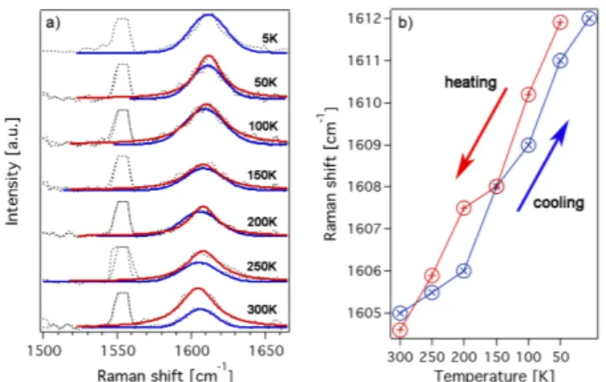
The corresponding Raman spectra and the G band positions are shown in Figure 4. An upshift of the G band position by 7 cm
−1with decreasing temperature (from 300 K to 5 K) is found. This is within the experimental accuracy to what we observed in Figure 2 for pristine graphene/Ir. Thus, despite Cs is intercalated in between graphene and Ir(111), the graphene still follows the compression of the underlying Ir substrate.
Discussion
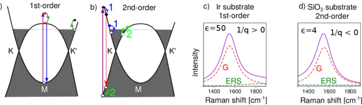
Electronic Raman scattering
In the electronic Raman scattering, the photoexcited electron and hole couple to electronic
Figure 4: (a) Temperature dependent Raman spectra of the √ 3 × √
3 phase of Cs doped graphene for a cooling and a warming-up cycle. (b) Raman peak positions as a function of temperature.
excitations via the Coulomb interaction and can generate one or more electron-hole pairs.
The large density of states in heavily doped graphene around the M point enhances the cross section for electronic Raman scattering. In the Figure 5(a,b) we graphically depict the relaxation processes which we consider in the calculation. We consider first order (creation of one electron-hole pair) and second order (creation of two electron-hole pairs) processes. The Coulomb interaction is affected by the dielectric screening of the substrate which is strong for the Ir substrate ( = 50)
60. As a consequence, only the first-order process (wavevector q = 0) is dominant for Ir. This is depicted in Figure 5c. We note that this first-order process excites an intraband electron-hole pair whose Coulomb interaction is maximum at wavevector q = 0. This process is completely different from the interband electron-hole pair excitation in the low doping regime, in which the direct Coulomb interaction vanishes at q = 0
31.
Interference between the first-order electronic Raman scattering (ERS) (shown by the
green line) and the G band (red line) produces the asymmetric Fano lineshape towards
larger wavenumber (1/q > 0). Figure 5d depicts the simulated Raman spectra of highly
doped graphene on SiO
2substrate. Due to the relatively weak screening effect ( = 4), the
second order Raman (q 6= 0) process overcomes the first-order process thanks to the double
resonant effect. The resulting Raman spectra are asymmetric towards the lower wavenumber
(1/q < 0). The spectra reported for doped graphene on Si have the Fano tail towards low wavenumers
27,36,37corresponding to negative values of 1/q. Our calculated results can thus fully explain the present data on Ir and the literature data on silicon wafers and other insulators.
Figure 5: (a) In the first-order electronic Raman scattering (ERS) process, an electron is excited to a virtual state above the saddle-point energy and then relaxes via Coulomb inter- action by exciting an e-h pair. When the electron recombines with the hole, the scattered energy is resonant to the M point energy. (b) In the second-order ERS process the photoex- cited e-h pair occupies a real state. The electron and hole relax to lower energy states by exciting two e-h pairs near Fermi surface with oppposite momenta. Calculated Raman spec- tra of highly doped-graphene on (c) Ir substrate and (d) SiO
2substrates. The dashed lines indicate the spectral contributions of the vibrational Raman scattering by the G phonon and ERS. The solid line is the spectrum after considering interference between these two contributions.
G band position: experiment and theory
In Figure 6a, we show plots of the experimental G band positions versus carrier concentration and along with a calculation of the phonon energy shift with carrier concentration. We quantitatively describe the observed Raman G band shifts by considering the effects of phonon renormalization and lattice expansion
5. Our model is based on expressing the doping induced change of the Raman G band frequency ∆ω as a sum of static (lattice expansion) and dynamic (electron-phonon coupling) effects as ∆ω = αω
static+ ω
dynamic(D
2) (Ref. 5).
Here α is a parameter that describes the scaling of the theoretical doping dependence for
freestanding graphene due to the effects of the Ir substrate. We have shown in Figure
2 (temperature dependence) that the lattice constant of graphene perfectly follows the Ir
affected and hence α 6= 1. D
2is the deformation potential as explained in the ARPES section. The equations for ω
staticand ω
dynamicare given in the Methods sections. Using the ARPES-derived value of D
2= 63.1 eV
2/˚ A
2, we proceed to perform the fit of the parameter α describing the lattice expansion versus carrier concentration. We find α = 0.18 which would suggest there is still compressive strain, i.e. the lattice constant of freestanding graphene doped to an equal concentration would be larger. Let us discuss these results for D
2and α in more detail. First, the experimental value of D
2is considerably larger than the DFT value of D
2= 45.6 eV
2/˚ A
2(Ref. 5). A perfect agreement between theory and experiment is achieved by GW calculations which yield D
2= 62.8 eV
2/˚ A
2(Ref. 61). This can be understood by the fact that the underlying electron and phonon dispersions of graphene are accuratly described only by GW calculations and DFT underestimates the size of the electron and phonon dispersions.
61Regarding the dependence of the αω
staticterm that describes the lattice expansion on carrier concentration, we estimate from Figure 6a that the observed maximum G band frequency downshift from undoped graphene is ∼50 cm
−1. Assuming that 69 cm
−1downshift of the G band phonon corresponds to 1% expansive strain (Ref. 57), we estimate a C-C bond increase of 0.8%. Indeed, this is close to what has been observed by diffraction in intercalated graphite where the C-C bond length increases from 1.4211˚ A (pristine graphite) to 1.4320˚ A (stage 1 GIC)
62corresponding to a 0.7% increase in the lattice constant. The small differences to the present case could be ascribed to the higher doping level that we have achieved in the present case corresponding to a shift of the charge neutrality point to E
D= 1.58 eV whereas the stage 1 KC
8GIC has E
D= 1.35 eV.
63. Interestingly, the theoretically expected downshift for the carrier concentrations achieved is much larger which is described by α = 0.18. We attribute this to two effects. First, the substrate interaction is strong despite Cs is intercalated in between graphene and the substrate. This is evident from the temperature dependent Raman spectra of the √
3 × √
3 phase where the C-C lattice
constant is following the Ir substrate. It is clear that the substrate interaction can hinder the
lattice expansion which would result in α < 1, as we have observed. Additionally substrate
interaction can cause the formation of wrinkles. Second, regarding the very large difference between experiment and theory, the analytical expression for ω
staticis derived from DFT calculations and perhaps not sufficiently accurate to describe the very high doping levels considered here.
5Next, let us discuss how our observed G band shift corresponds to experiments performed with ionic liquid gated graphene (data from Ref. 15). These data are shown in Figure 6a along with our experiments. The ionic liquid gated graphene on Si oxide has a maximum upshift of 25cm
−1(Ref. 15) whereas the observed maximum G band upshift of Cs doped graphene on Ir is about 10 cm
−1. Notably, Rb doped graphene on Si oxide also displayed a maximum upshift of the G band by 25cm
−1(Ref. 37) and it could therefore be related to the substrate. We believe that the observed differences in the slope of the G band with doping lie in the phonon dispersion relation of graphene on insulators and on metals. It has been put forward, that for graphene on metals, the Kohn anomalies at Γ and K points are screened by the metal substrate
64. High resolution electron energy loss spectroscopy measurements and calculations of the phonon dispersion relations of the graphene/Ir(111) system
65indicate that the Kohn anomaly at Γ is not as strongly kinked than in freestading graphene. This results in a higher phonon frequency for graphene/Ir(111) compared to freestanding graphene. Upon doping, the Kohn anomaly at Γ point shifts away to a finite wavevector equal to 2k
F(k
Fis length of the Fermi wavevector) and the Γ point phonon frequency moves to higher values. Thus, for graphene on Ir, the upshift in phonon energy as a result of doping is smaller than the one observed for freestanding graphene. These arguments explain the experimental data of graphene/Ir(111) and graphene/Si oxide shown in Figure 6a.
Doping dependence of Fano asymmetry and spectral linewidth
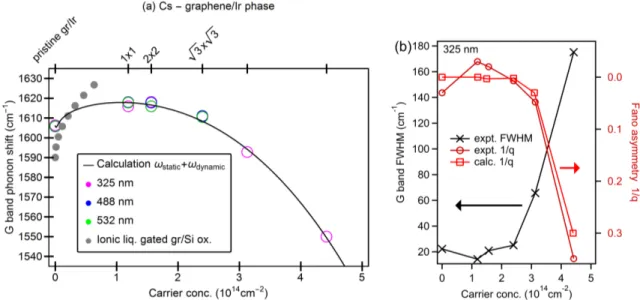
Figure 6b depicts the experimental and theoretical Fano asymmetry parameter 1/q and the
experimental spectral width (FWHM) as a function of carrier concentration. The values of
Fano asymmetry 1/q and the FWHM at carrier concentrations larger than 3 × 10
14cm
−2exhibit a strong deviation from the behaviour at lower carrier concentrations. Correlating this with the experimental Fermi surfaces from ARPES, we attribute the sudden increase in 1/q and line width to increased electronic Raman scattering as the Lifshitz transition is approached. This is not only via the large carrier concentration which causes the downshift of the G band position but also via the change in the energy-momentum conservation for electron-hole pair excitation affecting the Fano lineshape of the G band as theoretically predicted
30.
Figure 6: (a) Raman G peak positions of Cs doped graphene versus the carrier concentration.
The full line is a model calculation of the G band frequency (see Methods section) and open circles are the experimentally determined G band maxima. The grey filled circles indicate the G peak position from ionic liquid gated graphene on fused silica (Ref. 15). (b) Crosses connected by a black line: expt. linewidth (full width at half maximum) of the Raman G peak. Circles connected by a dark red line: the experimental Fano asymmetry factor obtained from measurements with the UV (λ=325 nm) laser. The squares connected by a red line are the calculated values of the Fano asymmetry (obtained by fitting a Fano line to the calculated spectra in Figure 3c).
Conclusions and outlook
In conclusion, we have established a fully experimental relation between energy shift and
Fano asymmetry parameter of the Raman G band versus carrier concentration in doped epi-
taxial graphene. This is based on ARPES experiments that reveal the deformation potential D
2from the kink feature and Raman measurements on identical samples. This relation is expected to be useful for future stand-alone UHV Raman experiments. In the Raman exper- iments we have exploited the band renormalization upon doping which reduces the optical transition energy at the saddle point. This allowed us to achieve resonance Raman condi- tions with UV light in the vicinity of the van Hove singularity. We have observed a peculiar Fano lineshape with an asymmetry tail towards high Raman shifts. This is opposite to what is known for doped graphene on semiconductors such as Si oxide. By performing resonant Raman calculations, we have fully explained this behaviour by considering first and second order electronic Raman contributions.
Our work has introduced UV UHV Raman spectroscopy as a function of temperature as a versatile tool for surface science of two-dimensional materials. Let us now consider two future research directions. First, the presented approach could also be applied to hole doped graphene. Theoretically, we expect it to yield qualitatively similar results if the Fermi level reaches the van-Hove singularity in the valence band. Hole doping of graphene on Ir(111) has already been achieved by oxygen intercalation
66or chlorine intercalation
67and it would be interesting to investigate such samples by UHV Raman spectroscopy at low temperatures.
Second, UHV Raman spectroscopy of alkali doped graphene could be used for investigation
of the superconducting properties of graphene analogous to previous experiments that are
carried out on superconducting bulk CaC
6(Ref. 68). In these experiments, a sharp super-
conducting coherence peak is observed by Raman at 24 cm
−1which is very close to the value
for the superconducting gap obtained by scanning tunneling spectroscopy (25.8 cm
−1) high-
lighting that this Raman peak has its origin in the superconducting phase.
68For graphene,
electronic Raman scattering from the superconducting phase has not been observed yet. It
should also lead to low-energy Raman peaks with an energy roughly equal to the size of
the superconducting gap.
69Theory predicts that this holds for both, s-wave and d-wave
superconducting graphene at doping levels close to what is shown in the present work.
70The Raman intensity of these low-energy peaks has been estimated to be approximately a factor 1000 lower than the G band intensity.
69Given, the comparably low Raman intensity of graphene on metals with respect to graphene on insulators, we estimate that the electronic Raman peaks at low wavenumber will be hard to measure for the present graphene/Ir(111) system. An approach for addressing this problem is to carry out the present experiment with graphene transferred onto an an insulating substrate. The large Raman response of graphene on insulators compared to graphene on metals could be a key to measure the ap- pearance of low wavenumber Raman peaks when the temperature is below T
c. Thus, a future experiment could be to perform doping graphene into the superconducting state after it is transferred onto an insulator. Having doped graphene on an insulator inside UHV would in principle also allow for electrical transport characterization. To that end, the presented UHV Raman setup can be extended via electrical feedthroughs into the UHV chamber. In such a setup, the Raman spectrum and the four-point resistance could be measured simultaneously as a function of alkali doping. This could provide strong evidence for the existence of of a superconducting phase and elucidate its Raman response. Finally, such a work could also be extended to doped bilayer graphene with a relatively higher critical temperature
21and doped heterostructures composed out of different van-der-Waals materials.
Methods
Synthesis
Graphene/Ir(111) has been synthesized in-situ in the preparation chamber attached to the
UHV Raman system, using an established recipe
71that yields monolayer coverage by a self-
limiting process.
72The fact that we have monolayer graphene is supported by three tech-
niques: ARPES, STM and LEED. ARPES spectra show only one π valence band. A bilayer,
e.g. would show two π valence bands. We have also verified that the full Ir(111) is covered by
monolayer graphene via scanning the spot of the ARPES measurement (spotsize: 100×50
µm
2) over the full 1×1 cm
2Ir(111) crystal. We have nowhere found two valence bands which would hint bilayer formation. The STM images that we took of samples prepared in that way (supporting information Figure S4) show the moir´ e pattern due to substrate interaction. This moir´ e pattern is a clear proof of monolayer coverage. Also, the individual carbon atoms of the monolayer are clearly seen. Finally, the LEED shown in Figure S2 of the supporting information displays the diffraction spots due to the moir´ e pattern of monolayer graphene/Ir(111). The Ir(111) single crystal which was used as a substrate for the graphene synthesis which was first sputtered (1 keV) in Ar atmosphere (1 × 10
−6mbar) followed by an annealing step under O
2flow (1×10
−7mbar) at 1200
◦C for 30 mins. When the crystal cooled down to room temperature a rapid flashing to 1700
◦C provided a clean surface indicated by a sharp hexagonal LEED pattern. For the graphene synthesis we used a combination of CVD (chemical vapor deposition) and TPG (temperature programmed growth). Hereby propene (C
3H
6) was dosed into the UHV chamber (1 × 10
−6mbar) for 60 s at room temperature to adsorb molecules on the iridium surface followed by a flashing step to 1250
◦C for 3 min without propene to create graphene islands with the same crystallographic orientation as the substrate. The TPG synthesis was applied twice to increase the amount of graphene islands.
After the second TPG step the sample was not cooled down to room temperature but only to 900
◦C. After reaching this temperature, the CVD growth was carried out. Hereby propene was dosed (1 × 10
−6mbar) for 15 min to grow graphene in the areas between the islands creating a closed monolayer of graphene without rotational domains with respect to iridium.
Finally the sample was cooled down slowly to room temperature to minimize the formation
of wrinkles. Cs was deposited by evaporation from a commercial SAES getter source. The
evaporated amount of Cs was calibrated by a quartz crystal microbalance. The amount of
evaporated Cs monolayer reported in the paper are with respect to the bulk Cs structure.
Angle-resolved photoemission spectroscopy
ARPES was performed at the BaDElPh beamline
73of the Elettra synchrotron in Trieste (Italy) with linear s- and p- polarisation at hν = 31 eV at temperatures of 20 K. The graphene/Ir(111) samples were prepared in-situ and measured in a vacuum better than 5×10
−11mbar. Immediately after the synthesis, Cs deposition was carried out in an ultra-high vacuum (UHV) chamber from SAES getters with the sample at RT. We performed stepwise evaporation of Cs which we monitored by ARPES measurements of the band structure. Cs evaporation was stopped after the desired doping level was reached.
Scanning Tunneling Spectroscopy and Microscopy
STM and STS are carried out with a background pressure lower than 10
−11mbar. The constant energy maps are recorded using the lock-in technique with a modulation frequency of 833.1 Hz and a modulation amplitude of 8 mV, providing an energy resolution of 14 meV.
An etched tungsten tip is used for all measurements, which is prepared in situ by applying positive or negative voltage pulses up to 10 V. Fourier transformed images are obtained from spectroscopic maps by using the fast Fourier transform of the SPIP software
74with Hanning window. Subsequently, the symmetry of the sample is exploited to enhance the signal to noise ratio.
Ultra-high Vacuum Raman Spectroscopy
UHV Raman measurements were performed in the back-scattering geometry using commer-
cial Raman systems (Renishaw) integrated in a homebuilt optical chamber
75, where the
exciting and Raman scattered light were coupled into the vacuum using a 50x long-working
distance microscope objective with an NA of ∼0.4 and a focal distance of 20.5 mm for lasers
with wavelength 442 nm, 532 nm and 633 nm. For the UV laser, UV compatible optical
elements have been used. The 20x UV objective has a focal distance equal to 13 mm and
an NA=0.32. A sketch of our experimental setup is shown in the supplemental information.
The laser powers used were ∼2 mW for the UV laser and 9 mW, 25 mW and 45 mW for blue, red, and green lasers respectively. Assuming that this energy gets spread over ∼4 µm
2, we obtain power densities of 100 kW/cm
2. Using lHe cooling and given the fact that graphene is directly on a metal, these laser powers result in a linear dependence of Raman intensity to the laser power. The position of the laser on the sample could be checked by a camera in the laser path. All spectra have been calibrated in position and intensity to the O
2vibration at 1555 cm
−1(Ref. 76). O
2Raman peaks can be seen with all laser lines used in the present experiment which is consistent with the previous published works.
76,77Further precautions that we took in order to prevent laser heating induced effects is a study of the laser power dependence (see supporting information).
Calculations of the Raman spectra
Calculations of the doping dependent phonon shift
We have calculated the Raman shift ∆ω = αω
static+ ω
dynamic(D
2) according to the well- established model
5. The frequency downshift due to doping induced lattice expansion is described by ω
static. The parameter α is a scaling factor for the phonon downshift with respect to the calculated doping dependence of freestanding graphene. The frequency upshift is described by ω
dynamic(D
2). Here D
2is the deformation potential. For ω
staticwe use the equation for freestanding graphene (Ref. 5):
ω
static= −2.13σ − 0.0360σ
2− 0.00329σ
3− 0.226|σ|
3/2(2)
Here σ is the charge carrier density per cm
2and ω
staticis given in cm
−1. For calculation of the dynamic contribution, we need to consider
F e
qF(ω) = 2 N
X D
2( f e
km− f e
kn)
k,m−
k,n+ ~ ω + iδ . (3)
Here the sum goes over all points in the 2D BZ and f e
km= f (
km−
F) with f being the Fermi distribution function. For numerical integration, we have used a trigonal grid having
∼ 1000 points in the 2D BZ of graphene. ~ ω is the phonon energy of the undoped system and δ = 10 meV a small broadening term. For the band structure calculations we have used a third nearest neighor tight-binding fit to the experimental ARPES band structure.
46The corresponding dynamic shift is calculated by
ω
dynamic= Re
F e
0F(ω
0) − F e
00(ω
0) 2M ω
0. (4)
Here M is the free electron mass, ω
0the unperturbed phonon frequency of the G band and F e
0Fis defined in equation 3. In the calculations we used an artificially high temperature of T = 400 K in the Fermi distribution function as a means to describe doping inhomogeneities and charge puddles that can not be resolved spatially. A similar observation was made in previous works that have also used artificially high temperatures
37or Fermi level smearing
16.
Raman Intensity calculation
We consider the interference between the G band phonon Raman and electronic Raman scattering (ERS) pathways and write the Raman intensity as
I(ω
s) = [A
G(ω
s) + A
ERS(ω
s)]
2, (5)
where A
G= P
ν
A
ν, is the G phonon scattering amplitude which consists of zone center (Γ
point) ν = LO and iTO modes and A
ERSis the ERS scattering amplitude. The phonon Ra-
man process consists of (1) excitation of an electron-hole pair by the electron-photon interac-
tion, (2) phonon emission by means of the electron-phonon interaction, and (3) electron-hole
recombination and photoemission by the electron-photon interaction. Based on the three
sub-processes, phonon scattering amplitude is given by
78A
ν(E
s) = X
k
M
opvc(k)M
epν(k, k)M
opcv(k) [f (E
kv) − f(E
kc)]
[E
L− E
kcv− iγ/2][E
L− E
kcv− ~ ω
ν− i(γ + Γ
ν)/2][E
L− ~ ω
ν− E
s− iΓ
ν/2] . (6) Here E
Lis the laser energy, E
sis the scattered photon energy, E
kcv= E
kc− E
kvis the electron energy difference between the conduction (c) and the valence (v) bands at a wave vector k. The energy bands of graphene have been obtained by the tight–binding (TB) fits to the experimental band structure considering up to the three nearest–neighbors for each of doping level. The M
opand M
epνare the electron–photon and electron–phonon matrix elements, respectively. These matrix elements are obtained within the TB method.
79,80. The phonon frequency of the ν-th mode is depicted by ω
νand a broadening factor of the photoexcited carriers γ = 0.2 eV is used. The phonon linewidth Γ
νis fitted to the Raman measurements.
The summation of states considered in Eq. (6) are taken below a cut-off energy E
kcv= 5 eV.
For the ERS amplitude A
ERS, we consider the lowest order processes as shown in Figure 4. In the first-order ERS, the photo-excited carrier excites an electron-hole (e-h) pair via Coulomb interaction with zero momentum transfer (q = 0) or vertical transition. We note that the e-h pair is allowed to occupy a virtual state as the lifetime of Coulomb interaction is very short (∼ 10 fs). The first order ERS amplitude is given by
A
(1)ERS(E
s) = X
k
X
k0
M
opvc(k)K
kc,k0c,kc,k0c(0)M
opcv(k) [f (E
kv) − f(E
kc)]
[E
L− E
kcv− iγ/2][E
L− E
kcv− E
ke0− i(γ + Γ
e)/2][E
L− E
ke0− E
s− iΓ
e/2] ,
(7)
where E
ke0and Γ
e= 60 meV are the energy of the excited e-h pair and the Coulomb scattering
rate, respectively. If E
L> E
M(here E
Mis the M point transition energy), we expect that
the photoexcited electron relaxes to the conduction band at the M point. In such a way
we estimate E
s= E
M− E
ex, where and E
exis the exciton binding energy, estimated to be
100 meV. For E
L< E
M, we expect hot luminescence
15, i.e. the photo-excited carrier relaxes
to the lowest intermediate energy ∼ 2E
Fand then recombines with the hole by emitting
E
s≈ 2E
F. The direct Coulomb interactions between two electrons for initial states 1, 2 with states 3, 4 is given by K
1,2,3,4(q). In the TB approximation this kernel is expressed as
K
1,2,3,4(q) = X
ss0=A,B
C
s1C
s20C
s∗3C
s∗40v (q) /. (8)
Here C
siis the TB coefficient for the atomic site s at the state i and v(q) is the Fourier transform of the Ohno potential
81. is the dielectric constant of the substrate. Because the Raman shift of the ERS process is about 0.2 eV, we do not consider the dynamical screening effect. For the second order ERS, we consider the excitation of two e-h pairs by the photo-excited electron and hole [Figure 4(b)]. The amplitude of the second-order ERS process is given by
A
(2)ERS(E
s) = X
k
X
k0k00q