ELECTRONIC PROPERTIES OF TWISTED‐LAYER GRAPHENE SYSTEMS
A thesis submitted to attain the degree of DOCTOR OF SCIENCES of ETH ZÜRICH
(Dr. sc. ETH Zürich)
presented by
TOBIAS MARKUS RAPHAEL WOLF MSc ETH Physics, ETH Zürich
born on 16.08.1991 citizen of Germany
accepted on the recommendation of Prof. Dr. Johann W. Blatter
Prof. Dr. Oded Zilberberg Prof. Dr. Jose Lado Prof. Dr. Alberto Morpurgo
2021
Abstract
Crystals with two-dimensional lattice structure, such as graphene, can be obtained from bulk crystals, such as graphite, by peeling off atomically-thin layers held in place by weak interlayer van der Waals attraction. Stacking the resulting isolated layers onto a substrate or back together allows to design so-called van der Waals heterostructures. In this procedure, introducing a finitetwistangle between layers leads to a structural beating pattern, known as amoiréstructure, characterized by an intermediate length scale between atomic and mesoscopic systems. This dissertation addresses how the moiré pattern impacts the electronic properties in three different graphene-based twisted-layer systems of increasing complexity.
First, we investigate a graphene layer stacked on hexagonal boron-nitride (g/hBN), where the small mismatch in the respective lattice constants allows for a large-scale moiré pattern. Graphene is a semimetal with a linear energy-momentum relation defining two valleys at low energies, so-calledDirac cones, whereas hBN is a band insulator. Consequently, the low-energy band electrons of graphene experience the substrate layer hBN as weak moiré-periodic potential that rearranges the dispersion of the graphene-layer into minibands and opens band gaps due to elastic scattering.
We explore the general form of the moiré-induced potential compatible with the sym- metries of the superstructure and find a six-dimensional parameter space. As a last step in this project, we then classify this parameter space through symmetries, band inversions and valley-topological gaps in the corresponding minibands. We find the conditions under which the moiré-induced potential can lead to anomalous transport signatures in valley Hall experiments.
Second, we consider twisted bilayer graphene, which is a stack of two identical graphene layers with a small relative angle. The moiré-periodic potential induces elastic interlayer hybridization between band electrons of one layer with those of the other. The resulting minibands are highly sensitive to the geometric tuning of the twist angle, and can (at specific angles) even lead to flat bands. The latter have small kinetic energy such that interactions will lead to strong correlations effects. We show that this effect happens at a twist angle𝜃∗=0.8◦for flat bands away from the charge neutral energy. When the system is doped with±6electrons per moiré cell, these bands are half-filled and electronic interactions produce a symmetry-broken ground state with localized spin moments that order ferromagnetically. We further show that applying an interlayer electric field quenches the magnetic order by in- troducing valley-dependent dispersion. With these results, we propose a solid-state platform that realizes electrically tunable magnetic correlations.
Third and last, we study twisted bilayer graphene stacked between magnetic insu- lators. Proximity to the latter introduces magnetic exchange and spin–orbit cou- plings in graphene, that can hybridize the spin degree of freedom. We show that a stacking can be engineered in a way that two overlapping flat minibands arise,
one for each valley. We predict that, at half-filling of these bands, Coulomb inter- actions lead to strong valley correlations. We find that these correlations prefer valley-mixing through anisotropy, have non-collinear spiral-order tendencies, and can again be tuned electrically through interlayer bias. We propose experimental sig- natures through anomalous transport in valley Hall experiments. With these results, we introduce a new engineered material where emergent, nontrivial valley physics substitutes spin physics.
Kurzfassung
Kristalle mit zweidimensionaler Gitterstruktur, wie z.B. Graphen, können aus Volu- menkristallen, wie z.B. Graphit, durch Abziehen atomar dünner Schichten, die durch schwache van-der-Waals-Anziehung zwischen den Schichten festgehalten werden, gewonnen werden. Das Stapeln der so entstandenen isolierten Schichten auf ein Substrat oder wieder zusammen ermöglicht den Entwurf so genannter van der Waals- Heterostrukturen. Bei diesem Verfahren führt die Einführung eines endlichenVer- drehungswinkelszwischen den Schichten zu einem strukturellen Schwebungsmuster, einer so genanntenMoiré-Struktur, die durch eine intermediäre Längenskala zwis- chen atomaren und mesoskopischen Systemen gekennzeichnet ist. Diese Disser- tation befasst sich mit der Frage, wie das Moiré-Muster die elektronischen Eigen- schaften in drei verschiedenen graphenbasierten Drehlagensystemen zunehmender Komplexität beeinflusst.
Erstens untersuchen wir eine einzelatomare Schicht von Graphen aufgebracht auf das Substrat hexagonales Bornitrid (g/hBN), wo ein eine kleine Diskrepanz zwis- chen den Gitterkonstanten ein langwelliges Moiré-Muster ermöglicht. Graphen ist ein Halbmetall mit einer linearen Energie—Impuls-Beziehung, sogenannten Dirac-Kegeln, die bei niedrigen Energien zwei Senken, oder “Valleys”, definieren.
Das Material hBN hingegen ist ein Bandisolator. Folglich erleben die niedrig- energetischen Bandelektronen in Graphen die Substrat-Schicht hBN als schwaches, Moiré-periodisches Potential, welches aufgrund elastischer Streuung die Dispersion der Graphenschicht in Minibänder umorganisiert und Bandlücken öffnet. Wir erkunden die allgemeine Form des Moiré-induzierten Potentials gemäss kompatibler Symmetrien der Superstruktur, und erhalten einen sechsdimensionalen Parameter- raum. Wir klassifizieren diesen Raum durch Symmetrien, Bandinversionen und Valley-topologische Lücken in den entsprechenden Minibändern. In einem letzten Schritt bestimmen wir die Bedingungen unter denen das Moiré-induzierten Potential anomale Transportsignaturen in Valley-Hall-Experimenten verursachen kann.
Zweitens betrachten wir zweilagiges Graphen mit Twist-Winkel, das aus zwei iden- tischen Lagen Graphen besteht, die einen kleinen relativen Drehwinkel zueinander haben. Das Moiré-periodische Potential verursacht elastische Streuung zwischen den Lagen, die die Bandelektronen einer Lage mit denen der anderen hybridisiert.
Die so folgenden Minibänder sind höchst empfindlich auf geometrische Feinabstim- mung im Twist-Winkel, was (bei speziellen Winkeln) sogar zu flachen Bändern führen kann. Letztere haben geringe kinetische Energie, sodass Wechselwirkungen starke Korrelationseffekte auslösen können. Wir zeigen, dass dieser Effekt bei einem Drehwinkel von 𝜃∗=0.8◦ eintritt, mit flachen Bändern bei Energien, die weg von der Ladungsneutralität liegen. Wenn das System mit±6Elektronen pro Moiré-Zelle dotiert wird, so sind diese Bänder halb gefüllt und Wechselwirkung erzeugen Symmetry-brechende Grundzustände mit lokalen Spin-Momenten, die sich ferromagnetisch ausrichten. Wir zeigen ausserdem, dass das Anbringen eines
transversalen elektrischen Feldes zwischen den Lagen eine Valley-abhängige Disper- sion erzeugt, welche die magnetische Ordnung abschwächt. Mit diesen Ergebnissen schlagen wir eine Festkörper-Plattform vor, in der elektrisch steuerbare magnetische Korrelationen umgesetzt sind.
Drittens und letztens studieren wir zweilagiges Graphen mit Twist-Winkel umgeben von Lagen aus magnetischen Isolatoren. Nähe zu letzteren induziert magnetis- che Austauscheffekte und Spin–Orbit-Kopplungen in Graphen, welche den Spin- Freiheitsgrad hybridisieren können. Wir zeigen, dass dieses mehrlagige System so konstruiert werden kann, dass zwei überlappende flache Minibänder erzeugt werden, jeweils eins pro Graphen-Valley. Wir sagen voraus, dass wenn diese Bänder halb gefüllt sind, Coulomb-Wechselwirkungen zu starken Valley-Korrelationen führen. Wir erhalten, dass diese Korrelationen den Valley-Freiheitsgrad mischen, d.h. Valley-anisotrop sind, die Tendenz haben nicht-kollineare Spiralordnung zu bilden, und wiederum durch ein transversales elektrisches Feld manipuliert wer- den können. Wir schlagen experimentelle Signaturen in anomalem Transport in Valley-Hall-Experimenten vor. Mit diesen Ergebnissen führen wir ein neuartiges Material ein, in welchem die wechselwirkungsbedingte, nicht-triviale Valley-Physik die Spin-Physik überschattet.
Abstract / Kurzfassung . . . i
1 Introduction 1 1.1 Discovery of graphene . . . 1
1.2 Graphene with a substrate-induced moiré structure . . . 2
1.3 Flat bands in twisted bilayer graphene . . . 4
1.4 Outline . . . 5
I Background 7 2 Graphene 9 2.1 Honeycomb lattice . . . 10
2.2 Tight-binding model and band structures . . . 11
2.3 Low-energy continuum approximation . . . 15
2.4 Topological aspects . . . 17
2.4.1 Berry curvature in the dynamics of band electrons . . . 18
2.4.2 Trivial and topological bands in monolayer graphene . . . 20
2.4.3 Topology of Dirac-like band crossings . . . 22
2.4.4 Valley topology and valley Hall response . . . 24
2.5 Zeeman and spin–orbit effects . . . 25
2.6 Electronic interactions . . . 28
2.6.1 Interactions in the tight-binding model . . . 29
2.6.2 Mean-field approximation . . . 29
2.6.3 Breaking of sublattice symmetry . . . 31
2.6.4 Magnetic frustration in triangular lattices . . . 33
3 Twisted graphene multilayers 35 3.1 Moiré superlattice . . . 35
3.2 Tight-binding model and minibands . . . 38
3.3 Low-energy continuum model . . . 40
3.3.1 Nearly-free band electrons . . . 40
3.3.2 Relation to the tight-binding model . . . 42
v
3.3.3 Single-valley bilayer moiré potential . . . 43
3.3.4 Single-valley monolayer moiré potential . . . 44
3.3.5 General aspects of twist-engineering . . . 47
II Twisted-layer systems 49 4 Dirac electrons and valley topology in g/hBN 51 4.1 Introduction . . . 51
4.2 Dirac-like particles in a periodic potential . . . 54
4.3 Bloch bands along𝜅–𝜇–𝜅0 . . . 59
4.3.1 𝐷3symmetry . . . 59
4.3.2 𝐶3symmetry . . . 60
4.3.3 Finite massΔ . . . 63
4.4 Berry curvatures and Chern numbers . . . 65
4.5 Valley-topological miniband insulator . . . 69
4.6 Conclusion . . . 71
5 Flat bands and magnetic correlations in TBG 73 5.1 Introduction . . . 73
5.2 Model and electronic minibands . . . 76
5.3 Effective triangular superlattice model . . . 78
5.4 Electronic interactions . . . 80
5.4.1 Rescaling the interaction strength along with the unit cell . . 80
5.4.2 Mean-field analysis . . . 81
5.5 Electric bias as valley flux . . . 83
5.5.1 Valley flux in the tight-binding model . . . 84
5.5.2 Valley flux in the low-energy model . . . 85
5.6 Interplay between interlayer bias and interactions . . . 86
5.7 Conclusion . . . 87
6 Flat bands and valley correlations in FI/TBG/FI 89 6.1 Introduction . . . 89
6.2 Model and electronic minibands . . . 91
6.3 Flat bands with spin-hybridization . . . 94
6.4 Effective triangular superlattice model . . . 95
6.5 Electronic interactions . . . 96
6.5.1 Mean-field analysis in the microscopic model . . . 96
6.5.2 Mean-field analysis in the effective model . . . 97
6.6 Artificial pseudospin–orbit coupling . . . 100
6.7 Tunable valley anisotropy . . . 102
6.8 Valley signatures . . . 102
6.9 Conclusion . . . 103
7 Summary and conclusion 105 Appendices 107 A Graphene 109 A.1 Valley operator in the tight-binding basis . . . 109
A.2 Commensurate moiré structure . . . 110
A.3 From inter-atom hops to a continuum moiré potential . . . 110
A.4 Gauge symmetry in the nearly-free Dirac-band model . . . 111
A.5 Analytical Berry curvature for band crossings . . . 112
A.5.1 Three-band crossing . . . 112
A.5.2 Two-band crossing: Anisotropic Dirac cone . . . 113
B Discretized Berry phase and Berry curvature 115 C Mean-field theory 117 C.1 Interacting many-body system . . . 117
C.2 Mean-field approximation . . . 117
C.3 Mean-field iteration . . . 118
C.4 Spin spirals . . . 119
D Hubbard model and Schrieffer-Wolf transformation 121 D.1 Fermi-Hubbard model . . . 121
D.2 Effective exchange interactions . . . 122
References 125
List of publications 141
Curriculum vitae 141
Acronyms 145
Acknowledgments 147
1
Introduction
In this chapter, we give an overview of the young but rich history of two- dimensional crystals that can be distinguished into several stages. We start with the discovery of graphene in 2004 through mechanical exfoliation and the quest to remove disorder and improve purity for better electronic properties. We then discuss the subsequent discovery of moiré superlattices in graphene on hexagonal boron nitride, that has lead to the first observable realization of magnetic subband splitting. Shortly after, an increasing number of other two-dimensional crystals were proposed and mechanically exfoliated, now systematically classified as van der Waals materials. Generally, these materials can be stacked together with (al- most) no chemical and geometric restrictions. This allows to systematically en- gineer moiré superstructures by controlling the twist angles, and can lead to flat bands at fine-tuned “magic” angles in various multilayer stacks. Such flat bands in presence of electron-electron interactions can exhibit phases with strong correla- tions and spontaneously broken symmetries. Indeed, when strongly-correlated in- sulting and superconducting states were first observed, it became clear that twisted van der Waals materials are well suited to engineer exotic correlated phases. At the end of the chapter, we provide an outline to this work.
1.1 Discovery of graphene
Two-dimensional (2D), single-layer crystals were initially believed to be unstable, first due to a physical argument by Peierls [1] in the 1930s stating that the diver- gent contributions of phonons destroy 2D crystalline order, and later due to a more general proof by Mermin [2]. However, both statements rely on the thermodynamic limit, and it turns out that two-dimensional crystals on the length scale of solar dis- tances are required before the logarithmic divergence becomes relevant [3]. In 2004, the synthesis ofgraphene[4], a single atomic layer of carbon, was the final confirma- tion that quasi long-range-ordered crystals exist in2D. The discovery of graphene
1
shaped experimental and theoretical condensed matter research so profoundly [5,6]
that, unsurprisingly, it was awarded with a Nobel prize only a few years later in 2010 – despite the apparent simplicity of the synthesis. Indeed, graphene can be extracted by putting a sticky tape on graphite, ripping off the top layers, and then identifying single-layer flakes under an optical microscope. This process is called “mechanical exfoliation”. There are several subtleties in this procedure, but essentially any ex- perimental group could develop this expertise and fabricate their own devices. This democratization of fabrication and the interesting electronic properties of graphene (and by now also of other 2D crystals) has started a new flourishing field of research.
Graphene has several unusual features [6,7], the most prominent of which is that the electronic band dispersion is semi-metallic at charge neutrality with linear band touchings (“Dirac cones”) in two valleys K and K’ in the Brillouin zone. As a result, the charge carriers in graphene can be described as condensed matter analogs of Weyl-Dirac Fermions. This leads to properties such as (i) an anomalous integer quan- tum Hall effect, (ii) suppressed back-scattering through potential barriers (pseudo- spin conservation, Klein-tunneling), and (iii) universal optical conductivity up to optical frequencies and a high magneto-optical absorption. Furthermore, graphene can be electrostatically doped by applying electric fields via top and bottom gates, it shows ballistic transport over mesoscopic distances, and has high electronic mobility even at room temperature.
Due to the Dirac cones in the band dispersion, graphene and similar honeycomb lat- tices are well-suited to investigate band topology [8,9]. Each cone carries a singular intrinsic (“Berry”) phase in momentum space that influences the electron dynamics.
Breaking time-reversal and/or inversion symmetry can induce a band gap in each Dirac cone, which results in an insulator with intrinsic Hall response for each val- ley. If time-reversal symmetry is broken, as in the Haldane [8] or Kane-Mele model [9], the two valleys can “conspire” to yield a topological insulator with robust edge states according to the bulk-boundary correspondence. While neither model can be engineered in graphene, realizations do exist for synthetic analogs, e.g., for optical lattices [10] and cold atoms trapped in optical honeycomb lattices [11]. If only space- inversion symmetry is broken, the current response of two valleys cancel, leading to a trivial insulator. However, a weaker type of “valley” topology can still survive and manifest through non-local resistances in four-terminal measurements [12]. While this is again hard to engineer in single-layer graphene, it turns out that AB-bilayer graphene with interlayer bias shows the same phenomenology.
1.2 Graphene with a substrate‐induced moiré structure
The quality of graphene-based devices was a major problem in the first few years after the discovery, with high disorder and impurity limiting the expected intrinsic properties of graphene. First significant improvements were found by freely sus-
(a) (b)
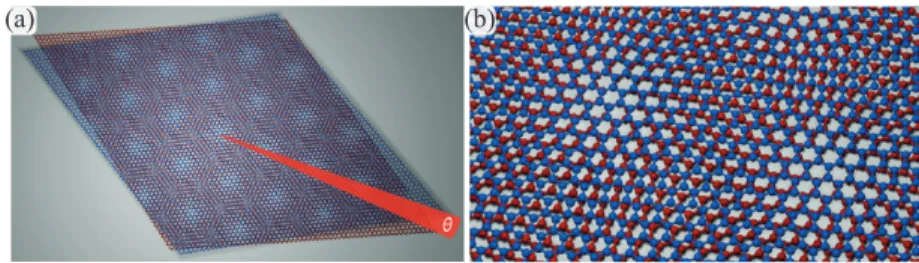
Figure 1.1: Illustration of a moiré pattern. (a) Stacking two identical honeycomb lattices (blue on top of red) with small twist angle, here𝜃=5◦. (b) Zoom-in to illustrate the atomic stacking in different regions of the moiré pattern.
pending graphene. But this was challenging in fabrication, lead to delicate devices, and introduced strain fields that modify the properties of graphene. Finally, in 2010, a big leap forward in device quality was achieved by transferring graphene from the commonly used SiO2insulating substrate to hexagonal Boron Nitride (hBN) [13, 14]. The latter is a layered, insulating material with each layer structurally nearly identical to graphene, and held together by the same van der Waals interlayer forces.
This allows to stack the two materials with little to no disorder related to structural frustration, and gets rid of impurities at the same time, resulting in much cleaner graphene devices.
The fabrication of such g/hBN devices had an unintended but remarkable conse- quence: when graphene and hBN are nearly rotationally-aligned, a structural beating pattern can be observed — amoiré pattern, seeFig. 1.1. At small twist angles, this pattern has a large (nearly-)periodic length intermediate between atomic and meso- scopic scales [13–18], i.e., 10-100 times the original lattice constant. One of the first observed consequences of the large periodic length scale was that applying a per- pendicular magnetic field leads to sizable magnetic fluxes per moiré unit cell. This allowed for the first experimental observation of Hofstadter spectra [19,20] in solid state devices, i.e., fractal magnetic subband splitting in the presence of a periodic po- tential. As we will see in more detail in this thesis, the moiré superstructure exhibits additional important implications as it effectively acts as weak periodic potential that induces elastic scattering, and profoundly affects the original low-energy band dis- persion by rearranging the spectrum into minibands [21–24]. This rearrangement is strongest near recoil energies of the periodic potential, where the hBN substrate can lead to band inversions and minigaps. Crucial to this work, it also naturally raises the question if the moiré structure can turn graphene into a valley topological insulator [TW1].
In recent years, an increasing number of two-dimensional crystals were identified besides graphene and hBN, and classified into a wider family ofvan der Waals mate- rials[25,26]. These materials cover a wide range of properties [TW1,27–29], such as
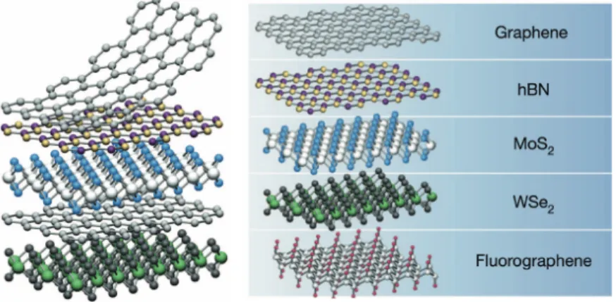
Figure 1.2: Illustration for van der Waals materials. (a) A van der Waals heterostructure stacked from individual layers of two-dimensional materials. (b) Some examples of two- dimensional materials, including graphene and hexagonal boron nitride. Reprinted from Ref. [25] with permission from Springer.
strong spin–orbit effects in transition metal dichalcogenides (TMDCs), or magnetic insulators such as CrI3. As the name suggests, these materials are characterized by strong planar bonds and weak out-of-plane van der Waals interaction, such that they can be extracted through mechanical exfoliation from bulk crystals, similar as graphene. The extracted layers can then be reassembled into a so-called van der Waals heterostructure by stacking them back together, seeFig. 1.2. Thus, there is both control over chemical composition (e.g., graphene versus hBN), as well as over geometric properties of the stack (e.g., twist-induced moiré structures).
1.3 Flat bands in twisted bilayer graphene
Studying high-quality graphene bilayers (either suspended or again on hBN sub- strates) is a natural extension of g/hBN and provides new possibilities, because the electronic properties are now also sensitive to the local stacking registry and to in- terlayer electric fields when top/bottom gates are present [30]. Like in g/hBN, twist- ing between the two graphene layers introduces a moiré superstructure and thereby alters the band dispersion by rearranging it into minibands. In contrast to g/hBN, however, interlayer coupling in twisted bilayer graphene hybridizes Dirac cones of bothlayers, which leads to a richer miniband structure. Remarkably, at fine-tuned (so-called “magic”) twist angles, the interlayer hybridization results in flat minibands at charge neutrality [18].
When the bandwidth of a flat band is on the order of Coulomb interactions or
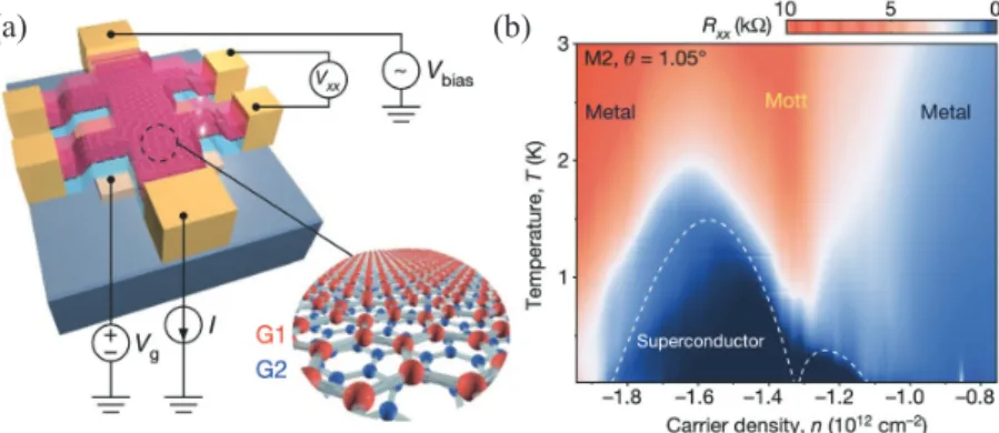
(a) (b)
Figure 1.3:First experiment demonstrating flat-band superconductivity in twisted bilayer graphene. (a) Sketch of a four-probe measurement device. The carrier density is tuned by a bottom gate. (b) Phase diagram in the four-probe resistance𝑅𝑥𝑥as a function of carrier density𝑛and temperature𝑇, showing superconducting and correlated-insulating phases.
Reprinted from Ref. [28] with permission from Springer.
smaller, the electron–electron scattering can induce strong correlations and sponta- neous symmetry breaking in the ground state, e.g., correlated insulators, magnets, charge density waves, and even superconductivity. Indeed, a correlated insulating phase was recently demonstrated in twisted bilayer graphene at the magic-angle (𝜃 ≈1.1◦) [28] and was found to transition into a unconventional superconducting state upon doping shortly after [28,31,32], see Fig1.3. This discovery launched a new wave of experimental and theoretical research into geometrically tunable flat bands with exotic correlated ground states [27,33–36]. The goal of this research is to better understand the nature of the exotic correlations, as well as to identify more regimes and other twisted multilayers (such as twisted double bilayer graphene) that feature similar flat-band correlations. In this work, we contribute to that activity by studying magnetism and valley correlations in flat-band twisted bilayer graphene.
1.4 Outline
Let us give a brief overview on the intents and contents of this work for the reader’s orientation. The chapters are grouped into three parts: introduction, background and twisted-layer systems. Theintroduction(Chapter 1) is meant to establish the historical context (as seen by the author) in which this research is embedded. The backgroundpart (Chapters 2and3) intends to provide a summary on basic con- cepts, methods, and notations relevant to understand twisted-layer graphene sys- tems. Readers who are familiar with the topic may skip over or selectively skim through it, and use it as look-up reference for the main part. The main part is de-
voted totwisted-layer systems, which presents results for three particular cases:
G/hBN In Chapter 4, we study the effective model that describes the electronic bands of graphene in presence of a hBN-induced moiré pattern, in particular in view of band topology. This low-energy continuum model describes nearly-free electronic modes with Dirac-like dispersion moving in a static, moiré-periodic effective poten- tial with threefold rotational symmetry. We find and classify the symmetry-allowed parameters of the effective potential according to how they transform under time and space inversion, and by how they rearrange the Dirac cones into minibands upon elastic scattering on the periodic potential. In this context, we study the band split- ting and the band topology of a threefold-degenerate high-symmetry point. We find that for specific parameter ranges, a band gap with non-trivial (valley) topology can be achieved at the recoil energy. We also highlight the variety of graphene or syn- thetic graphene systems, besides graphene/hBN, that may show the effective physics discussed in this chapter.
Twisted bilayer graphene (TBG) InChapter 5, we turn our attention towards flat bands in twisted bilayers (away from the magic angle) and present a mean-field anal- ysis of correlations induced by Coulomb interactions. At a twist angle of𝜃∗≈0.8◦, we find flat bands with moiré orbitals forming a triangular superlattice. Doping with
±6electrons per moiré unit cell leads to half-filling of these bands such that electronic interactions cause a Stoner instability with spin-polarized regions that order ferro- magnetically. Applying an interlayer electric field breaks inversion symmetry, and thereby induces effective Berry flux for the low-energy states that explains how the corresponding low-energy bands are modified. The electrically-induced Berry flux in- troduces valley-dependent dispersion that quenches the magnetic order. With these results, we propose a solid-state platform that realizes electrically-tunable strong cor- relations.
Magnetically encapsulated TBG InChapter 6, we continue investigating flat-band correlations, but show that they can be enforced in the valley sector by suitably hy- bridizing the spin degree of freedom through proximity to ferromagnetic insulators, such as CrI3. The interplay between twist, exchange proximity, and spin-orbit cou- pling leads to nearly valley-degenerate flat electronic bands with states forming a triangular superlattice. At half-filling, we find that interactions induce spontaneous valley-correlations that favor spiral order. We derive a low-energy valley-Heisenberg model with symmetric and antisymmetric exchange couplings. We also show how electric interlayer bias lifts the valley degeneracy and tunes these couplings.
Background
7
2
Graphene
The two-dimensional honeycomb lattice is the basic building block for many lay- ered van der Waals materials [25,26], and is of central importance to this work.
Here, we introduce its structure in real and reciprocal space, discuss simple tight- binding models defined on it, find the resulting Bloch Hamiltonians and band struc- tures, as well as derive low-energy approximations. We will discuss the monolayer case and bilayers, before we move on to twisted bilayers in the next chapter.
For more details, see contemporary reviews, e.g. Refs. [6,37].
y 1
2
A B
y
1 2 K K’
Γ M
M’
Figure 2.1: Honeycomb lattice structure in real space (left panel) and in reciprocal space (right panel). The real-space structure is characterized by lattice vectors𝒂1,2(red arrows) and sublattice atoms A (green), B (gray). Shown are also nearest-neighbor connecting lines. The reciprocal lattice is characterized by the lattice vectors𝒃1,2(gray arrows) and the hexagonal first Brillouin zone (shaded red). Shown are also high-symmetry pointsΓ, K, K’, M and M’, as well as a high-symmetry path M’→Γ→K→K’→M (blue arrows).
9
2.1 Honeycomb lattice
Let us consider a monolayer solid whose atomic constituents are arranged in a pe- riodic honeycomb lattice, seeFig. 2.1(left). The honeycomb lattice is a triangular Bravais lattice with two atoms A and B per unit cell. Each discrete unit cell position 𝒓is uniquely specified with integers𝑖, 𝑗, i.e.,
𝒓≡𝒓𝑖 𝑗 =𝑖𝒂1+𝑗𝒂2, (2.1)
with Bravais lattice vectors 𝒂1,2=𝑎
cos(𝜋/6)
±sin(𝜋/6)
= 𝑎 2
√3
±1
. (2.2)
Each atomic position is then specified by the coordinate𝒓 of the unit cell and the relative position𝒓𝛼within that unit cell, labeled by the orbital index𝛼. In our case, this is the sublattice index𝛼∈ {A,B}with orbital positions
𝒓𝐴=0, 𝒓𝐵=1/3𝒂1+1/3𝒂2=𝑎0
1 0
, (2.3)
where𝑎0 = 𝑎/√
3is the inter-atom distance. In case of graphene, we have𝑎0 ' 1.41Å, and both sublattices are occupied by carbon atoms.
We will see later that describing electronic properties of periodic crystals requires the reciprocal (dual) lattice of𝒂1,𝒂2defined through𝒂𝑖·𝒃𝑗 =2𝜋𝛿𝑖 𝑗. For the honeycomb lattice, the resulting reciprocal lattice vectors are
𝒃1,2=𝑏
cos(2𝜋/6)
±sin(2𝜋/6)
= 4𝜋
√3𝑎
cos(2𝜋/6)
±sin(2𝜋/6)
= 2𝜋
√3𝑎 1
±√ 3
. (2.4)
The primitive unit cell of the reciprocal lattice is called first Brillouin zone and can be chosen to be hexagonal in our case, as shown inFig. 2.1(right), with high-symmetry pointsΓ, M, M’, K and K’ that can be connected along a high-symmetry path.
We can now consider honeycomb bilayers, which are stacks of two identical hon- eycomb layers (𝑙=1,2) along the third dimension, seeFig. 2.2. Beside the vertical displacement along the third dimension with an interlayer distance𝑑0, the layers can have a relative horizontal displacement𝜹=(𝛿𝑥, 𝛿𝑦). The special case𝜹=𝜹AA=0 is called AA stacked, whereas𝜹=AB=𝒓𝐵−𝒓𝐴is AB (BA) stacked, indicating which atoms of the two layers are aligned. The lattice vectors𝒂1and𝒂2of the bilayer are the same as for a single layer. However, we now have four atoms𝐴1,𝐵1,𝐴2and𝐵2 per unit cell, such that within each unit cell at𝒓, we have to specify the sublattice position𝒓𝛼 [cf.Eq. (2.3)] for𝛼 ∈ {𝐴, 𝐵}, as well as the origins𝒓𝑙 of layer𝑙 =1and 𝑙=2, i.e.,
𝒓𝑙=1=0, 𝒓𝑙=2=𝜹+𝑑0ˆ𝑧. (2.5) For graphene, we have an interlayer distance of𝑑0'2.4𝑎0.
𝑥
𝑦 𝒂1
𝒂2
𝜹AA=(0,0)
𝑥
𝑦 𝒂1
𝒂2
𝜹AB=(𝑎0,0)
Figure 2.2: AA and AB stacking of two honeycomb lattices [cf.Fig. 2.1] with relative displacement𝜹=𝜹AA(left panel) and𝜹=𝜹AB(right panel) [cf.Eq. (2.5)]. Shown are the real-space lattice vectors𝒂1,𝒂2, the atoms A1 (light green), B1 (green) of the top layer, and the atoms A2 (purple), B2 (light purple) of the bottom layer. For AA stacking, all atoms of the bottom layer (purple) are covered by atoms of the top layer (green), and for AB stacking, all B2 atoms lie on top of A1 atoms.
2.2 Tight‐binding model and band structures
In theatomic limit, we describe each isolated atom through electronic orbitals with discrete energy levels. The latter are then filled by electrons until the overall atom is charge neutral. In a solid, proximity to neighboring atoms leads to overlap and hybridization of the outermost electronic orbitals, which in turn leads to extended states and broadening of the corresponding energy level into a dispersiveband.
In graphene,𝑠𝑝2hybridization is responsible for the honeycomb arrangement, such that two electrons per atom occupy the1𝑠orbital, and three electrons per atom par- ticipate in a strong bond to nearest neighbors (hybridized𝑠,𝑝𝑥and𝑝𝑦orbitals) and one valence electron occupies the𝑝𝑧orbital. It suffices to focus on this valence elec- tron, which we describe with a tight-binding Hamiltonian in second quantization as
𝐻0= X
(𝑖,𝛼)≠(𝑗,𝛽)
𝑡𝛼𝛽(𝒓𝑖−𝒓𝑗)𝑐𝑖𝛼†𝑐𝑗𝛽+X
𝑖,𝛼𝑉𝛼(𝒓𝑖)𝑐†𝑖𝛼𝑐𝑖𝛼, (2.6a) where𝑐𝑖𝛼(†) destroys (creates) an electron in orbital𝛼of the unit cell centered at po- sition𝒓𝑖. Here, the sublattice𝛼∈ {A,B}is the only orbital degree of freedom taken into account. The hopping amplitude between two orbitals𝛼and𝛽in cells𝑖and𝑗, re- spectively, is𝑡𝛼𝛽(𝒓𝑖−𝒓𝑗)and𝑉𝛼(𝒓)is the local potential. As we will see in chapter3, the overlap𝑡𝛼𝛽(𝒓𝑖−𝒓𝑗) =𝑡(𝒓𝑖+𝒓𝛼−𝒓𝑗−𝒓𝛽)decays exponentially with distance.
The hopping amplitudes are then dominant between nearest neighbors (i.e., A and B sites) in the same or in neighboring unit cells shifted by lattice vectors𝑹, i.e.,
𝑡𝐴𝐵(𝑹)=−𝑡, for 𝑹∈ {0,𝒂1,𝒂2}, (2.6b)
and we have𝑡𝐵𝐴(−𝑹)=𝑡𝐴𝐵(𝑹)∗due to self-adjointness of𝐻0. If the atoms A and B are not of the same type, we have to account for a sublattice imbalance via
𝑉𝐴(𝒓)=Δ, 𝑉𝐵(𝒓)=−Δ. (2.6c)
For graphene, all sites are occupied by carbon atoms such that there is no sublattice imbalance, i.e.,Δ= 0. In contrast, the hexagonal boron nitride (hBN), which has a nearly identical crystal structure, has two different atoms boron (B) and nitrogen (N) on the respective sublattice, leading to a significant difference in local chemical potential such thatΔ>0.
We can write the periodic Hamiltonian (2.6a) in the general form 𝐻0=X
𝒓,𝑹Ψ𝒓+𝑹† ℎ𝑹Ψ𝒓, (2.7)
where𝒓,𝑹∈ {𝑖𝒂1+𝑗𝒂2|𝑖, 𝑗∈ℕ}are unit cell positions, we introducedΨ𝒓𝑖 =(𝑐𝑖𝐴, 𝑐𝑖𝐵) as unit cell operators, and(ℎ𝑹)𝛼𝛽are2×2matrices containing the hopping ampli- tudes between sublattice𝛽at𝒓and𝛼at𝒓+𝑹. We can exploit the discrete translational symmetries by using the Fourier operator basis
Ψ(𝒌)= 1
√𝑁 X
𝒓 𝑒−𝑖𝒌·𝒓 Ψ𝒓, (2.8)
where𝑁 1is the number of unit cells in the sample. In this basis, we find 𝐻0= X
𝒌∈BZ
Ψ(𝒌)†ℎ(𝒌)Ψ(𝒌), with ℎ(𝒌)=X
𝑹 𝑒𝑖𝒌·𝑹ℎ𝑹, (2.9) whereℎ(𝒌)is the so-calledBlochHamiltonian, which satisfiesℎ(𝒌+𝑖𝒃1+𝑗𝒃2)=ℎ(𝒌) for integers𝑖, 𝑗, i.e., periodicity in reciprocal space. Hence, we can restrict ourselves to the first Brillouin zone, i.e.,𝒌∈BZ. We diagonalize the Bloch Hamiltonianℎ(𝒌) to find the single-particle eigenvalues𝜀𝑛(𝒌) and eigenvectors|𝜓𝑛(𝒌)i, where the integer𝑛is the band index.
In our case, with Eqs. (2.6), the Bloch Hamiltonian (2.9) is ℎ(𝒌)=
Δ −𝑡(1+𝑒𝑖𝒌·𝒂1+𝑒𝑖𝒌·𝒂2)
−𝑡(1+𝑒−𝑖𝒌·𝒂1+𝑒−𝑖𝒌·𝒂2) −Δ
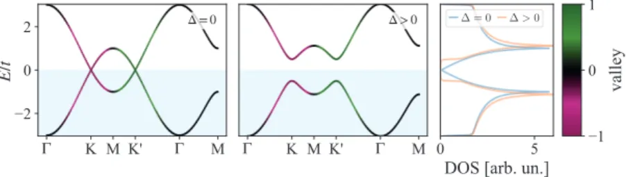
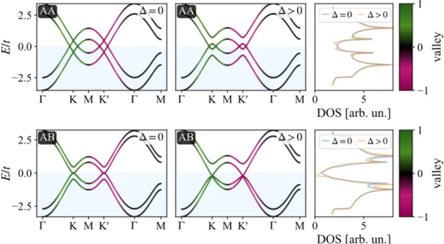
, (2.10) and the resulting band structure𝜀𝑛(𝒌)along a high-symmetry path in the first Bril- louin zone and the density of states is shown inFig. 2.3, for the casesΔ= 0(e.g., graphene) andΔ > 0(e.g., hBN case). Interestingly, we see that graphene is a semimetal at charge neutrality due a band touching in each valley K and K’. In con- trast, for finite sublattice imbalance, a direct band gap opens up at the valleys.
∆ = 0 ∆>0
Figure 2.3: Electronic spectrum of a monolayer honeycomb lattice model. Shown are band structures (first two panels) and density of states (last panel) for nearest-neighbor tight-binding hopping, seeEq. (2.10)with hopping amplitudes𝑡 =2.7eV and sublattice imbalancesΔ=0andΔ=0.5𝑡. The most striking features are the so-calledDirac cones atvalleys𝐾and𝐾0showing up in graphene (Δ=0). Finite sublattice imbalance (Δ>0) breaks inversion symmetry and opens a bandgap, as is the case for hexagonal boron nitride (hBN). The density of states (DOS) is given by𝜌(𝐸)=P
𝑛,𝒌𝛿(𝐸−𝜀𝑛(𝒌)), summing over bands𝑛and Bloch momenta𝒌. Even forΔ=0, the density of states vanishes at the band touching (𝐸=0). The band colors (purple to green) are expectation values of the valley operator𝑣𝑧(see AppendixA.1), i.e.,h𝜓𝑛(𝒌) |𝑣𝑧|𝜓𝑛(𝒌) ifor Bloch states|𝜓𝑛(𝒌) i.
In the simple case ofEq. (2.10), the Bloch bands can be found explicitly, i.e., 𝜀𝑛(𝒌)=𝑠𝑛
vu t
Δ2+𝑡2 3+ X
𝑗=0,...,5cos
𝒌·𝑅2𝜋/6𝑗𝒂1
!, (2.11)
with𝑠1=−1and𝑠2=1, and𝑅𝜙 ∈SO(2)is a rotation by an angle𝜙.
The discussion for monolayer graphene can readily be generalized to bilayer graphene (BLG), where we now have both a sublattice index𝛼 ∈ {𝐴, 𝐵}and the layer index𝑙=1,2as orbital labels. For AA-bilayer graphene, we then find the4×4 Bloch Hamiltonian
ℎAA-BLG(𝒌)=
ℎ(𝒌) 𝑡⊥12
𝑡⊥12 ℎ(𝒌)
, (2.12)
whereℎ(𝒌) is the Bloch Hamiltonian (2.10) of a single layer and𝑡⊥is the nearest- neighbor interlayer hopping amplitude; for graphene typically𝑡⊥'0.15𝑡. For AB- bilayer graphene and BA-bilayer graphene, the Bloch Hamiltonian is
ℎAB-BLG(𝒌)=
ℎ(𝒌) 𝑡⊥
0 0
𝑡⊥ ℎ(𝒌)
, ℎBA-BLG(𝒌)=
ℎ(𝒌) 0
𝑡⊥ 𝑡⊥
0 ℎ(𝒌)
. (2.13)
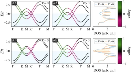
InFig. 2.4, we show the band structures along a high-symmetry path in the Brillouin zone and the densities of states for the bilayer models (2.12) and (2.13). We see that in
Figure 2.4:Electronic spectrum of AA and AB bilayers of two identical honeycomb lattices [cf.Fig. 2.2], with and without sublattice imbalanceΔ. Shown are band structures and density of states [cf.Fig. 2.3] for nearest-neighbor tight-binding models (2.12) and (2.13), with hopping amplitude𝑡=2.7eV and sublattice imbalancesΔ=0andΔ=0.5𝑡. In AA bilayer graphene (Δ=0), the low-energy bands are given by Dirac cones that are displaced in energy, see alsoFig. 2.7. Interestingly, for AB bilayer graphene (Δ=0) each valley𝐾 and𝐾0features aquadraticband touching, cf.Fig. 2.7. Note that for both stackings, bilayer graphene has a finite density of states at𝐸=0. Band colors are expectation values of the valley operator𝑣𝑧(see AppendixA.1) as inFig. 2.3.
particular the low-energy band structure near𝐸=0greatly differs between AA and AB stacking. The former is highly dispersive, while the latter features a quadratic band touching.
Interestingly, bilayers offer one more tunable knob compared to single layers: one can apply an electric bias𝑉 between the two layers (in practice achieved with top and bottom gates), which translates into different chemical potentials for each layer, i.e.,
ℎ𝑋-BLG(𝒌) ↦→ ℎ𝑋-BLG(𝒌) +𝑉 2
12
−12,
(2.14) where𝑋 =AA,AB,BAdenotes the stacking. InFig. 2.5, we again show the band structures along the high-symmetry path in the Brillouin zone and densities of states for the bilayer models (2.12) and (2.13), while including interlayer bias𝑉 as inEq. (2.14). Whereas the electronic bands of AA bilayer graphene are mostly unaffected, for the AB bilayer, the interlayer bias induces a band gap and opens the quadratic band touching at the valleys.
Figure 2.5: Electronic spectrum of a AA and AB bilayer of two identical honeycomb lat- tices [cf.Fig. 2.2] with interlayer bias𝑉 (butwithoutsublattice imbalance, cf.Fig. 2.4), seeEq. (2.14). Shown are band structures and density of states [cf.Fig. 2.3] for a nearest- neighbor tight-binding model (2.12) and (2.13), with hopping amplitude𝑡 = 2.7eV and interlayer bias𝑉=0and𝑉=0.8𝑡. In AB bilayer graphene, the quadratic band touchings in valleys𝐾and𝐾0get gapped out by finite interlayer bias𝑉>0. Band colors are expec- tation values of the valley operator𝑣𝑧(see AppendixA.1) as inFig. 2.3.
2.3 Low‐energy continuum approximation
Many physical properties of a solid are dominated by the states near the chemical potential. Consequently, it is often sufficient to know the low-energy band disper- sion, e.g., from𝒌·𝒑perturbation theory. For monolayer graphene, we saw that the low-energy bands near half-filling (𝐸 = 0) are located in the valleys K and K’, and have a band touching with linear dispersion, seeFigs. 2.3and2.6. Expanding the Hamiltonian (2.10) near these valleys then results in aDirac-likeHamiltonian
ℎ𝜉(𝒒) ≡ℎ(𝜉𝑲+𝒒)= ℏ𝑣𝐹𝒒·𝝈𝜉+Δ𝜎3+𝑂(𝑞2), (2.15) where𝜉 = ±selects the valley, 𝑣𝐹 = (3/2)𝑎𝑡/ℏis the Fermi velocity (for lattice constant𝑎) and𝝈±=(±𝜎1, 𝜎2)is the vector operator with Pauli matrices
𝜎0= 1 0
0 1
, 𝜎1= 0 1
1 0
, 𝜎2= 0 −𝑖
𝑖 0
, 𝜎3= 1 0
0 −1
. (2.16) The Hamiltonianℎ𝜉(𝒒)is called Dirac-like, because similar to the description of elec- trons in high-energy physics, the energy momentum relation is linear at higher en- ergies, and has particle/hole branches. Grouping both Dirac-like Hamiltonians in a
(a) (b)
Figure 2.6:Band structure of the monolayer honeycomb lattice with nearest-neighbor hop- ping amplitudes [cf.Fig. 2.3], highlighting the Dirac cones. (a) Bands on the first Brillouin zone [cf.Fig. 2.1] for the case of graphene (Δ=0) such that cones at the high-symmetry points K, K’ are prominent. (b) Zoom-in on the Dirac cone at K [see dotted circle in (a)], with linear dispersion highlighted, and with a finite sublattice imbalanceΔ> 0to illus- trate the opening of a band gap in the cone.
Block basis
𝑇(𝒒)= ℎ+(𝒒)
ℎ−(𝒒)
, (2.17)
for graphene (Δ=0), the Hamiltonian is formally equivalent to the Weyl Hamilto- nian of high-energy physics. The sublattice imbalanceΔgaps the Dirac-like cones, and induces a finitemassfor the band electron, seeFig. 2.6(b), and is hence often referred to as Dirac massΔ.
The low-energy expansion is also known as continuum approximation, because what we effectively did in this chapter, was to write the Hamiltonian in a modulated plane- wave basis (Bloch basis), and to factor out the envelope function that varies on a long scale compared to the lattice constant𝑎, i.e.,
𝜓(𝒙)=𝑒𝑖𝑲·𝒙 X
𝑞2𝜋/𝑎𝑒𝑖𝒒·𝒙𝜓+(𝒒) +𝑒−𝑖𝑲·𝒙 X
𝑞2𝜋/𝑎𝑒𝑖𝒒·𝒙𝜓−(𝒒), where𝜓𝜉(𝒒)are eigenfunctions of the continuum Hamiltonianℎ𝜉(𝒒).
Note that it is common to rewrite the continuum Hamiltonian (2.17) by applying the basis transform
𝑈 = 1 0
0 𝜎2
(2.18) to find
𝑇˜(𝒒)=𝑈†𝑇(𝒒)𝑈=𝑣𝐹ℏ𝒒·𝝈𝜏0+Δ𝜎3𝜏3, (2.19)
(a)AA (b) AB
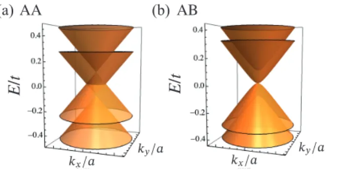
Figure 2.7:Low-energy bands in valley𝐾of the AA and AB honeycomb bilayer [cf.Fig. 2.5]
with nearest-neighbor tight-binding hopping amplitudes, and interlayer coupling𝑡⊥ ' 0.1𝑡[cf. Eqs. (2.12)and(2.13)]. (a) In case of AA stacking, we find two Dirac cones per valley, split in energy by interlayer hybridization𝑡⊥, and (b) in case of AB stacking, the low-energy bands feature a quadratic band touching, with parabolic bands split away by interlayer hybridization𝑡⊥.
where𝜏𝑗are again the Pauli matrices, but now for the valley degree of freedom.1In this form, the linear contribution in both valleys takes the same form. In this basis, One can show that the action of spatial inversion is given byI = 𝜏2𝜎3 and time- reversal is given by the antiunitary operatorT=𝜏1𝜎2K, whereKdenotes complex conjugation.
The previous discussion of the low-energy approximation naturally applies also to the Hamiltonians inEqs. (2.12)and(2.13)for AB and BA bilayer graphene. The de- grees of freedom per valley are then doubled due to the addition of a layer coordinate.
The low-energy model then features4bands per valley, as shown inFig. 2.7.
2.4 Topological aspects
The study of topological effects in condensed matter has become an important and flourishing field, as attested for by a Nobel prize awarded to David J. Thouless, F. Dun- can M. Haldane, and J. Michael Kosterlitz in 2016 for their various contributions [8, 38–41]. Topology in the spaces of Hamiltonian operators has various remarkable consequences, such as edge modes in finite samples and robustly quantized trans- port even in the presence of significant disorder, such as is the case for the Quantum Hall Effect (QHE). Instead of delving into an exhaustive overview, we summarize the basic concepts needed for this work. More details and derivations can be found in Refs. [37,42].
1New symbols for the same Pauli matrices allow to avoid writing tensor products:𝜎𝑖𝜏𝑗=𝜏𝑗𝜎𝑖=𝜎𝑖⊗ 𝜎𝑗≠𝜎𝑗⊗𝜎𝑖.
2.4.1 Berry curvature in the dynamics of band electrons
Consider a Hamiltonianℎ(𝒌)that depends on some parameters𝒌(in our case crystal momentum in the first Brillouin zone) and has eigensolutions
ℎ(𝒌) |𝑢𝑛(𝒌)i=𝜀𝑛(𝒌) |𝑢𝑛(𝒌)i. (2.20) If we vary the parameters𝒌≡𝒌(𝑡)adiabatically in time𝑡, we can use the adiabatic theorem to find that the initial state|𝑢𝑛(𝒌(0))ievolves into instantaneous eigen- states|𝑢𝑛(𝑡)iwith a dynamical phase, i.e.,
|𝑢𝑛(𝑡)i=exp
𝑖 𝛾𝑛(𝑡) −𝑖 ℏ
∫𝑡
0𝜀𝑛(𝒌(𝑡0))d𝑡
|𝑢𝑛(𝒌(𝑡))i, (2.21) with the additionalBerry phase
𝛾𝑛=
∫
CA𝑛(𝒌) ·d𝒌, (2.22)
whereCis the trajectory of𝒌and we defined the so-calledBerry connection A𝑛(𝒌)=𝑖 h𝑢𝑛(𝒌)|∇𝑘|𝑢𝑛(𝒌)i. (2.23) While the connection A𝑛(𝒌) changes under gauge transformations |𝑢˜𝑛(𝒌)i = 𝑒𝑖𝜙(𝒌)|𝑢𝑛(𝒌)i, it turns out that for closed pathsC=𝜕𝑆the phase𝛾𝑛becomes gauge independent, i.e.,
𝛾𝑛=1 2
∫
𝑆Ω𝑛𝑖 𝑗(𝒌) d𝑘𝑖∧d𝑘𝑗 (2.24) with implied summation over repeated indices, and exterior productd𝑘𝑖 ∧d𝑘𝑗 as differential area element. To obtainEq. (2.24), we used Stokes’s theorem2and defined theBerry curvature
Ω𝑛𝑖 𝑗(𝒌)=𝜕𝑖A𝑛𝑗(𝒌) −𝜕𝑗A𝑛𝑖(𝒌)=𝑖
h𝜕𝑖𝑢𝑛(𝒌)|𝜕𝑗𝑢𝑛(𝒌)i − (𝑖↔𝑗)
, (2.25) where in the last step we inserted the Berry connection (2.23) and used the notation
𝜕/𝜕𝑘𝑖 ≡𝜕𝑖. We can remove the derivatives from the states to obtain a useful formula3 Ω𝑛𝑖 𝑗(𝒌)=𝑖X
𝑛0≠𝑛
h𝑢𝑛|𝜕𝑖ℎ|𝑢𝑛0i h𝑢𝑛0|𝜕𝑗ℎ|𝑢𝑛i − (𝑖↔𝑗)
(𝜀𝑛−𝜀𝑛0)2 , (2.26)
2Stokes’ theorem:∫
𝜕𝑉𝜔=∫
𝑉d𝜔for a differential form𝜔over the boundary of a manifold𝑉, and the exterior derivatived𝜔. In our case, we have the1-form𝜔=P
𝑖A𝑖d𝑘𝑖such thatd𝜔=P
𝑖 𝑗𝜖𝑖 𝑗𝜕𝑖A𝑗d𝑘𝑖∧ d𝑘𝑗with exterior product∧.
3Let us briefly sketch the derivation: First, we insert the resolution to the identity1 = |𝑢𝑛ih𝑢𝑛| + P𝑛0≠𝑛|𝑢𝑛0ih𝑢𝑛0|intoEq. (2.25). Second, we note that forℎ|𝑛i=𝜀𝑛|𝑛i, the relation h𝑛|𝜕𝑖ℎ|𝑛0i=(𝜀𝑛− 𝜀𝑛0) h𝜕𝑖𝑛|𝑛0iholds for𝑛≠𝑛0. It follows from applying the product rule to0=𝜕𝑖h𝑛|ℎ|𝑛0iand to0=
𝜕𝑖h𝑛|𝑛0i, and combining the resulting equations. Equation (2.26) then follows immediately.
where in the last step we did not explicitly write the𝒌 dependences. The for- mula (2.26) for the Berry curvature is manifestly independent of the gauge choice for the wave functions, which makes it useful for numerical computations (see appendixBfor an even more useful formulation). If the parameter space is two- dimensional, i.e.,𝒌=(𝑘𝑥, 𝑘𝑦), we can calculate the Berry phase (2.24) as
𝛾𝑛=
∫
𝑆Ω𝑛𝑥𝑦(𝒌)d2𝑘 . (2.27)
We will often be interested in integrating over the Brillouin zone,𝑆=BZ. In partic- ular in1D, this Berry phase is also known as Zak’s phase.
We now saw that the Berry curvatureΩ𝑛𝑖 𝑗(𝒌)enters the time-evolution of the wave- functions. To understand this point better, we can study the dynamics of a Gaussian wave packet with mean position𝒓(𝑡) and central wave vector𝒌(𝑡) in an external electric field𝑬and magnetic field𝑩. It can be shown that such wave packets follow the semi-classical equations of motion [37]
¤
𝒓= ℏ−1∇𝑘𝜀𝑀(𝒌) − ¤𝒌×𝛀(𝒌) (2.28a)
ℏ𝒌¤ =−𝑒𝑬−𝑒𝒓¤×𝑩, (2.28b)
where𝜀𝑀(𝒌) = 𝜀(𝒌) −𝑩×𝒎(𝒌) is the band dispersion modified by the orbital magnetic moment𝒎of the wave packet4and we used the vector form𝛀for the Berry curvature given byΩ𝑖 𝑗 =𝜖𝑖 𝑗𝑚(𝛀)𝑚with Levi-Civita tensor𝜖𝑖 𝑗𝑚. Interestingly, we see that due to the formal similarity between the two equations, the Berry curvature 𝛀can be interpreted as an effective magnetic field in reciprocal space. Both𝛀and 𝑩have the tendency to induce transverse responses in the wave packet dynamics. It can be shown [37] that in case of time reversal symmetry the curvature𝛀(𝒌)must be even, and that in case of inversion symmetry it must be odd. If both symmetries are present, we thus have𝛀(𝒌)=0for all𝒌.
Remarkably, linear response theory (Kubo formula) relates the the Berry curvature to the transverse conductance of a two-dimensional band insulator with [37]
𝜎𝑥𝑦=𝑒2 ℏ
X
𝑛
∫
BZΩ𝑛𝑥𝑦(𝒌) d2𝑘 (2𝜋)2 =𝑒2
ℎ X
𝑛 𝐶𝑛, (2.29)
where we sum over fully occupied bands𝑛. We introduced theChern number𝐶𝑛= 𝛾𝑛/(2𝜋), which for closed manifolds (such as the Brillouin zone) characterizes the map from the parameter space𝒌to the Bloch states|𝑢𝑛(𝒌)i, and must be quantized (𝐶𝑛 ∈ ℕ) due to the requirement that the wavefunction is single-valued. The re- markable quantization inEq. (2.29)is realized in the Quantum Hall Effect, where increasing the magnetic field strength𝐵sweeps the chemical potential over various Landau bands that are separated by insulating gaps. The robustness of the quantized
4See Ref. [37] for details.
Hall response in presence of disorder crucially relies ontopology: It turns out that all smooth deformations of the Hamiltonian which leave the band gap intact, have the same integer topological index – in our case the Chern numberP
𝑛𝐶𝑛. Conse- quently, only perturbations that induce band inversions between two or more bands can possibly change the Chern number and the Hall response𝜎𝑥𝑦. Note that the latter observation is the basis for modern topological physics: Hamiltonians are grouped according to equivalence classes induced by smooth deformations which leave the band gaps intact, and sometimes those which additionally preserve structural sym- metries of periodic crystals.
2.4.2 Trivial and topological bands in monolayer graphene
We found inSections 2.2and2.3that monolayer graphene has two bands that cross with a Dirac-like linear dispersion near the valleys K and K’, i.e., it does not have a spectral gap. However, inSection 2.4.1, we saw that spectral gaps are crucial to be able to talk about band topology. Hence, we now explore different ways of inducing a spectral gap in monolayer graphene and compute the Berry curvature and Chern number. To this end, we discuss the Haldane model [8] on the honeycomb lattice.
Let us go back to Hamiltonian (2.6) for monolayer graphene, but this time include both a possible sublattice imbalanceΔand also thenext-nearest neighbor hopping amplitude𝑡0. The latter can acquire a Peierls phase𝜙 in presence of magnetic flux [43], which we here choose to be induced by a staggered magnetic field5as depicted inFig. 2.8(a). For this magnetic flux pattern, the new hopping amplitudes are
𝑡𝐴𝐴(𝑹)=𝑡𝐵𝐵(𝑹)∗=𝑡0𝑒𝑖𝜙, 𝑡(−𝑹)=𝑡(𝑹)†, (2.30) for𝑹 ∈ n
𝒂1, 𝑅2𝜋/3𝒂1, 𝑅22𝜋/3𝒂1
o, where𝑅𝜃 ∈ SO(2) is again a rotation by angle𝜃.
The corresponding Bloch Hamiltonian [cf.Eq. (2.10)] then is ℎ(𝒌)=
Δ0(𝒌) +Δ00(𝒌) +Δ −𝑡(1+𝑒𝑖𝒌·𝒂1+𝑒𝑖𝒌·𝒂2)
−𝑡(1+𝑒−𝑖𝒌·𝒂1+𝑒−𝑖𝒌·𝒂2) Δ0(𝒌) −Δ00(𝒌) −Δ
, (2.31)
where
Δ0(𝒌)=2𝑡0cos(𝜙) X2
𝑗=0cos
𝑅2𝑗𝜋/3𝒂1·𝒌
, Δ00(𝒌)=2𝑡0sin(𝜙) X2
𝑗=0sin
𝑅2𝑗𝜋/3𝒂1·𝒌 .
We can once more expandℎ(𝒌)at low energies around valleys K and K’ and find the effective Dirac-like Hamiltonian for both valleys [cf. Eq. (2.19)]
𝑇˜(𝒒)=𝑣𝐹ℏ𝒒·𝝈𝜏0+ (Δ𝜏3+ΔH𝜏0)𝜎3, (2.32)
5Note that the flux pattern considered here has net zero flux per unit cell and preserves all structural symmetries, such that there is no need to introduce magnetic unit cells.
![Figure 2.2: AA and AB stacking of two honeycomb lattices [cf. Fig. 2.1] with relative displacement](https://thumb-eu.123doks.com/thumbv2/1library_info/3906653.1525629/21.629.126.501.104.278/figure-stacking-honeycomb-lattices-relative-displacement-panel-right.webp)

![1. Electronic Band Structure Within the Tight Binding Model . . . [10P]](data:image/gif;base64,R0lGODlhAQABAIAAAP///wAAACH5BAEAAAAALAAAAAABAAEAAAICRAEAOw==)