Scalable Tight-Binding Model for Graphene
Ming-Hao Liu (劉明豪),1,* Peter Rickhaus,2 Péter Makk,2Endre Tóvári,3 Romain Maurand,4 Fedor Tkatschenko,1 Markus Weiss,2 Christian Schönenberger,2 and Klaus Richter1
1Institut für Theoretische Physik, Universität Regensburg, D-93040 Regensburg, Germany
2Department of Physics, University of Basel, Klingelbergstrasse 82, CH-4056 Basel, Switzerland
3Department of Physics, Budapest University of Technology and Economics and Condensed Matter Research Group of the Hungarian Academy of Sciences, Budafoki ut 8, 1111 Budapest, Hungary
4University Grenoble Alpes and CEA-INAC-SPSMS, F-38000 Grenoble, France (Received 21 July 2014; published 22 January 2015)
Artificial graphene consisting of honeycomb lattices other than the atomic layer of carbon has been shown to exhibit electronic properties similar to real graphene. Here, we reverse the argument to show that transport properties of real graphene can be captured by simulations using“theoretical artificial graphene.” To prove this, we first derive a simple condition, along with its restrictions, to achieve band structure invariance for a scalable graphene lattice. We then present transport measurements for an ultraclean suspended single-layer graphene pn junction device, where ballistic transport features from complex Fabry-Pérot interference (at zero magnetic field) to the quantum Hall effect (at unusually low field) are observed and are well reproduced by transport simulations based on properly scaled single-particle tight- binding models. Our findings indicate that transport simulations for graphene can be efficiently performed with a strongly reduced number of atomic sites, allowing for reliable predictions for electric properties of complex graphene devices. We demonstrate the capability of the model by applying it to predict so-far unexplored gate-defined conductance quantization in single-layer graphene.
DOI:10.1103/PhysRevLett.114.036601 PACS numbers: 72.80.Vp, 72.10.−d, 73.23.Ad
Graphene is a promising material for its special electrical, optical, thermal, and mechanical properties. In particular, the conic electronic structure that mimics two-dimensional (2D) massless Dirac fermions has attracted much attention on both the academic and industrial sides. Soon after the
“debut”of single-layer graphene [1,2]and the subsequent confirmation of its relativistic nature[3–5], the exploration of Dirac fermions in condensed matter has been further extended to honeycomb lattices other than graphene, including optical lattices[6–8], semiconductor nanopattern- ing [9–12], molecular arrays on Cu(111) surfaces [13], or even macroscopic, dielectric resonators for microwave propagation [14,15], all of which have been shown to exhibit similar electronic properties as real graphene and hence are referred to asartificial graphene[16].
Here, we reverse the argument to show that transport properties of real graphene can be captured by simulations using“theoretical artificial graphene,”by which we mean a honeycomb lattice with its lattice spacingadifferent from the carbon-carbon bond length a0 of real graphene; see Fig. 1. From a theoretical point of view, this can be achieved only if the considered theoretical artificial lattice, which will be shortly referred to as artificial graphene or scaled graphene, has its energy band structure identical to that of real graphene. In this Letter, we first derive a simple condition, along with its restrictions, to achieve the band structure invariance of graphene with its bond length scaled from a0 to a, even in the presence of a magnetic field.
We then prove the argument by presenting transport
measurements for an ultraclean suspended single-layer graphene pn junction device, where ballistic transport features from Fabry-Pérot interference to the quantum Hall effect are observed and are well reproduced by quantum transport simulations based on the scaled gra- phene. To go one step further, we demonstrate the capabil- ity of the scaling approach by applying it to uncover one of the experimentally feasible yet unexplored transport regimes: gate-defined zero-field conductance quantization.
We begin our discussion with the standard tight-binding model for 2D graphite[17], i.e., bulk graphene, and focus
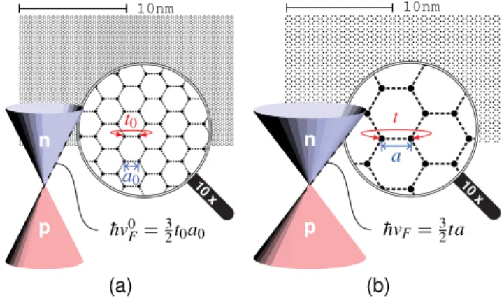
FIG. 1 (color online). Schematic of a sheet of (a) real graphene and (b) scaled graphene and their conical low-energy band structures. In (a), the lattice spacinga0≈0.142nm, the hopping energyt0≈2.8eV, and the Fermi velocityv0F≈108cm s−1.
on the low-energy range (jEj≲1eV) which is addressed in most graphene transport measurements. In this regime, the effective Dirac HamiltonianHeff ¼vFσ·passociated with the celebrated linear band structure EðkÞ ¼ ℏvFjkj describes the graphene system well. Here, vF≈108cms−1 is the Fermi velocity in graphene, and ℏk, the eigenvalue of the operatorσ·p[Pauli matricesσ¼ ðσx;σyÞact on the pseudospin properties], is the quasimomentum with k defined relative to the K orK0 point in the first Brillouin zone. In terms of the tight-binding parameters, one replaces ℏvF with ð3=2Þt0a0, where t0≈2.8eV is the nearest neighbor hopping parameter anda0≈0.142nm is the lattice site spacing, i.e.,E0ðkÞ ¼ ð3=2Þt0a0kfor real graphene[18].
Now, we consider the scaled graphene described by the same tight-binding model but with hopping parametertand lattice spacingaand introduce a scaling factorsfsuch that a¼sfa0. The real and scaled graphene sheets along with their low-energy band structures are schematically sketched in Fig. 1. The low-energy dispersion for scaled graphene is naturally expected to beEðkÞ ¼ ð3=2Þtak. Thus, to keep the energy band structure unchanged while scaling up the bond length by a factor ofsf, the condition
a¼sfa0; t¼t0
sf ð1Þ
becomes self-evident.
Clearly, Eq. (1) applies only when the linear approxi- mation is valid. In terms of the long wavelength limit, this means that the Fermi wavelength should be much longer than the lattice spacing:λF ≫a, from which using Eq.(1) the following validity criterion can be deduced:
sf≪ 3t0π
jEmaxj; ð2Þ whereEmaxis the maximal energy of interest for investigating a particular real graphene system. Considering graphene on a typical Si=300 nm SiO2 substrate, the usually accessed carrier density range is less than1013 cm−2[1]. This implies that the energy range of interest lies withinjEmaxj≲0.4eV, leading to sf ≪66from Eq.(2)(using t0¼2.8eV). For suspended graphene, typical carrier densities can hardly reach1012 cm−2[19], so thatjEmaxj≲0.1eV allows for a larger range of the scaling factorsf ≪264.
In the presence of an external magnetic field, the Peierls substitution[20]is the standard method to take into account the effect of a uniform out-of-plane magnetic field Bz within the tight-binding formulation. In addition to the long wavelength limit(2), the validity of the Peierls substitution, however, imposes a further restriction for the scaling[21]:
lB≫a, where lB¼ ffiffiffiffiffiffiffiffiffiffiffiffiffi ℏ=eBz
p is the magnetic length. In terms ofa¼sfa0 given in Eq.(1), this restriction reads
sf≪lB
a0≈p180ffiffiffiffiffiBz; ð3Þ
whereBz is in units of T. Equations(1)–(3) complete the description of band structure invariance for scaled graphene.
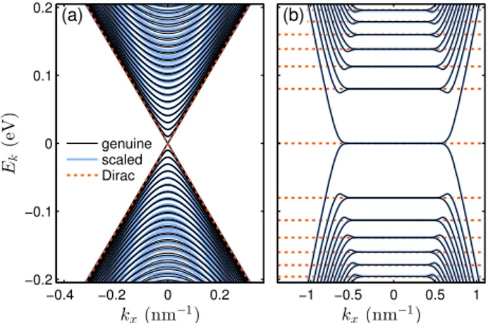
The above discussion is based on bulk graphene, but the listed conditions apply equally well to finite-width gra- phene ribbons. To show a concrete example of band structure invariance under scaling, we consider a 200- nm-wide armchair ribbon and compare the band structures of the genuine case withsf ¼1and the scaled case with sf ¼4in Fig.2(a) forBz¼0. The scaled graphene band structure well matches the genuine one at low energyjEj≲ 0.1eV and starts to deviate at higher energy but stays rather consistent within the shown energy range ofjEj≤0.2eV.
Both of the band structures are well bound by the linear Dirac model that corresponds to the bulk graphene. The band structure invariance remains true when a magnetic field is applied, as seen in Fig. 2(b), where Bz¼5T is considered. The pronounced flat bands in both cases match perfectly with the relativistic Landau levels EnL ¼sgnðnLÞ ffiffiffiffiffiffiffiffiffiffiffiffiffiffiffiffiffiffiffiffiffiffiffiffiffi
2eBzℏv2FjnLj
p solved from the Dirac
model [3–5,21], where nL¼0;1;2;…. The band structure invariance based on Eqs. (1)–(3) can be easily shown to hold also for zigzag graphene ribbons.
Having demonstrated that under proper conditions (1)–(3)the scaled graphene band structure can be identical to that of real graphene, we next perform quantum transport simulations for a real graphene device, using the scaled graphene. To this end, we have fabricated ultraclean suspended graphenepnjunctions as sketched in Fig.3(a).
First, bottom gates were prepatterned on a Si wafer with 300 nm SiO2oxide. Afterwards, the wafer was spin coated with lift-off resist, and the graphene was transferred on top following the method described in Ref. [22]. Palladium contacts to graphene were made bye-beam lithography and thermal evaporation, and the device was suspended by
FIG. 2 (color online). Band structure consistency check using an armchair graphene ribbon with width 200 nm (a) in the absence of magnetic field and (b) in the presence of a uniform magnetic fieldBz¼5T. The comparison is done for both (a) and (b) between the genuine graphene with sf¼1 and scaled graphene withsf¼4, which correspond to chain numbersNa¼ 800andNa¼200, respectively.
exposing and developing the lift-off resist. Finally, the graphene was cleaned by current annealing at 4 K. The fabrication method is described in Refs. [23,24]in detail.
Following the device design of our experiment [sketched in Fig. 3(a)], we first build a three-dimensional (3D) electrostatic model to obtain the self-partial capacitances [25,26]of the individual metal contacts and bottom gates, which are computed by the finite-element simulator FENICS [27] combined with the mesh generator GMSH [28].
The extracted self-partial capacitances from the electrostatic simulation provide us the realistic carrier density profile (see the Supplemental Material[29])nðx; yÞat any combi- nation of the left and right bottom gate voltagesVLandVR, respectively. In Fig.3(b), we plot the mean carrier densityn¯ averaged over the whole suspended graphene region as a function of Vg ¼VL¼VR. The slope reveals a charging efficiency of the connected bottom gates of about 1010 cm−2V−1, which is slightly lower than the experimen- tal value of1.24×1010 cm−2V−1extracted from the uni- polar quantum Hall data[29].
In the absence of magnetic field, the Fermi energy as a function of carrier density within the low-energy range can be well described by the Dirac model EðnÞ ¼ sgnðnÞℏvF ffiffiffiffiffiffiffiffi
πjnj
p . This suggests that for a given carrier density at ðx; yÞ, applying a local energy band offset defined by Vðx; yÞ ¼−sgn½nðx; yÞℏvF ffiffiffiffiffiffiffiffiffiffiffiffiffiffiffiffiffiffiffi
πjnðx; yÞj
p guar-
antees that the locally filled highest level fulfills the amount of the simulated carrier densitynðx; yÞand is globally fixed at E¼0 for all ðx; yÞ. We therefore consider the model Hamiltonian
Hmodel ¼X
i
Vðxi; yiÞc†ici−tðsfÞX
hi;ji
c†icj ð4Þ
and apply the Landauer-Büttiker formalism[30]to calcu- late the transmission function T at energy E¼0 and temperature zero. In Eq.(4), the indicesi andjrun over the lattice sites within the scattering region defined by an artificial graphene scaled by sf, and the second term contains the nearest neighbor hopping elements with strengthtðsfÞ given in Eq.(1).
For zero-field transport, we compute the conductance map GðVR; VLÞ from the transmission function T using G¼ ðe2=hÞ½T−1þRc=ðh=e2Þ−1, where the contact resis- tance is deduced from the quantum Hall measurement to be Rc≈1080Ω≈4.2×10⁻²ðh=e2Þ. The measured and simu- lated conductance maps are reported in Figs.3(c)and3(d), respectively, both exhibiting two overlapping sets of Fabry- Pérot interference patterns in the bipolar blocks similar to Refs. [31,32]. Strikingly, the theory data reported in Fig. 3(d) are based on a scaled graphene with sf¼100 because of the rather low density (energy) in our ultraclean device. From the estimated maximal carrier density [Fig. 3(b)], we find jEmaxj≈28meV, such that Eq. (2) roughly givessf ≪103, suggesting thatsf¼100is accept- able. Simulations with smallersfhave been performed and do not significantly differ from the reported map.
To correctly account for the magnetic field effect in the transport simulation, the first step, similar to the zero-field case, is to extract the proper energy band offset from the given carrier density through the carrier-energy relation, for which an exact analytical formula does not exist. Numerically, the carrier density as a function of energy and magnetic field nðE; BzÞcan also be computed using the Green’s function method (see the Supplemental Material [29]) and sub- sequently provideEðn; BzÞ. The desired energy band offset is then again given by the negative of it. Thus, the magnetic field in the transport simulation requires, in addition to the Peierls substitution of the hopping parameter, the modifica- tion on the on-site energy term of Eq. (4) Vðxi; yiÞ→ Vðxi; yi;BzÞ ¼−E(nðxi; yiÞ; Bz), where nðxi; yiÞ is obtained from the same electrostatic simulation and is assumed to be unaffected by the magnetic field; i.e., we assume the electrostatic charging ability of the bottom gates is not influenced by the magnetic field.
At field strengthBz¼0.2T, Fig.3(e)shows the measured conductance map and is qualitatively reproduced by the simulation [Fig.3(f)] done by ansf¼50scaled graphene in the presence of weak disorder. We observe very good agreement in the conductance range as well as in the conductance features in the unipolar blocks. In the bipolar blocks, however, the simulation reveals a fine structure that is found to be sensitive to spatial and edge disorder but is not observed in the present experimental data.
Nevertheless, the conductance in the bipolar blocks varies between 0 and 2e2=h in both experiment and theory, and neither of them exhibits the fractional plateaus[33]. Thus, the bipolar blocks of Figs.3(e)and3(f)reveal a conductance behavior due to the ballistic smooth graphenepnjunctions FIG. 3 (color online). (a) Sketch of the suspended graphenepn
junction device with suspension height h¼600nm, contact spacingL¼1680nm, and average flake widthW¼2125nm.
(b) Mean carrier density as a function ofVg¼VL¼VR, based on a 3D electrostatic simulation. Experimental and theoretical data of the two-terminal conductance at (c),(d)Bz¼0and (e), (f)Bz¼0.2T. Both (c) and (e) were measured at temperature T¼1.4K, while the simulations were done at zero temperature using (d)sf ¼100and (f)sf¼50scaled graphene.
very different from the diffusive sharp ones [34–36]. Note that here we have considered Anderson-type disorder by adding to the model Hamiltonian (4) the potential term P
iUic†ici, where Ui is a random numberUi∈½−Udis=2; Udis=2 with disorder strength Udis¼6meV used in the theory map of Fig.3(f). The quantized conductance in the unipolar blocks of the simulated map is found to be robust against the disorder potential, whose quantitative effect is yet to be established for the scaled graphene and is beyond the scope of the present discussion.
Finally, we apply the scaling approach to uncover one of the experimentally feasible but unexplored transport regimes: gate-defined zero-field conductance quantization of single-layer graphene. We consider a ballistic graphene device with encapsulation of hexagonal boron nitride [22,37] subject to a global backgate and a pair of trap- ezoidal bottom gates, forming a 150-nm-wide gate-defined channel in the right part of the graphene flake. The device layout is sketched in the left inset of Fig.4(a). Because of the screening of the bottom gates, the carrier density in the bottom-gated regionnbogand the backgated regionnbgcan be independently controlled. The ideal carrier density profile within the modeled 2×2 μm2 flake is shown in the right inset of Fig.4(a), where the left and right leads are attached at x¼ 1μm.
In the unipolar configuration (nbgnbog >0), electrons can freely tunnel between the bottom- and backgated regions, such that no conductance quantization is expected. In the bipolar configuration (nbgnbog<0), however, Klein colli- mation [38] suppresses oblique tunneling across the pn interfaces, separating the conduction through the narrow channel from that through the nbog region, and the total conductance is expected to vary in discrete quanta of4e2=h (valley and spin degeneracies) when tuning the channel densitynbg. This is indeed observed in the 2D map of the transmission function Tðnbg; nbogÞ reported in Fig. 4(b), assuming fixed density of1.5×1011 cm−2 in the left and right leads (mimicking n-doping contacts). A line cut at nbog≈ −5.14×109cm−2is shown in Fig.4(a), where a clear profile of the quantized conductance plateaus in the bipolar regime can be seen.
Contrary to the reported signatures of quantized con- ductance of graphene nanoribbons [39] and suspended graphene nanoconstrictions[40], the proposed scheme here is based on a flexible and tunable way of electrical gating using unetched wide graphene such that no localization is expected, and the fabrication process does not require any poorly controlled etching or electrical burning process. In addition, the conductance plateaus predicted here have a rather different origin compared to the usual size quantiza- tion (e.g., Ref.[41]). This is illustrated by showing the band structure, considering a unit cell cut from the right part of the same model flake [marked by the dashed stripe in the right inset of Fig. 4(a)]. Examples of the resulting hybrid band structures are shown in Figs.4(c)–4(f), each composed of a dense Dirac cone from the outer wide (nbog) region and
discrete bands from the inner narrow (nbg) region. The former is responsible for a background contribution to the total T leading to a conductance minimum well above 0 (contrary to, e.g., Ref.[40]), and the latter influencesTin a different way depending on the relative polarities of the two regions. In the unipolar examples of Figs. 4(c) and 4(d), bands of the two regions mix together, such thatTchanges continuously. In the bipolar examples of Figs.4(e)and4(f), T changes abruptly whenever a discrete band is newly populated or depopulated [such as Fig.4(f)].
In conclusion, we have shown that the physics of real graphene can be well captured by studying properly scaled, artificial graphene. This important fact indicates that the number of lattice sites required in transport simulations for graphene based on tight-binding models need not be as massive as in actual graphene sheets. The scaling parameter sf, also applicable to bilayer graphene[42], scales down the amount of the Hamiltonian matrix elements of the simulated graphene flake by a factor ofs−4f and hence strongly reduces the computation overhead (see the Supplemental Material [29]), making previously prohibited micron-scale 2D devi- ces accessible to accurate simulations. Our findings advance the power of quantum transport simulations for graphene in a simpler and more natural way as compared to the FIG. 4 (color online). (a) Two-terminal transmission T as a function of backgate carrier density nbg at fixed bottom gate carrier density nbog for a hexagonal-boron-nitride-sandwiched ballistic graphene device (left inset), assuming a flake size of 2×2μm2 subject to the carrier density profile sketched in the right inset. (b) 2D map of the transmission functionTðnbg; nbogÞ; the dashed white line indicates the line trace of (a). (c)–(f) Band structures computed by a unit cell cut from the right part of the same model flake, as marked by the dashed stripe shown in the right inset of (a). The carrier density configurations of (c)–(f) are indicated by the symbols (▵;▿;⋄and□) marked at the middle corresponding to those marked in (a) and (b). BothTandEkare computed based on clean armchair graphene scaled bysf¼50.
finite-difference method for massless Dirac fermions[43], allowing for reliable predictions for electric properties of complex graphene devices. The illustrated example of applying the scaled graphene to explore one of the new transport regimes—gate-defined zero-field conductance quantization—can be one of the next challenges for graphene transport experiments.
We thank J. Bundesmann, S. Essert, V. Krueckl, and J. Michl for valuable suggestions. Financial support by the Deutsche Forschungsgemeinschaft within programs GRK 1570 and SFB 689, by the Hans Böckler Foundation, by the Swiss National Science Foundation, the EU FP7 project SE2ND, the ERC Advanced Investigator Grant QUEST, the ERC 258789 is acknowledged. The Swiss National Centres of Competence in Research Quantum Science and Technology (NCCR QSIT), and Graphene Flagship are gratefully acknowledged.
*minghao.liu.taiwan@gmail.com
[1] K. S. Novoselov, A. K. Geim, S. V. Morozov, D. Jiang, Y.
Zhang, S. V. Dubonos, I. V. Grigorieva, and A. A. Firsov, Science306, 666 (2004).
[2] C. Berger, Z. Song, T. Li, X. Li, A. Y. Ogbazghi, R. Feng, Z. Dai, A. N. Marchenkov, E. H. Conrad, P. N. First, and W. A. de Heer,J. Phys. Chem. B108, 19912 (2004).
[3] Y. Zhang, Y.-W. Tan, H. L. Stormer, and P. Kim, Nature (London)438, 201 (2005).
[4] K. S. Novoselov, A. K. Geim, S. V. Morozov, D. Jiang, M. I. Katsnelson, I. V. Grigorieva, S. V. Dubonos, and A. A.
Firsov,Nature (London)438, 197 (2005).
[5] G. Li and E. Y. Andrei,Nat. Phys.3, 623 (2007).
[6] S.-L. Zhu, B. Wang, and L.-M. Duan,Phys. Rev. Lett.98, 260402 (2007).
[7] B. Wunsch, F. Guinea, and F. Sols,New J. Phys.10, 103027 (2008).
[8] T. Uehlinger, G. Jotzu, M. Messer, D. Greif, W. Hofstetter, U. Bissbort, and T. Esslinger,Phys. Rev. Lett.111, 185307 (2013).
[9] C.-H. Park and S. G. Louie,Nano Lett.9, 1793 (2009).
[10] M. Gibertini, A. Singha, V. Pellegrini, M. Polini, G.
Vignale, A. Pinczuk, L. N. Pfeiffer, and K. W. West,Phys.
Rev. B79, 241406 (2009).
[11] E. Räsänen, C. A. Rozzi, S. Pittalis, and G. Vignale,Phys.
Rev. Lett.108, 246803 (2012).
[12] E. Kalesaki, C. Delerue, C. Morais Smith, W. Beugeling, G. Allan, and D. Vanmaekelbergh,Phys. Rev. X4, 011010 (2014).
[13] K. K. Gomes, W. Mar, W. Ko, F. Guinea, and H. C.
Manoharan,Nature (London)483, 306 (2012).
[14] U. Kuhl, S. Barkhofen, T. Tudorovskiy, H.-J. Stöckmann, T. Hossain, L. de Forges de Parny, and F. Mortessagne, Phys. Rev. B82, 094308 (2010).
[15] M. Bellec, U. Kuhl, G. Montambaux, and F. Mortessagne, Phys. Rev. B88, 115437 (2013).
[16] M. Polini, F. Guinea, M. Lewenstein, H. C. Manoharan, and V. Pellegrini,Nat. Nanotechnol.8, 625 (2013).
[17] P. R. Wallace,Phys. Rev.71, 622 (1947).
[18] Note that the next nearest neighbor hoppingt0does not play a role for describing the low-energy physics of graphene and will not be considered in this work.
[19] K. Bolotin, K. Sikes, Z. Jiang, M. Klima, G. Fudenberg, J. Hone, P. Kim, and H. Stormer,Solid State Commun.146, 351 (2008).
[20] R. Peierls,Z. Phys. A80, 763 (1933).
[21] M. O. Goerbig,Rev. Mod. Phys.83, 1193 (2011).
[22] C. R. Dean, A. F. Young, I. Meric, C. Lee, L. Wang, S.
Sorgenfrei, K. Watanabe, T. Taniguchi, P. Kim, K. L.
Shepard, and J. Hone,Nat. Nanotechnol.5, 722 (2010).
[23] N. Tombros, A. Veligura, J. Junesch, J. Jasper van den Berg, P. J. Zomer, M. Wojtaszek, I. J. Vera Marun, H. T. Jonkman, and B. J. van Wees, J. Appl. Phys.109, 093702 (2011).
[24] R. Maurand, P. Rickhaus, P. Makk, S. Hess, E. Tóvári, C. Handschin, M. Weiss, and C. Schönenberger,Carbon79, 486 (2014).
[25] D. K. Cheng, Field and Wave Electromagnetics, 2nd ed.
(Prentice-Hall, Englewood Cliffs, NJ, 1989).
[26] M.-H. Liu,Phys. Rev. B87, 125427 (2013).
[27] A. Logget al.,Automated Solution of Differential Equations by the Finite Element Method(Springer, New York, 2012).
[28] C. Geuzaine and J.-F. Remacle,Int. J. Numer. Methods Eng.
79, 1309 (2009).
[29] See Supplemental Material at http://link.aps.org/
supplemental/10.1103/PhysRevLett.114.036601 for numeri- cal examples of the carrier density profilenðx; yÞsimulated for the device, the carrier density as a function of energy and magnetic fieldnðE; BzÞusing scaled graphene ribbons, uni- polar quantum Hall data for the measurement and simulation, evaluation of the gate efficiency from the Landau fan diagram, and comments on the speedup and bilayer graphene.
[30] S. Datta, Electronic Transport in Mesoscopic Systems (Cambridge University Press, Cambridge, England, 1995).
[31] A. L. Grushina, D.-K. Ki, and A. F. Morpurgo,Appl. Phys.
Lett.102, 223102 (2013).
[32] P. Rickhaus, R. Maurand, M.-H. Liu, M. Weiss, K. Richter, and C. Schönenberger,Nat. Commun. 4, 2342 (2013).
[33] D. A. Abanin and L. S. Levitov,Science317, 641 (2007).
[34] J. R. Williams, L. DiCarlo, and C. M. Marcus,Science317, 638 (2007).
[35] B. Özyilmaz, P. Jarillo-Herrero, D. Efetov, D. A. Abanin, L. S. Levitov, and P. Kim,Phys. Rev. Lett.99, 166804 (2007).
[36] W. Long, Q.-f. Sun, and J. Wang, Phys. Rev. Lett. 101, 166806 (2008).
[37] L. Wang, I. Meric, P. Y. Huang, Q. Gao, Y. Gao, H. Tran, T. Taniguchi, K. Watanabe, L. M. Campos, D. A. Muller, J. Guo, P. Kim, J. Hone, K. L. Shepard, and C. R. Dean, Science342, 614 (2013).
[38] V. V. Cheianov and V. I. Fal’ko,Phys. Rev. B74, 041403 (2006).
[39] Y.-M. Lin, V. Perebeinos, Z. Chen, and P. Avouris,Phys.
Rev. B78, 161409 (2008).
[40] N. Tombros, A. Veligura, J. Junesch, M. H. D. Guimaraes, I. J. Vera-Marun, H. T. Jonkman, and B. J. van Wees,Nat.
Phys.7, 697 (2011).
[41] N. M. R. Peres, A. H. Castro Neto, and F. Guinea, Phys.
Rev. B73, 195411 (2006).
[42] E. McCann and M. Koshino,Rep. Prog. Phys.76, 056503 (2013).
[43] J. Tworzydło, C. W. Groth, and C. W. J. Beenakker, Phys.
Rev. B78, 235438 (2008).