Characterisation of III-V
semiconductor hybrid systems for spinorbitronic functionality
DISSERTATION
zur Erlangung des
Doktorgrades der Naturwissenschaften (Dr. rer. nat.) der Fakultät für Physik der Universität Regensburg
vorgelegt von
Michaela Trottmann
aus Regensburg
2020
Das Promotionsgesuch wurde eingereicht am 22.01.2020.
Die Arbeit wurde angeleitet von Prof. Dr. Dominique Bougeard.
Prüfungsausschuss:
Vorsitzende: Prof. Dr. Magdalena Marganska-Lyzniak Erstgutachter: Prof. Dr. Dominique Bougeard
Zweitgutachter: Prof. Dr. Dieter Weiss Weiterer Prüfer: Prof. Dr. Christian Schüller
Contents
1 Introduction . . . . 1
I Theoretical background 2 Fundamental concepts of 2D and 1D electric transport . . . . 7
2.1 The two-dimensional electron gas . . . . 7
2.1.1 Drude model . . . . 8
2.1.2 The quantum Hall effect . . . . 10
2.1.3 The field-effect . . . . 15
2.2 Ballistic electron transport in a 1D channel . . . . 16
2.2.1 Conductance quantization in an ideal 1D wire structure . . . . 17
2.2.2 Electron transmission in the adiabatic approximation . . . . 18
2.2.3 Non-ideal 1D transport . . . . 20
2.2.4 1D transport in a perpendicular magnetic field . . . . 21
3 Fundamental concepts of spin-orbit interaction . . . . 23
3.1 SOI in 2D systems . . . . 24
3.1.1 Bulk inversion asymmetry (BIA) . . . . 24
3.1.2 Structure inversion asymmetry (SIA) . . . . 25
3.1.3 Combination of SIA and BIA . . . . 26
3.2 Evaluation of SOI strength . . . . 27
3.2.1 FFT analysis of the magnetooscillations . . . . 27
3.2.2 Beating-node analysis of the magnetooscillations . . . . 30
3.3 SOI in 1D systems . . . . 31
Contents
II Epitaxy and methods
4 Experimental methods . . . . 37
4.1 Molecular-beam epitaxy . . . . 37
4.1.1 The MBE system . . . . 37
4.1.2 Calibration of the In cell . . . . 38
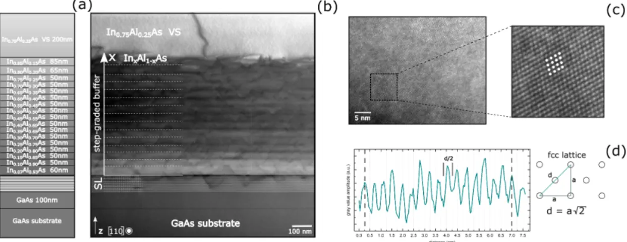
4.2 Postgrowth crystal characterisation methods . . . . 39
4.2.1 Secondary ion mass spectroscopy . . . . 39
4.2.2 Transmission electron microscopy . . . . 39
4.2.3 Atomic force microscopy . . . . 40
4.3 Electric transport measurements . . . . 40
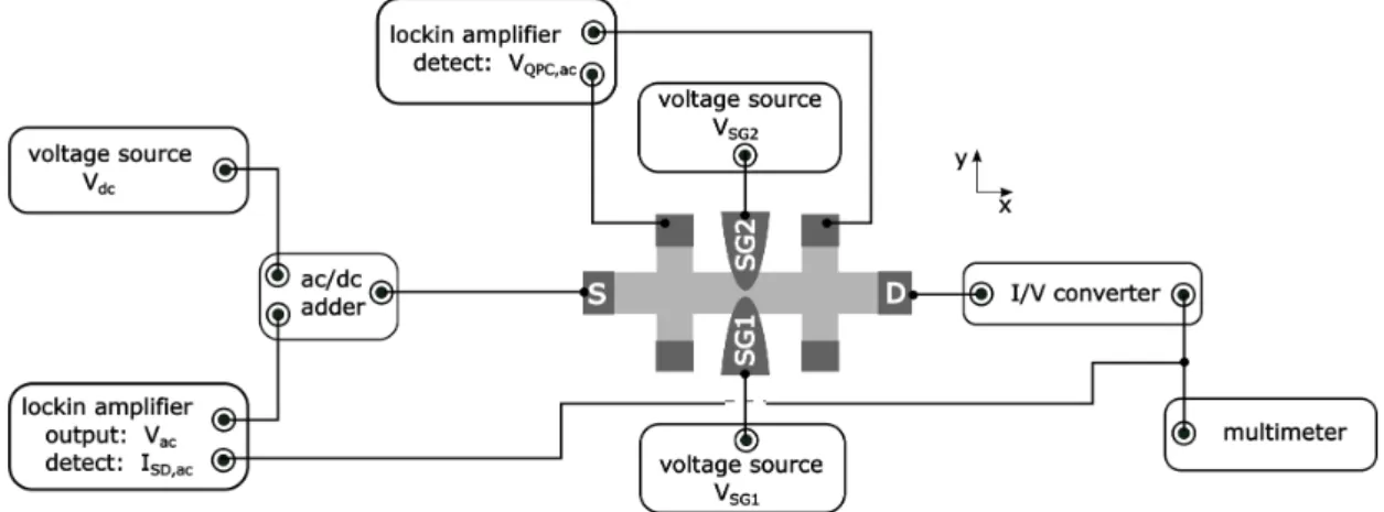
4.3.1 Device design . . . . 40
4.3.2 Measurement setups . . . . 44
5 Design and characterisation of InGaAs/InAlAs systems . . . . 45
5.1 Buffer layer growth . . . . 45
5.2 Design of InGaAs/InAlAs active layer systems . . . . 49
5.3 Discussion and conclusion . . . . 55
5.4 Comment on other material systems . . . . 57
III Study of 1D and 2D transport characteristics 6 Realization of conductance quantization in InGaAs/InAlAs . . . 61
6.1 Finger-gate layout . . . . 61
6.2 2D and 1D transport in the model system GaAs/AlGaAs . . . . 64
6.2.1 2D magnetotransport properties . . . . 64
6.2.2 1D transport in SG-defined QPCs . . . . 66
6.2.3 Conclusion . . . . 72
6.3 1D transport in InGaAs/InAlAs systems . . . . 73
6.3.1 1D transport in SG-defined QPCs . . . . 73
6.3.2 1D transport in TrG-defined QPCs . . . . 79
6.4 Conclusion and discussion . . . . 87
7 Gating response of various III-V heterostructures . . . . 89
7.1 Sample fabrication and MT measurement sequence . . . . 90
7.2 Chemical treatment and different surface terminations . . . . 91
7.2.1 5nm In0.75Ga0.25As cap . . . . 91
7.2.2 2.5nm In0.75Ga0.25As cap . . . . 94
7.2.3 Charge transfer model . . . 101
7.2.4 In0.75Al0.25As surface termination . . . 112
7.2.5 Conclusion . . . 115
7.3 Post-deposition thermal annealing . . . 117
7.3.1 Gating responses of annealed samples I - L . . . 117
Contents
7.4 Variation of the dielectric material . . . 121
7.5 Charge carrier mobility and scattering sources . . . 124
7.5.1 The charge carrier mobility . . . 125
7.5.2 The elastic mean free path . . . 128
7.6 Towards the reduction of InAlAs deep level donor states . . . 130
7.7 Conclusion . . . 131
8 Ballistic conductance in InGaAs/InAlAs-based systems . . . 135
8.1 Realization of robust ballistic 1D conductance . . . 136
8.1.1 Reproducibility . . . 136
8.1.2 Time stability . . . 138
8.1.3 Conclusion . . . 139
8.2 Tuning the ballistic conductance . . . 139
8.2.1 Variation ofVCG . . . 139
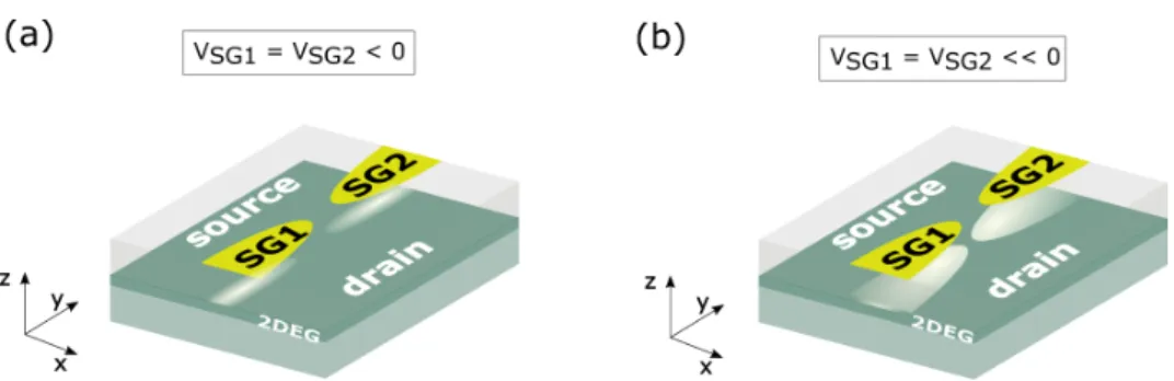
8.2.2 Asymmetric biasingVSG1≠VSG2 . . . 141
8.2.3 Conclusion . . . 143
8.3 1D conductance in alternative heterostructures . . . 143
8.4 Conclusion . . . 146
9 Signatures of Rashba-type spin-orbit interaction . . . 147
9.1 Gating response of undoped InGaAs/InAlAs heterostructure . . . 147
9.2 FFT of magnetooscillations . . . 148
9.2.1 Exemplary FFT in gating regime III . . . 149
9.2.2 Large magnetic field limit . . . 150
9.2.3 Semi-classical simulation of the magnetoresistivity . . . 152
9.2.4 Gate voltage dependence of FFT spectra . . . 155
9.3 Double-peak generation in FFT . . . 156
9.3.1 Size-quantization effects . . . 156
9.3.2 SOI effect . . . 159
9.4 SOI in undoped InGaAs/InAlAs systems . . . 159
9.4.1 SOI effects in magnetooscillations . . . 159
9.4.2 Evaluation of SOI strength . . . 160
9.4.3 FFT analysis . . . 160
9.4.4 Beating-node analysis . . . 162
9.4.5 Discussion . . . 163
9.4.6 Comparison to literature . . . 167
9.5 Conclusion . . . 168
10 Conclusion and outlook. . . 169
IV Appendix A Sample fabrication . . . 177
Contents
B Supplementary measurements . . . 181
B.1 1D and 2D transport measurements . . . 181
B.2 Estimation of the quantum lifetime . . . 185
B.3 Determination of SOI strength . . . 186
Bibliography . . . 187
Acknowledgments . . . 203
Introduction
1
In 1988, two groups from Delft [1] and Cambridge [2] reported their historical discovery that the resistance of a Sharvin-type point contact, which they both implemented in a GaAs/AlGaAs heterostructure, does not change continuously when the width of the constriction is reduced. Instead, they found distinct steps in the resistance and conductance curves to appear. Van Wees et al. [1] concluded their publication with the solemn words:
"A novel quantum effect is found: The conductance is quantized in units of 𝑒2/𝜋~."
This finding constitutes a profound experimental confirmation of the Landauer formula, already suggested in 1957 by Rolf Landauer [3], which was later generalized to the Landauer-Büttiker formula [4]. Since then, in addition to GaAs-based electron systems [5–9], conductance quantization has been realized in many other material systems as, e.g., GaN/AlGaN heterostructures [10], AlAs [11], InGaAs [12–16], InAs [17–20], InSb [21]
and Si/SiGe systems [22–24].
When considering such quantization effects in 1D in the context of materials with strong spin-orbit interaction, new research fields have opened up as, for example, the high-topical field of topological quantum computation [25–29]. Therein, the coupling of a high- mobility 2D electron gas with large spin-orbit interaction to an s-wave superconductor presents a fundamental part. In these experiments, quantum point contacts are employed to measure the quantized conductance doubling - a manifestation of proximity-induced superconductivity in the 2D electron system [30, 31]. To follow the theoretical recipe for the creation of a spinless p-wave superconductor in which a single isolated Majorana state arises [27, 28], quantum point contacts generate the required 1D subband structure [30, 31].
As a second example, the physics of quantum point contacts has fueled a variety of device applications and concepts [13, 16, 19, 32, 33], merging under the roof of spinorbitronics [34]. One goal is the realization of a spin-transistor. This requires the implementation of three key components to yield a fully functional system, i.e. a spin injector, a spin detector and a tuning knob to manipulate the spin current between injection and
1 Introduction
detection. Realizing the proposed spin-transistor generally entails two main manufacturing challenges: Firstly, using ferromagnetic electrodes for the generation and read-out of the spin-polarized current, one is usually subjected to the conductance mismatch. Secondly, spin-dephasing mechanisms inside the transistor channel impede a loss-free transmission of spin-information. In an elegant, ballistic and all-electric spin-transistor concept presented by Chuang et al. [13], these obstacles are readily eliminated. Therein, two serial quantum point contacts, which are implemented in a 2D electron gas, are employed as a spin injector and spin detector by adjusting the strength of lateral spin-orbit coupling inside the 1D channel. By exploiting Rashba-type spin-orbit interaction, the spin precession between spin injector and detector can be manipulated with an external electric field, applied via a middle-gate electrode.
Given the examples outlined above, it is interesting to note that the key requirements for topological quantum computation and the spinorbitronic device application are very similar: Achieving large spin-orbit coupling in a highly mobile electron system with a clean semiconductor surface. In this regard, InAs/InGaAs-based heterostructures offer inherent advantages in their material properties, like a low effective mass, a large Landé g-factor, as well as large Rashba spin-orbit interaction, making them attractive candidates for these device applications. In addition to all of that, the absence of a Schottky barrier for sufficiently large indium concentrations enables the fabrication of metal-semiconductor interfaces with unique transparency. To harvest the undeniable potential of this semiconductor system, material specific challenges have to be met. This thesis focuses on those perspectives of the InAs-based material system which would qualify it as a reliable platform for the realization of reliable 1D spinorbitronic devices.
Due to the lack of a lattice-matched substrate for InAs and InGaAs with arbitrary indium concentration, sophisticated buffer layer concepts have to be implemented during the molecular beam epitaxy to achieve highly mobile electron systems [35–38]. Furthermore, InAlAs, which is commonly applied as a high-band gap material in InAs/InGaAs layer structures, introduces a significant arsenic-related background impurity density into the system, which at the same time provides free charge carriers for the InAs/InGaAs 2D system and thereby acts as an intrinsic dopant [37, 39]. On the upside, this yields the advantage that the epitaxial incorporation of a modulation doping layer into the system, which generally impedes the ballisticity of a 2D electron system, is not mandatory. On the downside, the doping-providing and thus ionized InAlAs defect states introduce a Coulombic disorder potential in the barrier layers surrounding the 2D electron gas, whereby 1D transport is likely to be affected. Except for their doping properties, InAlAs defect states have been scarcely addressed in the literature so far. Evaluating their impact on the implementation of 1D spinorbitronic devices in these material systems is a central part of this thesis, since a holistic study is not available yet.
Last but not least, a very elementary manufacturing challenge has to be met in III-V systems: GaAs and InAs, as well as their ternary compound systems InxGa1-xAs lack an electrically stable and defect-free oxide, which forms at the surface and influences the gating response of the system [40, 41]. This entails the need for elaborated device fabrication processes to avoid opacity of the semiconductor interface, being severely
detrimental for 2D electron systems proximitized to a superconductor, as well as to prevent hysteretic effects when the material system is gated.
From the above considerations it is apparent that a profound and comprehensive understand- ing of the electrostatic properties of the employed hybrid semiconductor/insulator/metal system is essential en route to spinorbitronic and topological applications. With our work, we intend to contribute to the current investigations in this quite extensive field of research.
This thesis is organized as follows:
In chapter 2, we briefly introduce the fundamental concepts of the herein analysed 2D and 1D transport characteristics in external electric and magnetic fields.
Chapter 3 summarizes relevant aspects of band-related spin-orbit interaction, especially in 2D electron systems. Furthermore, we address the spin-transistor concept as presented in [13].
The structural and electrical characterisation methods used in this thesis are shortly introduced in chapter 4.
In chapter 5, we summarize the key results of our epitaxial study, where we growth- engineer our active layer system. The heterostructures are structurally analysed and their magnetotransport properties are then tested with respect to their suitability for spinorbitronic device application.
Chapter 6 is devoted to the realization of quantized conductance in the In0.75Ga0.25As/
In0.75Al0.25As layer system. Thereby, we test a split-gate design on the model system GaAs/Al0.31Ga0.69As. We then provide a thorough study of the transport in electrically defined quantum point contacts in the non-illuminated and illuminated state in the material system InGaAs.
Based on the experimental results of the preceding chapter, we discuss the gate response of several different metal/dielectric/semiconductor material combinations in the top-gated Hall bar measurements in chapter 7. We introduce a holistic charge transfer model, which is able to describe the electric transport properties under gating over a wide bias and electron density range.
At this point, our detailed understanding of the material system allows us to demonstrate the realization of robust ballistic conductance in different In0.75Ga0.25As/In0.75Al0.25As active layer systems in chapter 8.
Chapter 9 addresses the peculiar magnetooscillations, which appear when we gate our system. From these experiments, we are able to estimate the strength of Rashba spin-orbit interaction in our heterostructures.
Chapter 10 concludes and evaluates the experimental results by means of their implications on device applications.
The appendix IV yields supplementary information to sample fabrication and auxiliary transport measurements in one and two dimensions.
1 Introduction
I
2 Fundamental concepts of 2D and 1D elec-
tric transport . . . . 7 2.1 The two-dimensional electron gas . . . . 7 2.2 Ballistic electron transport in a 1D channel . . . . 16
3 Fundamental concepts of spin-orbit inter-
action . . . 23 3.1 SOI in 2D systems . . . . 24 3.2 Evaluation of SOI strength . . . . 27
Theoretical background
Fundamental concepts of 2D and 1D electric transport
2
This chapter briefly introduces the fundamental concepts of electric transport in band structure-engineered semiconductor heterostructures in external electric and magnetic fields. Therein, we give the relevant expressions for 2D and 1D electric transport, which we will utilise in the course of this thesis.
2.1 The two-dimensional electron gas
The dispersion relation of an electron in a crystal lattice can be derived by means of k·p-perturbation theory from the Bloch equation. By introducing the electron effective mass𝑚∗as
1 𝑚∗
= 1 𝑚𝑒
1+ 2𝑚𝑒𝑃2
~2
,
with~=ℎ/2𝜋 being the reduced Planck constant, the dispersion relation of thenearly free electronin a bulk crystal near theΓ-point can be described with
𝐸𝑐(k) ≈ 𝐸𝑐+~2𝑘2 2𝑚∗
, (2.1)
where𝐸𝑐is the lower edge of the conduction band. The band edge parameter 𝑃can be considered as the expectation value of the momentum in the vicinity of theΓ-point.
In the course of this thesis, we will analyse the electric transport in band structure- engineered semiconductor heterostructures. The thereby introduced band discontinuities, which present a perturbation to the periodic lattice potential, enable the confinement of the electron’s motion in the semiconductor crystal. This perturbation of the translational invariance in one direction, for example the𝑧-direction, can be treated in the framework of the envelope function approximation (EPA). Due to the still maintained translational invariance in the directions𝑥 and𝑦 perpendicular to the confinement direction, the wave functionΨ(r)of the electron can be decomposed intoΨ(r) =𝜓(𝑥 , 𝑦)𝜒(𝑧). By means of
2 Fundamental concepts of 2D and 1D electric transport
this ansatz and the appropriate boundary conditions, one finds that the energy spectrum in the𝑧-direction is quantized and can be described via discrete subband states 𝜒𝑛(𝑧), where𝑛is the corresponding quantum number. The total energy dispersion relation then reads as
𝐸 =𝐸𝑛(𝑘k) +~2𝑘2
k
2𝑚∗
, (2.2)
where 𝑘k = q
𝑘2
𝑥 +𝑘2
𝑦 is the in-plane wave vector. If only the lowest subband is occupied one commonly refers to the system as a two-dimensional electron gas (2DEG). The resulting density of states (DOS) of the 2DEG is
D2𝐷(𝐸) = 𝑔𝑠𝑔𝑣𝑚∗ 𝜋~2
,
with𝑔𝑠 being the degree of spin degeneracy and𝑔𝑣represents the valley degeneracy. For In0.75Ga0.25As/In0.75Al0.25As heterostructures, we generally apply𝑔𝑠 =2 and𝑔𝑣 =1. The sheet carrier density𝑛𝑠 of the 2DEG can be expressed as
𝑛𝑠 =D2𝐷(𝐸) ·𝐸𝐹,
where𝐸𝐹 is the Fermi energy, referring to the highest occupied energy state of the system.
Thus, the corresponding Fermi wave vector𝑘𝐹 is given by
𝑘𝐹 =
r2𝑚∗𝐸𝐹
~2
= p
2𝜋𝑛𝑠 . (2.3)
2.1.1 Drude model
A basic theoretical model for the description of the motion of electrons in a crystal is provided by the Drude model [42, 43]. In this semiclassical description, the electrons are described as classical particles, that undergo collisions inside the crystal after an average scattering time𝜏𝑡𝑟 when moving in an external electric field. In between two subsequent scattering events, an electron gains on average the so-called drift velocityv𝐷. The current densityjis determined as
j = 𝜎E = −𝑒𝑛𝑠𝜇E = −𝑒𝑛𝑠v𝐷 , (2.4) with𝜎being the conductivity and𝜇= |𝑒|𝜏𝑡 𝑟
𝑚∗ is the electron mobility.
The motion of an electron, which is subjected to an additional magnetic field, is described by
𝑚∗ 𝜏𝑡𝑟
v𝐷 = −𝑒(E+v𝐷 ×B). (2.5)
In the case of|B| ≠ 0,𝜎 transforms into a tensor. By choosing B = (0,0, 𝐵), we can
2.1 The two-dimensional electron gas
write the current density as 𝑗𝑥
𝑗𝑦
=
𝜎𝑥 𝑥 𝜎𝑥 𝑦 𝜎𝑦𝑥 𝜎𝑦 𝑦
· 𝐸𝑥
𝐸𝑦
= 𝜎0 1+𝜔2
𝑐𝜏2
𝑡𝑟
·
1 −𝜔𝑐𝜏𝑡𝑟 𝜔𝑐𝜏𝑡𝑟 1
· 𝐸𝑥
𝐸𝑦
, (2.6) with the Drude conductivity
𝜎0=𝑛𝑠𝑒2 𝜏𝑡𝑟 𝑚∗
=𝑛𝑠𝑒 𝜇 and the cyclotron frequency
𝜔𝑐 = 𝑒 𝐵 𝑚∗
.
By tensor inversion of the conductivity tensor, we gain the corresponding resistivity tensor: 𝜎 =𝜌−1. It can be shown that the components yield the following form:
𝜌𝑥 𝑥 =𝜌𝑦 𝑦 = 𝜎𝑥 𝑥 𝜎2
𝑥 𝑥 +𝜎2
𝑦 𝑦
= 𝑚∗
𝑒2𝑛𝑠𝜏𝑡𝑟 (2.7)
𝜌𝑥 𝑦 =−𝜌𝑦𝑥 =
𝜎𝑥 𝑦 𝜎𝑥 𝑥2 +𝜎𝑦 𝑦2
= 𝐵
|𝑒|𝑛𝑠
. (2.8)
Measuring 𝜌𝑥 𝑥 and 𝜌𝑥 𝑦 independently from each other in a magnetotransport (MT) measurement thus yields the sheet carrier density𝑛𝑠 and the corresponding charge carrier mobility𝜇, which characterise the transport properties of a 2DEG:
𝑛𝑠 = 𝑒· 𝜕 𝜌𝑥 𝑦
𝜕 𝐵 𝐵=0
!−1
(2.9)
𝜇 =
𝑒·𝑛𝑠𝜌𝑥 𝑥(𝐵=0)−1
. (2.10)
Different device geometries can be employed to determine𝑛𝑠and𝜇in a MT measurement.
This will be subject of section 4.3. Depending on the sample geometry and also on the applied evaluation method, we will distinguish between 𝑛𝑣 𝑑𝑃, 𝑛𝐻 𝑎𝑙 𝑙 and 𝑛𝑆 𝑑𝐻 as introduced in the following sections.
An important length scale in the regime of diffusive - and also ballistic - transport is the elastic mean free path𝑙𝑚 𝑓 𝑝, which can be expressed as
𝑙𝑚 𝑓 𝑝 =𝑣𝐹𝜏𝑡𝑟 = ~ 𝑒
p2𝜋𝑛𝑠𝜇 , (2.11)
where𝑣𝐹 = ~𝑚𝑘∗𝐹 is the Fermi velocity . Parallel transport
In the Drude model multisubband occupation and parallel conduction can be described as a sum of the currents of all participating transport channels [44, 45]. Thus, the total
2 Fundamental concepts of 2D and 1D electric transport
conductivity 𝜎𝑡 𝑜𝑡 of the system can be expressed in the form of a summation over all contributing sheet conductivities𝜎𝑖, where𝑖 labels the individual transport channel:
𝜎𝑡 𝑜𝑡 = 𝜎1 + 𝜎2+ ...=Õ
𝜎𝑖 , (2.12)
with
𝜎𝑖 =
𝑛𝑖𝑒2𝜏𝑡𝑟 ,𝑖 𝑚∗
𝑖
· 1
1+𝜔2
𝑐𝜏2
𝑡𝑟 ,𝑖
·
1 −𝜔𝑐𝜏𝑡𝑟 ,𝑖 𝜔𝑐𝜏𝑡𝑟 ,𝑖 1
. (2.13)
Inversion of the expression (2.12) for the total conductivity𝜎𝑡 𝑜𝑡 yields the corresponding term for the total resistivity𝜌𝑡 𝑜𝑡 of the system.
The case of two non-interacting transport channels, labeled with the indices 1 and 2, yields in the limit of small magnetic fields when following simplified expressions for𝜌𝑥 𝑥 and𝜌𝑥 𝑦:
𝜌𝑥 𝑥 = 1 𝑒
· 1
𝑛1𝜇1+𝑛2𝜇2
= 1 𝑒
· 1
𝑛𝐻 𝑎𝑙 𝑙 ·𝜇𝐻 𝑎𝑙 𝑙 (2.14)
𝜌𝑥 𝑦 = 𝐵 𝑒
·
𝑛1𝜇2
1+𝑛2𝜇2
2
(𝑛1𝜇1+𝑛2𝜇2)2 = 𝐵 𝑒
· 1 𝑛𝐻 𝑎𝑙 𝑙
. (2.15)
It is reasonable to assume, that the mobility𝜇2of a newly populated, higher subband is much lower than the mobility𝜇1of the ground (first) subband, i.e. 𝜇2 𝜇1[46]. In this case, the above expression (2.15) for𝜌𝑥 𝑦 can be further simplified to
𝑛𝐻 𝑎𝑙 𝑙 = (𝑛1𝜇1+𝑛2𝜇2)2 𝑛1𝜇2
1+𝑛2𝜇2 2
≈ (𝑛1𝜇1+𝑛2𝜇2)2 𝑛1𝜇2
1
. (2.16)
This expression shows that the measured Hall density contains the individual charge densities of the contributing channels, whose density values are further weighted by the mobility of the respective channel.
2.1.2 The quantum Hall effect
For sufficiently high magnetic fields, i.e. 𝜔𝑐𝜏𝑡𝑟 1, the description of the magneto- transport in a 2DEG within the semiclassical Drude model breaks down. As was first addressed by Landau [47], the corresponding Hamiltonian for electrons in a 2DEG, which are subjected to an external magnetic field, reads as
H = (p+ |𝑒|A)2 2𝑚∗
+𝑉(𝑧), (2.17)
where𝑉(𝑧)is the confinement potential andAis the vector potential. In Landau gauge, A can be written as A = (0, 𝐵𝑥 ,0) withB = (0,0, 𝐵). With the ansatzΨ(𝑥 , 𝑦, 𝑧) = 𝑢(𝑥)𝑒𝑖 𝑘𝑦𝑦𝜒(𝑧)for the electron wave function, the problem can be reduced to the form of a
2.1 The two-dimensional electron gas 1D quantum mechanical harmonic oscillator. The quantized energy states𝐸𝑛
𝑥 𝑦 are given by
𝐸𝑛
𝑥 𝑦 =~𝜔𝑐
𝑛𝑥 𝑦+ 1 2
, (2.18)
with𝑛𝑥 𝑦 being the Landau quantum number. All states with different𝑘𝑦 inside a Landau level𝑛𝑥 𝑦are energetically degenerate. By means of periodic boundary conditions for𝑘𝑦, the number of states in a Landau level per unit area are determined as
𝑛𝐿 = |𝑒|𝐵 ℎ
. (2.19)
For a given electron density𝑛𝑠, the Landau level filling factor𝜈, which is the amount of populated Landau levels at a given magnetic fieldB, is calculated with
𝜈 = 𝑛𝑠 𝑛𝐿
. (2.20)
Oscillatory magnetoresistance
In the case of a constant 2D charge density𝑛𝑠, the magnetic field dependence of the DOS of a Landau level manifests itself in an oscillatory behavior of 𝐸𝐹. Correspondingly, this results in a sinusoidal oscillation of the magnetoresistivity 𝜌𝑥 𝑥 in 1/𝐵, the so-called Shubnikov-de Haas oscillations. A semi-classical description of 𝜌𝑥 𝑥(𝐵)was first given by Coleridge et al. [48]:
Δ𝜌𝑥 𝑥 =𝜌0+4·2𝜋 𝑘𝐵𝑇 𝑚∗
~𝑒 𝐵
· 1
sinh2𝜋 𝑘~𝐵𝑒 𝐵𝑇 𝑚∗
·exp
−𝜋𝑚∗ 𝑒 𝜏𝑞
· 1 𝐵
·cos2𝜋E𝑚∗
~𝑒
· 1 𝐵
−𝜋
, (2.21) withE = 𝐸𝐹 − 𝐸𝑛, where𝐸𝑛is the energy of the nth subband and𝑘𝐵 is the Boltzmann constant. 𝜏𝑞 is the quantum lifetime, which is also often referred to as single particle lifetime. It specifies the lifetime of the quantum state, i.e. the time, in which one is able to define an electronic momentum eigenstate in the system in the presence of scattering.
We can identify the second term in equation (2.21) as a description of the temperature- dependent DOS of the Landau levels with a Lorentzian energy broadening, introduced by scattering. Therein, the exponential term exp
− 𝜋𝑚∗
𝑒 𝜏𝑞
· 1
𝐵
, which is commonly referred to as theDingle factor, determines the magnitude of the Shubnikov-de Haas oscillations [43, 49–51].
In high-mobility samples𝜏𝑞can be more than ten times smaller than the transport lifetime 𝜏𝑡𝑟. This is due to the fact that the single particle lifetime𝜏𝑞takes every scattering event into account, irrespective of the scattering angle 𝜙. It is described by
1 𝜏𝑞
= 𝑚∗
~2
∫ 2𝜋 0
𝑊(𝜙)𝑑 𝜙 2𝜋 ,
2 Fundamental concepts of 2D and 1D electric transport
wherein𝑊(𝜙)is the scattering cross section into a particular direction. For high-mobility systems, however, small-angle scattering predominates. In the description of the transport lifetime𝜏𝑡𝑟, which determines the mobility in a system, large-angle back-scattering is more strongly weighted since it leads to a significant change of the momentum direction [43, 50–52]:
1 𝜏𝑡𝑟
= 𝑚∗
~2
∫ 2𝜋
0
𝑊(𝜙) (1−cos(𝜙))𝑑 𝜙 2𝜋 .
When the Fermi level lies in between two subsequent Landau levels and negligible scattering of charge carriers into neighboring, extended energy states takes place, we find a minima in the longitudinal resistivity of the system. A maximum in𝜌𝑥 𝑥(𝐵)arises when the Fermi level passes the center of the DOS of the topmost Landau level. Consequently, by means of the above expression (2.21), the sheet density 𝑛𝑠 of the 2DEG can be determined by evaluating the neighboring minima of the Shubnikov-de Haas oscillations in 1/𝐵via following relation:
Δ 1
𝐵
= 1 𝐵𝑖+1
+ 1 𝐵𝑖
= 2|𝑒| ℎ𝑛𝑠
. (2.22)
Within this thesis, values of𝑛𝑠, which are determined via this formula from the Shubnikov- de Haas oscillations, are labeled as𝑛𝑆 𝑑𝐻.
The integer quantum Hall effect
Simultaneously to the appearance of the Shubnikov-de Haas oscillations in the longitudinal magnetoresistivity 𝜌𝑥 𝑥(𝐵), well-pronounced plateaus in the transversal resistivity 𝜌𝑥 𝑦 emerge. This presents the so-calledquantized Hall effect [53, 54]. Therein, steps in 𝜌𝑥 𝑦(𝐵)arise at specific resistivity values, which are given by
𝜌
𝑝𝑙 𝑎𝑡 𝑒 𝑎𝑢
𝑥 𝑦 = 1
𝑝 ℎ 𝑒2 = 1
𝑝
𝑅𝐾, (2.23)
with 𝑝 ∈ N\{0}. 𝑅𝐾 = 25812.807Ω is the well-knownvon Klitzing constant. Conse- quently, plateaus in𝜌𝑥 𝑦 occur when the Landau level filling factor is close to an integer value of𝜈. Utilising the relations (2.7) and (2.8) in order to calculate the corresponding components of the conductivity tensor at the Hall plateau values, we find:
𝜎
𝑝𝑙 𝑎𝑡 𝑒 𝑎𝑢
𝑥 𝑥 = 0 (2.24)
𝜎
𝑝𝑙 𝑎𝑡 𝑒 𝑎𝑢
𝑥 𝑦 = 𝑖
𝑒2 ℎ
. (2.25)
This means that in the case of an integer value of𝜈, the transversal Hall conductance is quantized in units of𝑒2/ℎ, which is the so-calledconductance quantum.
In the Landauer-Büttiker picture [4], the conductance quantization can be well described as the perfect transmission of one-dimensional edge channels between the source and
2.1 The two-dimensional electron gas the drain contact. Due to the spatial separation of the edge channels at the opposing Hall bar interfaces, these counterpropagating channels do not interact since energy states inside the Hall bar region are localized. Each (spin-degenerate) edge channel contributes a conductance of 2𝑒2/ℎto the total conductance of the system.
Zeeman effect
An external magnetic fieldB, which breaks the time reversal symmetry, lifts the spin degeneracy. The corresponding Hamiltonian can be written as
H𝑍 = 1
2𝑔∗𝜇𝐵𝝈·B, (2.26)
with the Pauli matrices𝝈and𝜇𝐵 being the Bohr magneton. For bulk semiconductors, in first order, the energetical Zeeman splittingΔ𝐸𝑍 is isotropic in space and can be described with
Δ𝐸Z=𝑔∗𝜇𝐵𝐵 , (2.27)
where𝑔∗ is the effective Landé g-factor. Thus, the spin-splitting strength is not only proportional to the applied magnetic field 𝐵, but also to the prefactor𝑔∗. Deviations from the free-electron g-factor arise due to a coupling of the electron’s spin to the angular lattice-periodic part of the Bloch wave functions. For a system with reduced symmetry, for example due to spatial confinement, and which additionally lacks bulk inversion asymmetry,𝑔∗ has to be described by a tensor. The in- and out-of plane anisotropy arises from thek·p-coupling between different subbands. The in-plane anisotropy is predicted to be proportional to built-in electric fields in the system and scales with the strength of the Dresselhaus contribution to spin-orbit interaction [55].
As we find later in chapter 3, the Dresselhaus contribution to spin-orbit coupling can be neglected in our analysed heterostructures. Furthermore, solely magnetic fields perpendicular to the sample surface are applied in the course of this work. We can therefore treat𝑔∗ as a scalar in order to give an estimate of the Zeeman spin-splitting in our MT measurements.
Including the Zeeman spin-splitting from equation (2.27) into the description of the Landau level eigenstates in equation (2.18) yields the following expression:
𝐸𝑛
𝑥 𝑦 =~𝜔𝑐
𝑛𝑥 𝑦+ 1 2
± 1
2𝑔∗𝜇𝐵𝐵. (2.28)
Correspondingly, the energy spin-splitting of the Landau levels enters the description of the Landau level DOS, which thus provokes a modification of the periodicity of the Shubnikov-de Haas oscillations for sufficiently high magnetic fields. Since in the spin-split case the factor of two in equation (2.22) does not have to be included anymore, a transition of the 1/𝐵-periodicity of the magnetooscillations from a frequency 𝑓 to a frequency 2𝑓 can be observed (as long as the description by means of equation (2.21) sill holds).
2 Fundamental concepts of 2D and 1D electric transport
Magneto-intersubband scattering
In the case that an additional 2D electron system contributes to magnetotransport, the Fermi level crosses a second size-quantized subband. Thus, the description of the Shubnikov-de Haas oscillations by means of equation (2.21) has to be extended. According to equation (2.18), this second 2DEG contributes an additional set of Landau level eigenenergies to the B-field-dependent energy spectrum of the system. In first approximation, the respective resistivities 𝜌𝑥 𝑥 ,𝑖, where𝑖 =1,2 accounts for the two contributing 2D systems, can be described by means of equation (2.21), with the corresponding quantum lifetime𝜏𝑞,𝑖 and electron density𝑛𝑠,𝑖. In addition, a further effect in𝜌𝑥 𝑥(𝐵) can arise, which is generally referred to as themagneto-intersubband scattering effect (MIS). This term has been coined by the work of Raikh and Shabazyan [56]. In the case of two spatially non-separated 2DEGs, i.e. two size-quantized subbands of a QW for instance, this interaction effect has to be taken into account. As the name implies, MIS accounts for the increased intersubband scattering processes when the Landau levels of the two size-quantized subbands cross. This level crossing can be described by following energy-dependent relation:
𝐸1 + 𝐸𝐿 𝐿 ,1 =𝐸2 + 𝐸𝐿 𝐿 ,2 = 𝐸1 +𝐸1,2 + 𝐸𝐿 𝐿 ,2 . (2.29) 𝐸1 and 𝐸2 describe the onset of the first and second size-quantized subbands of the QW and𝐸1,2 = |𝐸1−𝐸2|represents the energy difference between the two subbands.
𝐸𝐿 𝐿 ,1 and 𝐸𝐿 𝐿 ,2 constitute the Landau level energies of the first and second subband, respectively. Inserting the (spin-degenerate) expression for the Landau level eigenstates of equation (2.18) into the above equation (2.29) yields
𝐸1 + ~𝜔𝑐
𝑛+ 1 2
= 𝐸1 +𝐸1,2 + ~𝜔𝑐
𝑚+ 1 2
(2.30)
⇒ (𝑛 − 𝑚) = 𝑚∗
~𝑒
·𝐸1,2· 1 𝐵
, (2.31)
with𝑛, 𝑚being the Landau level indices of the two size-quantized subbands, respectively.
Note that𝑛 > 𝑚is always true, so that (𝑛 − 𝑚) > 0. The latter equation can be viewed as a magnetic field-dependent condition for Landau level-crossing in a 2D system.
The modulation of𝜌𝑥 𝑥(𝐵)due to MIS was first correctly described by Coleridge [57] and was later refined by Leadley et al. [58] to
Δ𝜌𝑥 𝑥 𝜌0
= 𝐴1 hΔ𝑔1i
𝑔0
+𝐴2 hΔ𝑔2i
𝑔0
+𝐵12
hΔ𝑔1Δ𝑔2i 𝑔2
0
, (2.32)
with
Δ𝑔𝑖 𝑔0
=2𝜙(𝑇𝐷
𝑖)cos 2𝜋
𝐸𝐹 −𝐸𝑖
~𝜔𝑐 +𝜋
(2.33)