Determination of hole g-factor in InAs/InGaAs/InAlAs quantum wells by magneto-photoluminescence studies
Ya. V. Terent’ev,
1,2S. N. Danilov,
1M. V. Durnev,
2J. Loher,
1D. Schuh,
1D. Bougeard,
1S. V. Ivanov,
2and S. D. Ganichev
11
Physics Department, University of Regensburg, 93040 Regensburg, Germany
2
Ioffe Institute, 194021 St. Petersburg, Russia
(Received 7 October 2016; accepted 20 January 2017; published online 6 February 2017)
A circularly polarized magneto-photoluminescence (magneto-PL) technique has been applied to investigate the Zeeman effect in InAs/InGaAs/InAlAs quantum wells (QWs) in the Faraday geometry. Structures with different thicknesses of the QW barriers have been studied in the mag- netic field parallel and tilted with respect to the sample normal. The effective electron-hole g-fac- tor has been found by measurement of splitting of polarized magneto-PL lines. Land e factors of electrons have been calculated using the 14-band k p method, and the g-factor of holes was determined by subtracting the calculated contribution of the electrons from the effective electron- hole g-factor. Anisotropy of the hole g-factor has been studied applying the tilted magnetic field.
Published by AIP Publishing. [http://dx.doi.org/10.1063/1.4975353]
I. INTRODUCTION
Heterostructures based on InAs possess a series of unique properties caused by a narrow bandgap. These prop- erties include high carrier mobility and a strong spin-orbit interaction making the system a promising candidate for high frequency electronics, optoelectronics, and spintronics application. One of the most interesting objects in this area is type-I quantum wells (QWs) based on InAs/InGaAs/InAlAs two-step bandgap engineering, where the In content can be varied from 30% to 80%.
1Such structures exhibiting bright photoluminescence in the mid-infrared range
2,3demonstrate high-mobility two-dimensional electron gas (2DEG),
4–7pro- nounced spin-dependent optical,
3,8,9transport,
10–13and opto- electronic
14–16phenomena. Determination of Land e factors of both types of the carriers is the cornerstone for the studies of spin-related phenomena. As for InAs QWs, the electron g- factor in this type of heterostructure is well-studied by differ- ent techniques. To date, the reported values of the electron g-factor obtained by magneto-transport and terahertz experi- ments range from g
e¼ 3 to g
e¼ 9 depending on the In content in the QW barrier.
6,11,12Moreover, experimentally obtained Land e factors are consistent with the values calcu- lated in the framework of the k p method.
In contrast to electrons, determination of the hole g-factor g
his still a challenging task. There are no available experimental data as well as reliable theoretical calcula- tions. The picture becomes even more intriguing in light of the previous magneto-optical experiments.
3,8They indicate surprisingly small magnitude of the effective electron-hole g-factor, which is the difference between g
hand g
e.
Here, we report on studies of InAs/In
0:75Ga
0:25As/In
0:75Al
0:25As QW structures by polarization-resolved magneto- photoluminescence (magneto-PL), which enables direct mea- surement of the effective electron-hole g-factor. We have determined the Land e factor of holes combining obtained experimental data with theoretical calculations of an electron contribution. We have obtained the dependence of electron
and hole g-factors on the QW barrier width. We have investi- gated anisotropy of the hole g-factor in the tilted magnetic field and shown that the values of g
hin the tilted magnetic field are in agreement with prediction of close-to-zero hole Zeeman splitting in the magnetic field lying in the QW plane.
II. SAMPLES AND EXPERIMENTAL TECHNIQUE Experimental samples were fabricated by molecular beam epitaxy onto a fully relaxed In
xAl
1xAs/(001)GaAs graded buffer
3,17with a stepwise increase of the In content (x ¼ 0.05 to x ¼ 0.75) over 1 lm. The structure of the QW is sketched in the inset of Fig. 1. An In
0:75Ga
0:25As quantum size part embedded in between In
0:75Al
0:25As layers features a symmetrically inserted and compressively strained InAs QW of 4 nm. The samples were intentionally undoped and, therefore, do not contain high-conductivity degenerated two- dimensional electron gas (2DEG) in contrary to analogous InAs/InGaAs/InGaAs structures fabricated for magnetotran- sport measurements. The latter have an electron concentra- tion of about 10
12cm
2, which was measured by the Hall effect. For our InAs QWs, we found n-type of conductivity with the concentration about 10
11cm
2. A set of samples with the different thicknesses of In
0:75Ga
0:25As barrier a were grown, where a is set to 7, 2.5, and 0 nm. The corre- sponding structures are labeled A, B, and C.
Photoluminescence was excited by emission of a laser diode operating in the cw mode at wavelength k ¼ 809 nm and detected with a Fourier transform infrared (FTIR) spec- trometer. The laser beam was focused on a 1-mm diameter spot on the sample. The excitation intensity W
excwas 100 mW. An external magnetic field up to 6 T was applied per- pendicularly to the wafer or was inclined at an angle of 40
to the direction of sample growth. Photoluminescence emis- sion having a wave vector directed along the magnetic field was detected (Faraday geometry). The sample temperature was kept as low as 2 K. Right- and left-handed circular
0021-8979/2017/121(5)/053904/6/$30.00
121, 053904-1Published by AIP Publishing.
polarized emission spectra were recorded applying a quarter wave ZnSe Fresnel rhomb.
18,19III. EXPERIMENTAL RESULTS
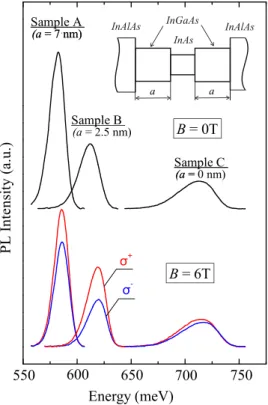
Bright PL was detected from all the samples. Its contour is close to the Gaussian function and slightly asymmetric being broadened at the low energy slope, see Fig. 1. The PL peak energy takes the value of 582.6 meV, 616.5 meV, and 713.6 meV in structures A, B, and C, respectively. So the PL peak energy increases with a decrease in the InGaAs barrier width. Emission intensity also varies in samples with differ- ent barrier widths and decays with its reduction. Both trends correlate with an increase in the PL peak full width at half maximum (FWHM) that takes the value of 18, 22, and 40 meV, in samples A, B, and C, respectively. Application of external magnetic field B in the direction perpendicular to the QW plane results in substantial changes in the PL spec- trum. It experiences magnetic-field-induced splitting into cir- cular polarized components, which is different in structures A, B, and C, see Fig. 2. Similar to the PL peak energy and FWHM, the splitting depends on the InGaAs barrier width. It is extremely small in structure A with the largest InGaAs barrier but is well-pronounced in sample C, where this layer is absent, taking an intermediate value in structure B. Interestingly, the splitting is a non-linear function of the magnetic field and its dependence on the magnetic field is different in all three samples; see Fig. 2. Note that minimal circular polarization of PL emission was detected in structure C while it possesses the largest splitting. The inclination of the magnetic field used for the analysis of g
hanisotropy critically diminishes
the splitting of a magneto-PL peak in samples B and C but does not affect it in sample A, see Fig. 2.
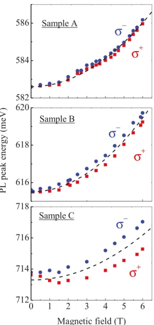
Besides the splitting of the PL contour into circular- polarized components, emission spectra experience blue shift, which corresponds to the diamagnetic shift of electron and hole energy levels in the magnetic field. The shift has a quadratic dependence on the magnetic field, see Fig. 3.
IV. DISCUSSION
The observed PL peak closely matches the calculated energy of direct optical transitions between the ground elec- tron e1 and the heavy hole hh1 subbands. The measured PL peak width in all the samples is 25 meV being larger than the estimated exciton binding energy (about a few meV).
20Note that, in general, both mechanisms of radiative recombi- nation are possible—exciton recombination and optical transi- tions between free-carrier states. Due to a relatively small value of exciton binding energy, identification of the dominant
FIG. 2. Zeeman splitting of the magneto-PL peak for structures A, B, and C with different widths of InGaAs barriers measured at the magnetic field perpendicular to the QW plane and tilted by
h¼40
with respect to the sample normal. Curves present polynomial fit to the experimental points.
Straight lines show a linear fit at small magnetic fields, which gives effective
g-factors of free carriers.FIG. 1. Photoluminescence spectra and circular-polarized magneto-PL spec-
tra of samples A, B, and C with different widths of InGaAs barriers, mea-
sured at magnetic field
B¼6 T perpendicular to the QW plane. The inset
shows the band diagram of the sample active region.
recombination mechanism is hardly possible. However, the type of optical recombination mechanism does not affect further logic and the main results of the study. Our analysis is made in the framework of the free-carrier recombination
model. Observed in experiment quadratic magnetic field dependence of the PL peak diamagnetic shift (Fig. 3) indicates Coulomb localization of the photoexcited carriers
21,22and greatly exceeds analogous dependence for an exciton in InAs.
In our structures, photo-carriers can be trapped to localization centers, which emerge due to inhomogeneity of the InAs QW or the presence of charged centers at the interfaces of the QW.
Detected splitting of PL lines in two circular polarizations reflects spin splitting of conduction and valence bands and it is described by effective electron-hole g-factor g
eff. Parameter g
effis equal to the difference of g-factors of the carriers that take part in the optical recombination, g
eff¼ g
hg
e, which corresponds to the splitting between r
þand r
PL lines.
In this formula and in the following, we assume that g
e> 0 when the energy of þ1=2 electron is higher than that of 1=2, and g
h> 0 when the energy of þ3=2 electron is higher than that of 3=2 in the electronic representation. The value of g
effcan be obtained directly from the Zeeman splitting in the linear region (see Fig. 2). The extracted values of g
effas a function of InGaAs barrier width are presented in Fig. 4 and Table I. It is clearly seen that the absolute value of g
efftends to increase with the decreasing width of the InGaAs barrier.
Although the observed nonlinear character of Zeeman splitting in the magnetic field B ⲏ 2 is out of scope of the pre- sent paper, it is worth mentioning that highly nonlinear Zeeman splitting of excitons was also detected in AlGaAs/
GaAs and InGaAs/GaAs systems and the model was sug- gested that is based on a spin-dependent field-induced admix- ture between the light- and heavy-hole valence bands.
23The large FWHM of the PL peak and its decay detected in sample C are explained in terms of effective scattering by charged centers at QW interfaces. In this structure, QW interfaces are formed by InAs and InAlAs layers having a large lattice mismatch and therefore are characterized by large defect density. Apparently scattering on these defects is responsible for the strong decay of optical recombination efficiency, increase of FWHM, as well as depolarization of the emission in the case of the magnetic field applied.
Now, we turn to separate determination of electron and hole g-factors. It was found that the g-factor of the hole is
FIG. 3. Circular polarized PL peaks energies as a function of magnetic field.
Curves present parabolic fitting
E¼adiaB2of the diamagnetic shift of PL lines, which is determined as a half-sum of the
rþand
rcomponents. The values of
adiaare listed in Table I.
FIG. 4.
g-factors in samples under study: squares represent the experimen-tally measured effective electron-hole
g-factorgeff, the solid line stands for the theoretically calculated electron
g-factor, and circles show the heavy-hole
g-factor derived using formulagh¼geffþge.
TABLE I. The values of electron and hole
g-factors (geff,
ge,
gh) and dia- magnetic shifts (a
dia) extracted from the analysis of experiment. The values
geand
ghare derived using Eq. (3) from the analysis of Zeeman splitting in the tilted magnetic field.
Sample A Sample B Sample C
geff 1.4 2.6 6.3
ge 11 10.7 8.4
gh 12.4 13.3 14.7
ge
…
9 13.2gh
…
9.4 15.8adia
(meV/T
2) 0.095 0.11 0.08
extremely sensitive to the separation between heavy-hole and light-hole quantization levels, which in turn depends on the unknown strength of strain fields and localization poten- tial. Hence, we only calculate g
e, which is less affected by the localization potential and strain, and therefore can be evaluated with much higher accuracy. Then, we estimate the value of g
husing experimentally determined g
effand
g
eff¼ g
hg
e: (1) The computation method is based on the numerical diagonali- zation of the 14-band k p Hamiltonian in the presence of the magnetic field.
24,25We use the 14-band k p-model, devel- oped in Ref. 24, for the calculation of electron and hole states at a zero magnetic field and use the obtained wave functions to calculate the Zeeman splitting at small magnetic fields in the framework of perturbation theory (the approach is analo- gous to the one used to calculate heavy-hole and light-hole g-factors in the framework of Luttinger Hamiltonian, see Eqs.
(9a) and (9b) of Ref. 25). The band parameters of InAs and its alloys were taken from Refs. 26 and 27, and confining poten- tials for electron and holes were calculated using the model of Ref. 27 taking into account elastic strain present in the struc- ture. The interband matrix elements of the momentum opera- tor were taken from Ref. 28.
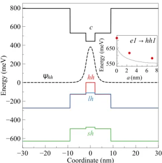
The evaluated band diagram, wave function of heavy hole at zero in-plane momentum k
k¼ 0, and optical transi- tions energies are presented in Fig. 5. The theoretical model gives close-to-experiment values of optical transitions ener- gies and the in-plane electron mass m
e(m
e¼ 0:038 m
0as determined from transport measurements in similar struc- tures
4,6,10). It also provides a good agreement between theo- retical and experimentally measured values of g
e.
6,10,29The discrepancy between theoretically calculated and experimen- tal values of optical transitions energies is possibly attributed
to the presence of in-plane localization potentials, which leads to the increase in the PL peak energy.
Evaluated values of hole Land e factors g
has well as the- oretical values of g
eand experimentally measured g
effare presented in Fig. 4 and Table I. As mentioned above, theoret- ical calculations do not allow us to obtain g
hwith sufficient precision. Its values obtained in the framework of the 14-band k p-model, used for evaluation of g
e, lie in the range of g
h¼ 2 to 8 for the studied structures
29and differ significantly from those given in Table I.
In order to study anisotropy of the hole g-factor, we have carried out experiments in a tilted magnetic field. The spin splitting of a heavy hole bound to the QW potential must be sensitive to a normal component of magnetic field only, because the in-plane heavy-hole g-factor is close to zero in III–V quantum wells.
30Moreover, the electron Zeeman splitting in quantum wells is also anisotropic.
31–33However, whereas the anisotropy of the electron g-factor tensor is controlled by the confinement and electron den- sity,
34,35the close-to-zero value of the heavy-hole in-plane g-factor is an intrinsic property of III–V quantum wells, which follows from the symmetry considerations that the mixing of þ3=2 and 3=2 states by the in-plane magnetic field is reduced.
30,36Therefore, in our simple model, we will neglect the anisotropy of the electron g-factor tensor keeping in mind that it is small compared to the anisotropy of the heavy-hole one. Note that the anisotropy would result in a slight decrease of the estimated value of the effective electron-hole g-factor in the tilted magnetic field.
The tilted magnetic field results in modification of g
eff. Indeed, the heavy-hole g-factor in a magnetic field tilted by an angle h with respect to QW normal is
~
g
hðhÞ ¼ ffiffiffiffiffiffiffiffiffiffiffiffiffiffiffiffiffiffiffiffiffiffiffiffiffiffiffiffiffiffiffiffiffiffiffiffiffiffiffiffiffi g
2hcos
2h þ g
2h;ksin
2h q
; (2)
where g
hand g
h;kare the components of the g-factor tensor for B parallel to the growth axis z k ½001 and B oriented in the plane of QW. Since g
h;kis close to zero, g ~
hg
hcos h and its absolute value must be reduced at h 6¼ 0.
For example, the 40
tilt of the field is expected to result in reduction of g
hfrom 13.3 and 14.7 to 10.2 and 11.3 for samples B and C, respectively. In turn, assuming that g
eis independent of h, the value of g
effis predicted to change to 0.5 and 2.9 for these samples. Comparison with Fig. 2 shows that these estimated values are close to the val- ues observed in the experiment.
Anomalous behaviour of the Zeeman splitting was observed in structure A only. As seen from Fig. 2, the effec- tive Zeeman splitting is almost unaffected by the tilt of B in this sample. It may indicate that the heavy hole in this sample is localized by rather a three dimensional potential than the potential of the QW. This suggestion is consistent with the value of the in-plane localization length of hole l
h10 nm (see below for details), which in the case of sample A is less than the effective localization in the z-direction (see Fig. 5).
The possible source for such a three-dimensional confinement is a Coulomb potential of charged centers in quantum well layers.
FIG. 5. Band diagram of the quantum well with
a¼7 nm. The heavy-hole
wave function is shown by the dashed line. The inset demonstrates the calcu-
lated optical transition energy (dashed line) and the experimental points for
three samples under study.
With the use of Eqs. (1) and (2), it is possible to evaluate g
hand g
eindependently without theoretical calculations by measuring g
effat two different angles h
g
h¼ g
effð Þ h
1g
effð Þ h
2cos h
1cos h
2;
g
e¼ g
effð Þcos h
1h
2g
effð Þcos h
2h
1cos h
1cos h
2:
(3)
The calculated values are presented in Table I.
37,38Let us finally analyze the diamagnetic shift of PL lines, see Fig. 3. The value of diamagnetic shift is given by a half- sum of the r
þand r
-polarized components and is well fit- ted by the quadratic function E
dia¼ a
diaB
2. The extracted values of a
diaare listed in Table I. To derive the theoretical expression for a
dia, we will use a simple model of the carriers bound by a parabolic in-plane potential in the form
22,39V ð Þ ¼ r
nh
22m
nl
2nr
2nl
2n; (4)
where r
nis the in-plane coordinate, m
nis the effective in- plane mass, l
nis the in-plane localization length of an elec- tron (n ¼ e) and heavy-hole (n ¼ h), and h is the Planck con- stant. Making the Peirels substitution for the carrier wave vector in the magnetic field and solving the Schr€ odinger equation with potential (4), we find for the diamagnetic coef- ficient a
dia;na
dia;n¼ e
2l
2n8m
nc
2; (5)
where e is the electron charge and c is the speed of light.
Since in QWs under study the electron-hole reduced mass l ¼ m
em
h=ðm
eþ m
hÞ m
e,
3we have m
em
h, and we conclude that the main contribution to the diamagnetic shift results from a confined electron. Taking experimentally mea- sured values of a
diaand electron mass m
e¼ 0:038 m
0,
4,6,10we find that the in-plane localization length for an electron is l
e13 nm in all studied samples. The localization length for a hole is l
h¼ ðm
e=m
hÞ
1=4l
eand is even smaller than l
e. V. CONCLUSIONS
To summarize, a series of magneto-optical experiments have been carried out on narrow gap InAlAs/InGaAs/InAs QWs with different widths of the InGaAs barrier in both per- pendicular and tilted magnetic fields. The effective electron- hole g-factor is measured directly from the splitting of magneto-PL line into circularly polarized terms. The values of electron g-factor g
eare calculated theoretically while the g-factor of holes is estimated by extracting g
efrom the total splitting. Experiments in the tilted magnetic field were used to investigate anisotropy of the heavy hole g-factor.
ACKNOWLEDGMENTS
The authors are grateful to S. A. Tarasenko and D. R.
Yakovlev for interest in the work and useful discussions.
The authors gratefully acknowledge the financial support from DFG SFB 689. Ya.V.T. and S.V.I. are thankful
to the support from RSF (Project No. 15-12-30022). M.V.D.
acknowledges the financial support from RFBR Project No.
16-32-60175 and the Dynasty foundation.
1
K. Inoue, J. C. Harmand, and T. Matsuno, J. Cryst. Growth
111, 313(1991).
2
E. Tourni e, O. Brandt, and K. Ploog, Appl. Phys. Lett.
60, 2877 (1992).3
Ya. V. Terentev, S. N. Danilov, J. Loher, D. Schuh, D. Bougeard, D.
Weiss, M. V. Durnev, S. A. Tarasenko, M. S. Mukhin, S. V. Ivanov, and S. D. Ganichev, Appl. Phys. Lett.
104, 101111 (2014).4
A. Richter, M. Koch, T. Matsuyama, Ch. Heyn, and U. Merkt, Appl. Phys.
Lett.
77, 3227 (2000).5
Ch. Heyn, S. Mendach, S. L€ ohr, S. Beyer, S. Schn€ ull, and W. Hansen, J. Cryst. Growth
251, 832 (2003).6
C. H. M€ oller, Ch. Heyn, and D. Grundler, Appl. Phys. Lett.
83, 2181(2003).
7
M. Hirmer, D. Schuh, and W. Wegscheider, Appl. Phys. Lett.
98, 082103(2011).
8
K. Tsumura, S. Nomura, T. Akazaki, and J. Nitta, Physica E
34, 315(2006).
9
Ya. V. Terent’ev, S. N. Danilov, H. Plank, J. Loher, D. Schuh, D.
Bougeard, D. Weiss, M. V. Durnev, S. A. Tarasenko, I. V. Rozhansky, S. V. Ivanov, D. R. Yakovlev, and S. D. Ganichev, J. Appl. Phys.
34,113906 (2015).
10
C.-M. Hu, C. Zehnder, Ch. Heyn, and D. Heitmann, Phys. Rev. B
67,201302(R) (2003).
11
J. Nitta, Y. Lin, T. Akazaki, and T. Koga, Appl. Phys. Lett.
83, 4565(2003).
12
U. Wurstbauer, M. Soda, R. Jakiela, D. Schuh, D. Weiss, J. Zweck, and W. Wegscheider, J. Cryst. Growth
311, 2160 (2009).13
U. Wurstbauer, S. Sliwa, D. Weiss, T. Dietle, and W. Wegscheider, Nat.
Phys.
6, 955 (2010).14
S. D. Ganichev, S. A. Tarasenko, V. V. Bel’kov, P. Olbrich, W. Eder, D. R. Yakovlev, V. Kolkovsky, W. Zaleszczyk, G. Karczewski, T.
Wojtowicz, and D. Weiss, Phys. Rev. Lett.
102, 156602 (2009).15
P. Olbrich, C. Zoth, P. Lutz, C. Drexler, V. V. Bel’kov, Ya. V. Terent’ev, S. A. Tarasenko, A. N. Semenov, S. V. Ivanov, D. R. Yakovlev, T.
Wojtowicz, U. Wurstbauer, D. Schuh, and S. D. Ganichev, Phys. Rev. B
86, 085310 (2012).16
S. D. Ganichev and L. E. Golub, Phys. Status Solidi B
251, 1801(2014).
17
F. Capotondi, G. Biasiol, D. Ercolani, V. Grillo, E. Carlino, F. Romanato, and L. Sorba, Thin Solid Films
484, 400 (2005).18
V. V. Bel’kov and S. D. Ganichev, Semicond. Sci. Technol.
23, 114003(2008).
19
C. Jiang, V. A. Shalygin, V. Yu. Panevin
et al.,Phys. Rev. B
84, 125429(2011).
20
Y. Lacroix, S. P. Watkins, C. A. Tran, and M. L. W. Thewalt, Appl. Phys.
Lett.
66, 1101 (1995).21
P. D. Wang, N. N. Ledentsov, C. M. Sotomayor Torres, I. N. Yassievich, A. Pakhomov, A. Yu. Egovov, P. S. Kop’ev, and V. M. Ustinov, Phys.
Rev. B
50, 1604 (1994).22
M. Sugawara, Y. Nakata, K. Mukai, and H. Shoji, Phys. Rev. B
55, 13155(1997).
23
N. J. Traynor, R. J. Warburton, M. J. Snelling, and R. T. Harley, Phys.
Rev. B
55, 15701 (1997).24
M. V. Durnev, M. M. Glazov, and E. L. Ivchenko, Phys. Rev. B
89,075430 (2014).
25
M. V. Durnev, Phys. Solid State
56, 1416 (2014).26
I. Vurgaftman, J. R. Meyer, and L. R. Ram-Mohan, J. Appl. Phys.
89,5815 (2001).
27
C. G. Van de Walle, Phys. Rev. B
39, 1871 (1989).28
J.-M. Jancu, R. Scholz, E. A. de Andrada e Silva, and G. C. L. Rocca, Phys. Rev. B
72, 193201 (2005).29
S. N. Danilov, Ya. V. Terentev, J. Loher, D. Bougeard, D. Weiss, M. V.
Durnev, S. V. Ivanov, and S. D. Ganichev, in 23rd International Symposium on Nanostructures: Physics and Technology, Saint Petersburg, Russia, 22–26 June (2015).
30
X. Marie, T. Amand, P. Le Jeune, M. Paillard, P. Renucci, L. E. Golub, V. D. Dymnikov, and E. L. Ivchenko, Phys. Rev. B
60, 5811 (1999).31
Mehdi Pakmehr, A. Khaetskii, B. D. McCombe, N. Bhandari, M. Cahay,
O. Chiatti, S. F. Fischer, C. Heyn, and W. Hansen, Appl. Phys. Lett.
107,082107 (2015).
32
A. A. Kiselev, E. L. Ivchenko, and U. R€ ossler, Phys. Rev. B
58, 16353 (1998).33
E. L. Ivchenko,
Optical Spectroscopy of Semiconductor Nanostructures(Alpha Science International, Harrow, UK, 2005).
34
Yu. G. Sadofeyev, A. Ramamoorthy, B. Naser, J. P. Bird, S. R. Johnson, and Y.-H. Zhang, Appl. Phys. Lett.
81, 1833 (2002).35
D. R. Leadly, R. J. Nicholas, J. J. Harris, and C. T. Foxon, Phys. Rev. B
58, 13036 (1998).36
E. L. Ivchenko and G. E. Pikus,
Superlattices and Other Heterostructures(Springer, Berlin, 1997).
37
We note that while being small in our samples with low electron concen- tration, the effects of many-body interactions on the electron g-factor can- not be completely excluded.
3838
I. L. Aleiner and L. I. Glazman, Phys. Rev. B
52, 11296 (1995).39