Exciton broadening in WS 2 /graphene heterostructures
Heather M. Hill, 1,2 Albert F. Rigosi, 1,2 Archana Raja, 1,2 Alexey Chernikov, 1,3 Cyrielle Roquelet, 1,4 and Tony F. Heinz 1,2
1
Departments of Physics, Electrical Engineering, and Chemistry, Columbia University, New York, New York 10027, USA
2
Department of Applied Physics, Stanford University, Stanford, California 94305, USA and SLAC National Accelerator Laboratory, 2575 Sand Hill Road, Menlo Park, California 94025, USA
3
Department of Physics, University of Regensburg, Regensburg 93053, Germany
4
ArcelorMittal Maizières Research SA, Maizières-lès-Metz 57280, France
(Received 17 August 2017; revised manuscript received 16 September 2017; published 1 November 2017) We have used optical spectroscopy to observe spectral broadening of WS
2exciton reflectance peaks in heterostructures of monolayer WS
2capped with mono- to few-layer graphene. The broadening is found to be similar for the A and B excitons and on the order of 5–10 meV. No strong dependence on the number of graphene layers was observed within experimental uncertainty. The broadening can be attributed to charge- and energy- transfer processes between the two materials, providing an observed lower bound for the corresponding time scales of 65 fs.
DOI: 10.1103/PhysRevB.96.205401
I. INTRODUCTION
Due to its unique electronic and optical properties [1–4], graphene is a promising material for use in optoelectronics and photovoltaics. The extensive study of graphene has led to the investigation of the semiconducting transition-metal dichalcogenide semiconductors (TMDCs), which exhibit di- rect gaps as monolayers [5–9], strong light emission and absorption in the visible range [10–15], coupled valley and spin degrees of freedom [16–25], and large exciton and trion binding energies [26–35]. Combinations of TMDC layers and graphene have already been assembled into heterostructures [36], photodetectors [37], multifunctional photoresponsive memory devices [38], and vertical field effect transistors [39].
Much recent effort has been focused on interlayer interactions in TMDC heterostructures [40–52]. Specifically, charge- transfer processes have been invoked to explain line broad- ening observed in the excitonic features in TMDC/TMDC heterostructures compared to the corresponding linewidth in the isolated monolayers [51]. The broadening effects, as well as narrowing effects that may arise from reduced static charging and the screening of inhomogeneous potentials from the substrate, as seen in TMDC/hexagonal boron nitride (h-BN) heterostructures [53], are expected to play a role in the case of TMDC/graphene heterostructures. Such TMDC/graphene structures have been introduced for various device applications and have also been of particular interest in the spectroscopy community [54–57]. In a recent report, we examined the influence of graphene on renormalization of the TMDC band gap due to dielectric screening in graphene-covered TMDC samples [58], determined spectroscopically through characterization of the fundamental Rydberg exciton series.
In this paper, we examine changes in the linewidth of excitons in the TMDC monolayers caused by the presence of an adjoining graphene layer in a vertical heterostructure. Through careful absorption measurements of the A and B excitons in monolayer WS 2 , we identify exciton line broadening of at least 5 meV induced by mono- and few-layer graphene. We discuss the possible mechanisms responsible for this observation, particularly the impact of the fundamental processes of energy and charge transfer from the semiconducting WS 2 to graphene.
Our study provides an upper bound on the observed rate of these processes and, hence, a lower limit for the energy- and charge-transfer times extracted from the observed broadening.
These results also complement the recent time-resolved pump- probe studies of TMDC/graphene heterostructures [59].
II. EXPERIMENTAL METHODS A. Sample preparation
The monolayer WS 2 samples were prepared by exfoliating bulk crystal onto fused silica substrates. We verified the layer thickness using photoluminescence (PL) and Raman spectroscopy. Subsequently, graphene was exfoliated on polypropylene carbonate (PPC) that was spin-cast on a silicon wafer. The thickness of the exfoliated graphene was confirmed with Raman spectroscopy and reflectance contrast measure- ments. We found mono-, bi-, tri-, and tetralayer graphene flakes. The selected graphene layers were then transferred onto monolayer WS 2 flakes following the procedure described in the Supplemental Material of Ref. [51]. The residual PPC was removed with acetone followed by an isopropanol rinse. The samples were not annealed to prevent any modification to their optical properties. To facilitate spectroscopic comparison, the structure was prepared so that there were accessible regions of uncovered, pristine WS 2 in addition to the WS 2 /graphene heterostructure.
B. Reflectance contrast measurements
We obtained information about the optical absorption
of the sample by measuring the reflectance spectrum from
the sample on the substrate, Rs, as well the corresponding
spectrum for the bare substrate, R 0 . We then constructed the
reflectance contrast spectrum as R/R = (Rs–R 0 )/R 0 . For
a thin sample with low absorption on a transparent substrate,
as in our measurements, this reflectance contrast spectrum is
approximately proportional to the absorption of the sample
[6]. The reflectance measurements were performed using a
tungsten-halogen lamp light source focused on the sample at
normal incidence with a spot size of 2 μm. The reflected light
was collected by a spectrometer equipped with a CCD cooled
by liquid nitrogen (LN). Most of our measurements were conducted at room temperature, but some were performed in a cryostat at 70 K cooled with LN. Measurements showing the extent of PL quenching and its relation to the observed exciton line broadening are provided in Sec. 5 of the Supplemental Material [60].
For each of the samples, the reflectance contrast spectrum was measured in three different regions: on bare WS 2 without graphene above it (both before and after heterostructure processing), on graphene on fused silica without WS 2 below it, and on the graphene/WS 2 heterostructure. The variation in exciton linewidth from measurements at several different points on the WS 2 samples was found to be less than 0.5 meV.
This result indicates that the inhomogeneity of the sample was minor. We also determined that the linewidth of the WS 2
exciton in the isolated region of the material did not change more than 0.5 meV during the processing (i.e., mechanical transfer) required to prepare the heterostructure. See Sec. 7 of the Supplemental Material for more details [60].
III. EXPERIMENTAL RESULTS
Figure 1 shows the room temperature reflectance contrast spectra for a heterostructure composed of monolayer WS 2 and bilayer graphene. For the heterostructure, an expected increase in the reflection contrast occurs due to the broad
FIG. 1. (Top) The room temperature reflectance contrast spec- trum of monolayer (1L) WS
2, 2L graphene, and WS
2/graphene heterostructure are shown. The red curve is the reflectance contrast of WS
2on fused silica without graphene and the green line is the reflectance contrast of bilayer graphene on fused silica. The blue is the WS
2/graphene heterostructure. The inset presents an expanded view in of the A exciton. (Bottom) A comparison is made between the reflectance contrast of the heterostructure and the sum of the spectra of the constituent layers. The blue curve is the experimental reflectance contrast data from the heterostructure (as in the top half of the figure). The cyan curve is obtained by adding the graphene reflectance contrast spectrum to that of the bare WS
2monolayer. The inset shows the A exciton features for both curves, with the summed curve redshifted by 23 meV to allow for a direct comparison of the line shapes.
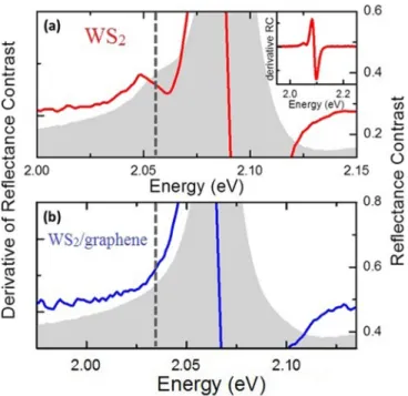
FIG. 2. Trion feature of the A exciton in the reflectance contrast spectrum of bare WS
2and of the WS
2/graphene heterostructure, as measured at 70 K. (a) For bare WS
2, the (energy) derivative of the reflectance contrast spectrum is shown as a red line. The gray shading (right vertical scale) is the reflection contrast spectrum itself.
The derivative of the reflectance contrast is plotted over a larger energy range in the inset. The position of the trion is indicated by a vertical dashed line. (b) The same data is plotted for a WS
2/graphene heterostructure. In this case, there is no signature of the trion absorption.
absorption of graphene. However, the heterostructure spectrum is not simply the sum of the isolated WS 2 and graphene absorption spectra. To demonstrate this, we plot in the bottom half of Fig. 1 the summed graphene and WS 2 spectrum compared to the measured heterostructure spectrum. We note two major differences: the measured exciton peaks in the heterostructure are broadened and redshifted. The bottom inset of Fig. 1 shows a redshifted, summed spectrum to allow a more direct comparison of the width of the A exciton peaks. We attribute the redshift to screening by the dielectric environment associated with the graphene. The relatively modest observed shift in the exciton transition energy reflects the combination of a significant renormalization of the quasiparticle band gap, offset by a decrease in the exciton binding energy [58].
In Fig. 2, we present reflectance contrast spectra for the sample at a temperature of approximately 70 K. In each panel we also show the spectrum’s derivative, with respect to energy, to bring out weak features. As is typical for exfoliated samples on a substrate [27], a trion feature appears in the reflectance contrast of bare WS 2 due to unintentional doping of the sample. The corresponding peak position is about 2.05 eV, on the low-energy shoulder of the neutral A exciton. When WS 2 is capped with graphene, as shown in Fig. 2(b), the trion feature disappears. The absence of a trion feature for the WS 2 /graphene heterostructure is not unexpected, since, upon contact, residual charges in the WS 2
could flow into lower-energy states via static charge transfer
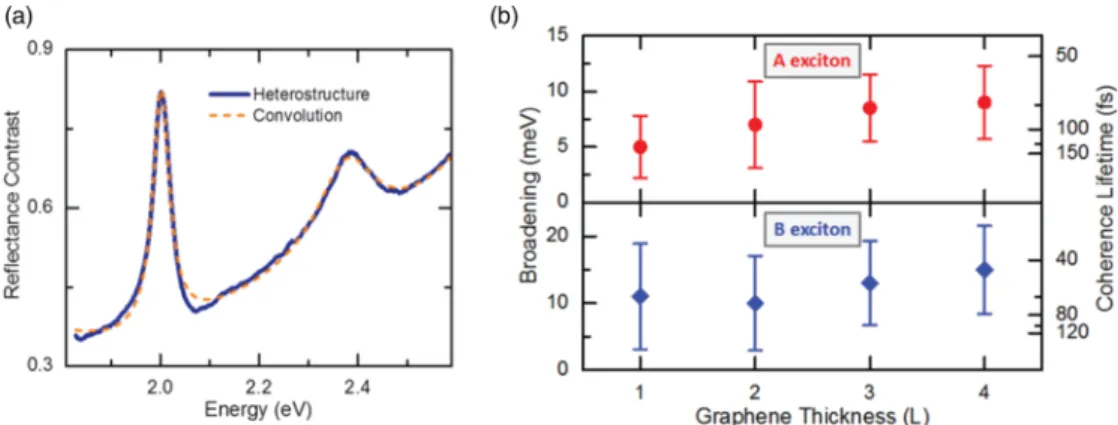
FIG. 3. (a) The room temperature reflectance contrast of a heterostructure is shown as well as the convolution of the sum of the individually measured constituent layers’ spectra with a Lorentzian profile. The blue curve is the experimental reflectance contrast data from the heterostructure shown in Fig. 1. The dashed orange curve comes from convoluting the sum of the graphene and bare WS
2reflectance contrast with a Lorentzian profile of 7 meV. (b) Linewidth broadening and coherence lifetimes for the A and B exciton of WS
2in the heterostructure are presented as a function of the thickness of the graphene; the data were taken at room temperature. The top and bottom halves of the graph show the broadening of the A and B exciton peaks in the reflectance contrast, respectively. The thickness of the graphene is given in terms of layer numbers (L). Coherence lifetimes are obtained from the relation τ = h/, accompanied by error bars associated ¯ with the extracted broadening uncertainty. The experimental range of lifetimes extracted with convolutions is 65 fs–130 fs, compared with the 55 fs–100 fs lifetime range extracted with the individual Lorentzian peak fitting, which assumes an ideal system and thus provides an even lower, yet theoretical bound to the lifetimes.
in the semimetallic graphene layer, whose Fermi energy is located in the gap of the WS 2 . The evidence of static charge transfer to graphene, coupled with the Raman spectroscopy data provided in Sec. 6 of the Supplemental Material [60], will assist us in our overall interpretation of the exciton broadening in the discussion section.
To analyze the exciton line broadening more precisely, we try to replicate the heterostructure experimental data by starting with summed and redshifted WS 2 and graphene spectra for the isolated layers and then convolving this spectrum for noninteracting layers with a Lorentzian line shape. The width of the Lorentzian is separately optimized for the A and B exciton features. Alternatively, we can simply fit each exciton feature in the isolated WS 2 to a Lorentzian peak and compare this width to that obtained in a similar fashion for the heterostructure. The latter procedure gives a broadening several meV less than the former but assumes negligible inhomogeneous broadening in the fitting process.
The convolution method does not require any particular assumptions with respect to the underlying peak structure and line shape, since the spectra include both minor features from excited exciton states, as well as the broad shoulder from higher energy resonances, such as the C feature.
In Fig. 3(a), we compare the experimental reflectance contrast spectrum of the A exciton of the heterostructure with the reflectance contrast spectrum for noninteracting layers (i.e., taking the sum of the measured spectra of bare WS 2 and bare graphene). The latter spectrum was then convoluted with a Lorentzian peak to simulate the broadening we observe in the heterostructure’s experimental data. The Lorentzian width, given by , in the convolution integral provides an upper bound for the observed increase in homogeneous linewidth.
If this broadening arises from a new decay channel for WS 2 excitons due to the presence of graphene, we then have a lower bound for the observed lifetime of this process, given by τ = h/. ¯
The broadening values and associated lifetimes for the A and B exciton transitions are shown in Fig. 3(b) as a function of the thickness of the graphene that is placed on top of the WS 2 . We see that, within experimental uncertainty, the broadening does not have a strong dependence on graphene thickness up to tetralayer graphene and ranges between 5 and 10 meV. Overall, the broadening is 4–5 times less than that seen in TMDC/TMDC heterostructures [42,51,61], which was attributed to interlayer (i.e., not static) charge transfer.
IV. DISCUSSION A. Phonon broadening and doping
We now discuss possible physical mechanisms leading to the exciton line broadening in the WS 2 /graphene heterostruc- ture. Several possible mechanisms can be identified, including enhanced phonon broadening in the heterostructure, changes in doping, and scattering within or between layers, including charge transfer and energy-transfer processes. The mention of charge transfer in the following arguments is not a reference to the distinct static charges moving from WS 2 to graphene upon the layers making initial contact. We proceed to argue that the dominant processes to consider are indeed the latter two phenomena: energy and charge transfer of photoexcited carriers from WS 2 to graphene.
At room temperature, the A exciton peak in a typical
exfoliated monolayer WS 2 has a width of about 40 ( ± 10) meV,
as in our samples. As indicated by temperature-resolved
measurements and theoretical modeling [62,63], about 20 meV
of this linewidth primarily arises from exciton scattering
with thermally activated phonons and a small contribution
from the radiative recombination on the order of several
meV. When the WS 2 flake is in contact with graphene, we
could in principle expect to see increased phonon scattering
from interaction of excitons in WS 2 with the phonons in
the graphene layer. However, this additional scattering is
unlikely given the expected inefficiency of such a process due to the small extension of the exciton wave function in the out-of-plane direction. That is further supported by the observation of similar broadening of the exciton linewidth at low temperatures, where the exciton-phonon-scattering contribution already in the WS 2 layer is on the order of only a few meV [63]. While the width of the excitonic features changes quite dramatically (the 70-K temperature spectrum is available in the Supplemental Material [60]), the broadening does not change to within 1 meV. This also implies that the processes giving rise to the broadening do not strongly depend on the temperature, unlike what we would expect for an additional exciton-phonon scattering channel.
As previously discussed in Fig. 2, the trion feature, seen clearly in the low-energy shoulder of the A exciton in the WS 2 spectrum, has undergone a strong reduction in the heterostructure spectrum. The bare WS 2 spectrum indicates doping on the order of 3 × 10 12 cm −2 , as extracted from the trion-exciton separation energy [64], typical for exfoliated samples on substrates. The heterostructure spectrum, however, has no obvious trion feature, strongly suggesting that the doping conditions across the WS 2 sample in contact with graphene are close to charge neutrality due to the expected transfer of the static charge to graphene. A change in the initial doping of a sample can change the width of the excitonic features in the reflectance contrast. However, typically a reduction in the doping would cause the peaks to become narrower, as previously observed in WS 2 monolayers [64].
In this case, a dedoping of a maximum carrier density of 3 × 10 12 cm − 2 would correspond to a linewidth narrowing of about 3 meV, in contrast to the observed increase of the linewidth [64]. Therefore, the change in doping cannot be considered as the cause of the observed broadening and may even lead to an overall underestimation of the extracted values for the broadening by a few meV.
B. Intervalley scattering as a source of broadening In our system, the arbitrary angle between the layers and the general reconfiguration of the WS 2 band structure in the heterostructure may introduce intervalley scattering within the WS 2 layer as another possible broadening mechanism which comes from two potential sources. The first source would be from changes to the band structure of WS 2 such that it exhibits an indirect band gap at the Q or point. The second source would be from the potential overlap or hybridization of electronic states from WS 2 with those in graphene at various parts of the Brillouin zone (BZ), perhaps at the K point in the case of resonant tunneling.
In MoS 2 , the difference between the valence-band energy of and K in the unperturbed, direct gap case, is 0.1 eV for monolayer MoS 2 , but there is a 0.3-eV maximum shift due to the presence of graphene [65]. In the case of WS 2 /graphene heterostructures, the -point maximum is 0.3 eV below that of the K point from angle-resolved photoemission spectroscopy (ARPES) [66]. MoS 2 /graphene heterostructures have been reported to form an indirect gap at the point (with a difference less than 0.2 eV with the K point) [36], but other literature suggests that MoS 2 /graphene retains its direct band gap [66].
Therefore, if the graphene layer causes a similar change in the
WS 2 , it is unlikely that WS 2 forms an indirect band gap. In the second case, ARPES measurements suggest that there is no significant overlap of electronic states at the K, Q, or point between graphene and WS 2 [66–68]. We will revisit this second case in the charge-transfer discussion.
The remaining two significant processes to consider are charge and energy transfer. The fastest time scales for either charge transfer or energy transfer to occur in this system is on the order of 100 fs, as extracted from the experimental linewidth broadening. If we compare our system to other low-dimensional systems, we can approximate the contribution from nonradiative energy transfer via near-field dipole-dipole interactions. For example, the energy-transfer rate from nanoparticles and nanoplatelets to graphene has been reported to be around 1 ns, where the distance from the emitter to graphene is on the order of a few nanometers [69–71].
Federspiel et al. experimentally observed a d −3 dependence for the energy-transfer rate between two-dimensional (2D) CdSe nanoplatelets and graphene [72]. Hernández-Martínez et al.
calculate a d − 4 energy-transfer rate between general 2D-2D interfaces [73], though at short length scales, the scaling deviates from this form when taking into account the nonlocal effects for graphene that become prominent at distances below 1 nm [57,73]. Gaudreau et al. also predict a similar enhancement in rates as a function of the distance to graphene [74]. We use both of these distance dependencies to obtain a range of expected energy-transfer rates. The separation between the donor and acceptor in our system is 0.5 nm from atomic force microscopy measurements (see Supplemental Material [60]). If we scale the 1-ns rate mentioned above, we obtain an expected rate for our system of 3 ps to 0.2 ps or a broadening of 0.2 meV to 2 meV. Furthermore, the enhanced oscillator strength for WS 2 in Ref. [27] compared to the platelets should further increase the rate of energy transfer and resultant broadening of the exciton line [75]. It is therefore conceivable that energy transfer contributes to the observed exciton broadening.
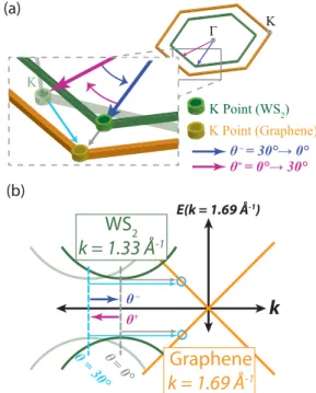
Concerning charge transfer, reported rates fall into a similar range for rare-gas adlayers on metal surfaces and similar systems (10–100 fs) [76,77]. Recent literature reports charge-transfer rates of tens of femtoseconds in TMDC/TMDC heterostructures [51,62]. Based on the previous discussion about treating the WS 2 /graphene heterostructures as having a direct band gap, one must question whether charge can transfer from the K point of WS 2 into graphene directly or if it requires a phonon-assisted process, which is set to occur for phonon energies as low as 84 meV, based on the alignment parameters in Ref. [59]. To elaborate, since the basic reciprocal lattice parameters in WS 2 and graphene are 1.33 ˚ A −1 and 1.69 ˚ A −1 , respectively, 0.36 ˚ A −1 is the absolute momentum difference between the two K points only in the case where both materials are aligned. In this zero-degree orientation, one can depict the two materials’ dispersions, as in Fig. 4, to see that a phonon is required to impart at least 0.36 ˚ A − 1 of additional momentum, which is equivalent to 84 meV assuming the effective mass of the charge is 0.16m 0
[27], to transfer charge from WS 2 to graphene. Since various
Raman modes exist in WS 2 , such as the E 1 2g () and A 1g (),
with respective energies of approximately 44 and 52 meV and
Graphene k = 1.69 Å -1
E(k = 1.69 Å
-1)
k
K Point (WS
2)
(b)
(a) K
K
K Point (Graphene)
+ –
+ –