Charge and current responses of spin-orbit coupled two-dimensional materials
DISSERTATION ZUR ERLANGUNG DES DOKTORGRADES DER NATURWISSENSCHAFTEN (DR. RER. NAT.) DER FAKULT ¨AT F ¨UR
PHYSIK DER UNIVERSIT ¨AT REGENSBURG
vorgelegt von Andreas Scholz
aus Regensburg
im
Jahr 2013
Promotionsgesuch eingereicht am: 16.10.2013
Das Promotionskolloquium fand statt am: 19.12.2013 Pr¨ufungsausschuss:
Vorsitzender: Prof. Dr. John Lupton 1. Gutachter: Prof. Dr. John Schliemann 2. Gutachter: Prof. Dr. Klaus Richter weiterer Pr¨ufer: Prof. Dr. Gunnar Bali
Contents
List of abbreviations 5
1. Introduction 7
2. Single-particle properties of graphene, monolayer MoS2, and p-doped III-V
semiconductors 13
2.1. Graphene . . . 13
2.2. Monolayer MoS2 . . . 19
2.3. Luttinger’s Hamiltonian for p-doped III-V semiconductors . . . . 22
3. The dielectric function in Random Phase Approximation 29 3.1. Theory of linear response . . . 30
3.2. Dielectric function . . . 34
4. Dielectric function, plasmons, and screening of graphene in the presence of spin-orbit interactions 39 4.1. The model . . . 40
4.2. Analytical results for the free polarizability . . . 41
4.3. Collective charge excitations . . . 45
4.4. Screening of impurities . . . 47
4.5. Summary . . . 50
5. Dynamical current-current susceptibility of gapped graphene 53 5.1. The model . . . 54
5.2. Analytical results for the current-current susceptibility . . . 55
5.3. Static limit and magnetic susceptibility . . . 57
5.4. Nonrelativistic limit of gapped graphene . . . 60
5.5. Summary . . . 62
6. Plasmons and screening in a monolayer of MoS2 65 6.1. The model . . . 66
6.2. Collective charge excitations . . . 68
6.3. Screening of impurities . . . 71
6.4. Summary . . . 73
7. Plasmons in spin-orbit coupled two-dimensional hole gas systems 75 7.1. The model . . . 76
7.2. Subband dispersion and density of states . . . 78
8. Interplay between spin-orbit interactions and a time-dependent electromagnetic
field in graphene 85
8.1. The model . . . 86
8.2. Energy spectrum and density of states . . . 89
8.3. Spin polarization and wave packet dynamics . . . 95
8.4. Optical conductivity . . . 98
8.5. Summary . . . 101
9. Conclusions 103 A. Details on the calculation of the free polarizability of graphene 107 A.1. Zero doping . . . 107
A.2. Finite doping . . . 110
B. Details on the calculation of the current susceptibility of graphene 115 B.1. Imaginary part . . . 116
B.2. Real part . . . 117
List of abbreviations
2D Two-dimensional
2DEG Two-dimensional electron gas BZ Brillouin zone
DF Dielectric function DOS Density of states
EHC Electron-hole continuum ELF Energy loss function
HREELS High-resolution electron-energy-loss spectroscope KMM Kane-Mele model
ML-MDS Monolayer molybdenum disulfide OMS Orbital magnetic susceptibility
QW Quantum well
RPA Random Phase Approximation SOC Spin-orbit coupling
SOI Spin-orbit interaction
TB Tight-binding
TBZ Time Brillouin zone
THz Terahertz
1
Chapter 1.Introduction
Carbon, one of the lightest elements and a cornerstone of the existence of living beings, has awaken gorgeous hopes among material scientists in the recent decades. Although its two most prominent allotropes, graphite and diamond, have been well-known for hundreds of years, the current interest in carbon-based nanostructures mainly began due to three se- quential discoveries: In the 1970s theoretical investigations of Eiji Osawa [1] predicted the stability of large molecules solely made of carbon. These molecules, known as fullerenes, were eventually discovered in 1985 [2] by Robert Curl, Harold Kroto, and Richard Smalley, earning them the Nobel Prize in Chemistry in the year 1996 [3]. Apart from established applications in anti-aging products, the fullerenes are traded as compounds of future semi- and superconducting materials, as catalysts in chemical reactions, and for medical pur- poses [4]. Only a few years after the experimental proof of the fullerenes succeeded, a serendipity in an electron microscope again demonstrated carbon’s manifold appearances after few layers of graphite, wrapped up cylindrically to form so-called carbon nanotubes, were discovered in the early 1990s [5]. The new research field based on carbon nanotubes offers a variety of possible applications such as transistors, energy storages, and as sub- stitutes for heavier materials [6]. Having seen manifestations of carbon in three (graphite and diamond), one (carbon nanotubes), and zero dimensions (fullerenes), it is natural to ask for a stable two-dimensional (2D) configuration. Unfortunately, early theoretical investigations gave a very disappointing answer regarding the crystallographic long-range order in two dimensions, and hence 2D (carbon) lattices were expected not to exist [7, 8].
In fact, until 2004 2D solids were mainly studied in quantum well (QW) heterostruc- tures such as GaAs/GaAlAs compounds, where the charge carrier movement is confined along one direction. This changed in 2004 when the research group of Andre Geim and Konstantin Novoselov isolated, detected, and gated a monolayer of graphite known as graphene for the first time [9]. Although single sheets of graphite had already been re- ported by Hanns-Peter Boehm in 1962 [10], compared to the mechanical exfoliation method of Geim and Novoselov the reduction of graphite oxide used in Boehm’s experiments di- minished some of the special characteristics of graphene [11]. Moreover, gating the flake was a subtle point to demonstrate that graphene is a fascinating material not only because of its dimensionality, but also due to its outstanding electrical, mechanical, and optical properties; see Refs. [12, 13] for an overview. As a consequence, the zero-gap semiconduc-
tor graphene with its characteristic linear bands at low energies [14] soon attracted a huge amount of interest in the scientific community due to fundamental questions (‘quantum electrodynamics in a pencil trace’ [15]), and because of a variety of possible applications [13, 15]. The significance of graphene was even underlined in 2010 when the Nobel Prize of Physics was awarded to Geim and Novoselov ‘for groundbreaking experiments regard- ing the two-dimensional material graphene’ [16]. Even nine years after the marvelous experiments of Geim and coworkers, graphene remains one of the most intensively studied materials and an enormous interest still exists in this remarkable carbon-based structure, as evident by the recent funding of the Graphene Flagship by the European Union which allocated one billion euro for the next ten years to support scientists working in various research fields of graphene [17].
Since the birth of graphene in 2004 a hunt on other truly 2D materials with prominent characteristics has begun. It has been demonstrated that single sheets of boron nitride [18], molybdenum disulfide [18, 19], and silicon [20, 21] can be isolated and it is very likely that others will follow as time goes by. Moreover, some of the properties of graphene are not set in stone, but they can rather be modified by chemical manipulation. The two most prominent examples are graphane [22, 23, 24] and fluorographene [25, 26]. In the former the carbon atoms are bound to hydrogen atoms which leads to a remarkable band gap opening (of the order of electron Volt), while in the latter fluorine atoms induce a finite magnetization in the sample.
Among the many peculiarities of graphene [12, 13, 15] are the high carrier mobility, allowing quantum Hall measurements even at room temperature, the low resistivity, mak- ing graphene potentially useful as a substitute of silicon in transistors, the very large in-plane stiffness leading to relatively high phonon energies [27], and the high absorp- tion rate of 2.3% per layer [28]. Apart from a variety of possible applications such as transistors, solar cells, sensors, or displays, graphene recently came in the focus of plas- monics [29, 30, 31, 32, 33, 34, 35, 36], where density waves created by an incident light beam carry optical signals through a nanostructure. Compared to the surface plasmons in metals, graphene offers a number of striking advantages:
(i) The measured plasmon wavelengths of about 250 nm are very short and in particular roughly 40 times smaller than the wavelength of the laser source [31, 32, 33], which in turn leads to a high localization of the electric field.
(ii) The optical absorption at the plasmon resonance is about one order of magnitude larger than in metals, hence dropping the requirement of having low temperatures in experiments [31].
(iii) The Fermi energy and thus the plasmon wavelength in graphene is widely tunable by means of an electric gate voltage [31, 32, 33]. As very large carrier concentrations up to values of 1014 cm−2 have been reported in the literature [35], this allows wavelengths ranging from the terahertz (THz) to the visible regime.
(iv) It was demonstrated that the damping rate of the plasmons in graphene can be enhanced by approaching the charge neutrality point, allowing to switch on/off the plasmon propagation depending on the Fermi energy [32].
9 In order to understand the dynamics of the collective charge excitations in graphene and related materials, a detailed analysis of the dynamical dielectric function (DF), or equiv- alently of the conductivity is indispensable. The DF is relevant not only in view of plas- monics, but also for the transport characteristics, the screening behavior of the Coulomb potential of charged particles, and the phonon spectra. Moreover, the interaction between electrons and plasmons leads to bound states known as plasmarons [37], which have been observed previously in graphene [38, 39].
The aim of the present work is to give a detailed study of the single- and many-particle properties of three different 2D materials: graphene, a monolayer of molybdenum disul- fide (ML-MDS), and p-doped III-V semiconductor QWs. As a generalization of previous works we explicitly take into account the effect of the various types of spin-orbit interac- tions (SOIs). While SOIs in graphene were initially considered as being negligible [40], recent experimental and theoretical works have demonstrated that spin-orbit coupling (SOC) might be relevant in graphene as the characteristic parameters can be enlarged significantly by changing the environment of the sample [41, 42, 43, 44, 45]. Moreover, the discussion of SOIs in graphene deserves attention also in view of other honeycomb lattices with similar properties such as silicene [46, 47] or ML-MDS [48]. The latter is considered as a possible alternative to graphene and as an auspicious candidate for valley- [49, 50, 51]
and spintronics [52] due to the distinct band gap of about 1.82 eV, the large intrinsic SOC of 80 meV [53, 54, 55], and the lack of a center of inversion. On the other hand, quantum well structures provide a fertile ground to investigate the effects of SOIs on the plasmon spectrum due to their inherently large SOIs [56] and because of the established controllability of the Rashba SOC by means of external electric fields [57].
This thesis is organized in the following way: In Chap. 2 we introduce the low-energy description of graphene, ML-MDS, andp-doped III-V semiconductors and discuss the in- fluence of the different types of SOIs on the single-particle properties.
Chapter 3 summarizes the formalism of linear response and introduces the Kubo sus- ceptibility as the central transport quantity. We describe how the Random Phase Ap- proximation (RPA) applied to the charge and current responses can be used to extract information on the collective charge excitations of the system and briefly comment on recent measurements of the plasmon energies in graphene by means of energy loss spec- troscopy [58, 59].
In Chapter 4 we study the dielectric properties of graphene in the presence of SOIs of the intrinsic and Rashba type. The main result of this chapter consists in the derivation of closed analytical expressions for the DF in RPA for arbitrary frequency, wave vector, doping, and SOC parameters. We show how SOIs in graphene might be used to change the plasmon energy and lifetime, which in turn might be interesting in view of plasmonics.
For a sufficiently large Rashba SOC the system exhibits a new plasmon mode with an energy much larger than those of the long-wavelength result. However, this mode always lies in the region where the creation of electron-hole pairs is permitted and thus has a finite lifetime. From the static limit of the DF the asymptotic behavior of the screened Coulomb potential of a charged impurity is investigated. Away from the charge neutrality point the Coulomb potential exhibits characteristic Friedel oscillations due to the existence of a sharp Fermi surface. In case the spin degeneracy of the bands gets lifted due to the
Rashba SOC, a beating of the Friedel oscillations is predicted.
After discussing the effect of an external charge density we analyze the current response of graphene in Chap. 5. Restricting ourselves in this chapter to the intrinsic SOC, we present analytical results for the transversal and longitudinal parts of the current-current susceptibility for arbitrary frequency, wave vector, and doping. The static limit of the current-current susceptibility allows to derive the orbital and Pauli part of the magnetic susceptibility. The orbital part for undoped graphene is shown to be proportional to the inverse of the SOC strength and in particular diverges for vanishing SOIs. By taking the nonrelativistic limit of gapped graphene, i.e., the limit of a band gap parameter compara- ble to the Fermi energy, we reproduce the results of an ordinary 2D electron gas (2DEG), but with a pseudospin Zeeman term due to the existence of a pseudospin degree of freedom [60]. The nonrelativistic limit is not of purely academic interest, but is closely related to other honeycomb structures with a large band gap in the energy spectrum such as ML- MDS.
This brings us to Chap. 6 where a numerical discussion of the dynamical DF of ML- MDS within the RPA is carried out. While in graphene damping of plasmons is caused by interband transitions [61, 62], due to the large direct band gap in ML-MDS, collec- tive charge excitations enter the intraband electron-hole continuum (EHC) similar to the situation in 2DEGs [63]. The carrier density dependence of the plasmon frequency in ML- MDS, ωq ∝ n1/2, turns out to be quite different compared to graphene where ωq ∝n1/4 [62]. Since there is no electron-hole symmetry in ML-MDS, the plasmon energies in p- and n-doped samples clearly differ. Moreover, the breaking of spin degeneracy caused by the large intrinsic SOI leads to a beating of Friedel oscillations for sufficiently high carrier concentrations.
In Chap. 7 we proceed with an investigation of the plasmon spectrum in quasi 2D hole gases, exemplified on GaAs and InAs QWs grown in the [001] direction. In our analysis we explicitly account for SOIs of the Dresselhaus and Rashba type. It is shown that the plasmon dispersion exhibits a pronounced anisotropy being much larger in GaAs compared to InAs. In GaAs this leads to a suppression of plasmons due to Landau damping in some orientations, while others are undamped. Due to the large Rashba contribution in InAs, the lifetime of plasmons can be controlled by changing the magnitude of an electric field.
This effect is potentially useful in a plasmon transistor as previously proposed for 2DEGs [64, 65].
The influence of a strong circularly and linearly polarized THz field on a monolayer of graphene is the subject of Chap. 8. As the field drives the sample out of equilibrium, distinct changes in the single-particle properties are expected. It turns out to be possible to induce a gap in the energy spectrum [66, 67] and to close an existing gap by using circu- larly polarized light. On the other hand, the spectrum becomes strongly anisotropic if the incident light is linearly polarized. We show that the time evolution of the spin polariza- tion and the orbital dynamics of an initial wave packet can be modulated by varying the ratio of the intrinsic and Rashba SOC parameters. Assuming that the system acquires a quasistationary state, the optical conductivity of the irradiated sample is calculated. It is shown that the THz field induces additional steps in the conductivity as reported recently in Ref. [68]. The number of steps in turn depends on the field amplitude and orientation,
11 as well as on the SOC parameters.
A conclusion of the main results of this thesis, together with a brief outlook on possible extensions can be found in Chap. 9.
In appendices A and B we provide details on the analytical calculations of the free polarizability and transversal part of the current-current susceptibility of graphene.
2
Chapter 2.Single-particle properties of graphene, monolayer MoS 2 , and p-doped III-V semiconductors
In the present chapter we introduce the effective low-energy description of graphene, ML- MDS, andp-doped III-V semiconductors such as GaAs or InAs. The respective Hamilto- nians form the starting point for the following chapters, where many-body effects in the dynamical charge and current susceptibilities are investigated.
We start with a tight-binding (TB) description of graphene in Sec. 2.1.1, where the basic steps to derive an effective Hamiltonian within a single-orbital model are summarized. In Sec. 2.1.2 this model is extended to include the effect of SOIs of the intrinsic and Rashba type within the Kane-Mele model (KMM). As SOIs in graphene are naturally very small, we discuss recent experimental progress and theoretical proposals to enlarge the energy scales of the SOC strengths.
Sec. 2.2 is devoted to ML-MDS, another honeycomb lattice made of sulfur and molyb- denum atoms instead of carbon. By comparing the effective two-band Hamiltonian of ML-MDS with that of graphene, we point out formal similarities and quantitative differ- ences. Based on recent results obtained from combinedab initio and TB studies, a short discussion of the validity of the two-band model is given.
Finally, in Sec. 2.3 we sketch the derivation of an appropriate model to explain the dynamics of holes in III-V semiconductors, including SOIs arising from bulk and structure inversion asymmetry. We describe how Luttinger’s model needs to be extended in order to properly account for a spatial confinement in a quasi 2D QW.
2.1. Graphene
2.1.1. Neglecting spin-orbit interactions
In Fig. 2.1(a) we show the graphene lattice in real space [12, 14, 69]. The lattice can be decomposed into two triangular sublattices, where an atom in sublattice A (B) has three nearest-neighbor carbon atoms located in sublattice B (A). The distance between neighboring atoms is aC−C ≈ 1.42 ˚A [12, 14, 69]. The lattice vectors of length a =
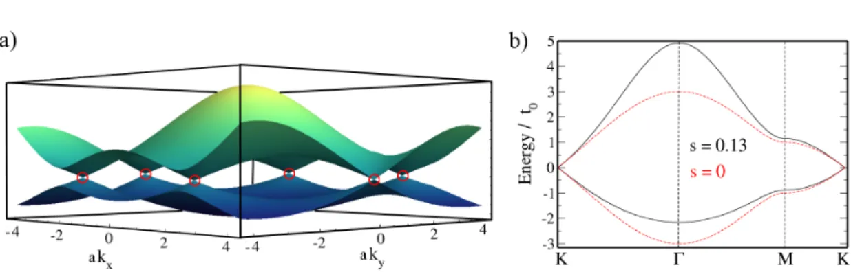
Figure 2.1.:(a) Real space lattice including unit cell (shaded region) and (b) first Brillouin zone of graphene.
√3aC−C ≈2.46 ˚A are chosen as
a1 = a 2
√1 3
!
and a2= a 2
−1√ 3
!
. (2.1)
Within this work all vectors have to be understood as 2D objects in the x-y plane, i.e., the plane where the charge carriers can freely move. Moreover, we set ~= 1 throughout the thesis. From
ai·bj = 2πδij, (2.2)
where δij denotes the Kronecker delta, it follows that the reciprocal lattice in Fig. 2.1(b) is spanned by the vectors
b1 = 2π
√3a
√3 1
!
and b2= 2π
√3a
−√ 3 1
!
. (2.3)
Only two of the six corners of the Brillouin zone (BZ), e.g., Kτ = 4π
3a τ 0
!
, with τ =±1, (2.4)
are independent as the others can be obtained by adding a multiple of the reciprocal lattice vectors b1 and b2 to Kτ. In graphene these special points are usually denoted as Dirac points or valleys.
The energy spectrum of graphene has been known since 1947, when Philip Wallace solved the TB model of the hexagonal carbon lattice in order to obtain information on the band structure of graphite [14]. Within the TB approximation, the solution of the time- independent Schr¨odinger equation in the presence of a spatially periodic lattice potential
2.1. Graphene 15 V(r),
pˆ2 2m0
+V(r)
!
Ψg,T B(r,κ) =Eg,T B(κ)Ψg,T B(r,κ), (2.5) wherem0 is the bare electron mass, is written as a linear combination of atomic orbitals, centered around the position of the lattice atoms at
RnA1n2 = 1
3 +n1
a1+
1 3+n2
a2 (2.6)
and
RnB1n2 = 2
3+n1
a1+
2 3+n2
a2, (2.7)
with n1/2 being integers. Graphene is made of carbon atoms with an electronic configu- ration of
C: [He]2s22p2.
Three of the valence electrons hybridize in sp2 orbitals, localizing the atoms at their lat- tice positions, while the remaining delocalizedpz orbital mainly determines the transport properties of graphene. As the unit cell defined by the lattice vectorsa1/2 [shaded region in Fig. 2.1(a)] contains two carbon atoms, the solution of Eq. (2.5) is approximated by a superposition of atomic 2pz wave functions ξ2pz(r):
Ψg,T B(r,κ) = 1
√N X
ν=A,B
Cνeiκ·R00ν ξ2pz(r−R00ν ), (2.8) where N is the number of lattice sites. The eigensystem follows from the generalized eigenvalue problem [14, 69]
Hˆg,T B CA CB
!
=Eg,T B(κ) ˆSg,T B CA CB
!
. (2.9)
For the energies this leads to the secular equation
dethHˆg,T B−Eg,T B(κ) ˆSg,T Bi= 0. (2.10) Restricting ourselves to nearest-neighbor hopping, the transfer matrix
Hˆg,T B = 2pz −t0f(κ)
−t0f∗(κ) 2pz
!
(2.11)
Figure 2.2.:Energy dispersion of graphene (a) within the full BZ and (b) along the high symmetry points.
and overlap integral matrix
Sˆg,T B= 1 sf(κ)
sf∗(κ) 1
!
(2.12) contain the on-site energy of the pz orbitals2pz, the function
f(κ) = 1 +eiκ·a1+eiκ·a2, (2.13) where geometric information of the lattice structure is included, and the nearest-neighbor hopping energy t0 and overlap integral s. For details on the derivation of the matrix elements of ˆHg,T B and ˆSg,T B we refer to Refs. [12, 14, 69], where intermediate steps of the calculation can be found. Solving Eq. (2.10), we obtain for the energies
Eg,T B,±(κ) = 2pz ±t0|f(κ)|
1∓s|f(κ)| . (2.14)
The TB parameters can be determined by comparison with ab initio calculations or ex- perimental data, which in turn gives values of t0 ≈ 3 eV and s ≈ 0.13 [12, 69]. The band structure of graphene is shown in Figs. 2.2(a) within the full BZ and (b) along the high symmetry points. Right at the corners of the BZ [indicated by the red circles in Fig. 2.2(a)], the conduction and valence bands touch. For most experimentally relevant carrier densities, n . 1013 cm−2, the dispersion is properly described around the Dirac points and the above Hamiltonian can, up to linear order in momentum, be approximated by (k=Kτ +κ) [12]
Hˆg,0τ =vFk·σˆτ +2pz, with τ =±1. (2.15) Here, ˆστ = (τσˆx,σˆy) is the vector of Pauli matrices acting on pseudospin space and the Fermi velocity in graphene is defined as
vF =
√3at0
2 ≈106m/s. (2.16)
2.1. Graphene 17 Neglecting in the following the overlap integral [which in fact leads only to small changes around the Dirac points; see Fig. 2.2(b)] and choosing the energy reference such that 2pz = 0, the isotropic dispersion obtained from Eqs. (2.10) and (2.15),1
Eg,0,±(k) =±vFk, (2.17)
withk=|k|, is that of a particle with vanishing effective mass propagating with a constant group velocity vF.
2.1.2. The influence of spin-orbit interactions
Up to now we did not consider the interplay between the spin degree of freedom and the orbital dynamics. For the inclusion of SOIs one needs to add [56, 70]
Hˆso = 1 4m20c2
"
∇V(r, z)× pˆ pˆz
!#
· ˆs sˆz
!
(2.18) to the Schr¨odinger equation in Eq. (2.5). Here,c denotes the speed of light and ˆsx,sˆy,ˆsz
the Pauli matrices in real spin space. The SOC term Eq. (2.18) can be deduced by taking the nonrelativistic limit of the Dirac Hamiltonian up to second order in the inverse of the rest energym0c2 [56, 70].
In the seminal work of Kane and Mele [71] it has been shown that by treating ˆHso perturbatively with respect to ˆHg,0τ [72, 73], SOIs can be incorporated into the low-energy description of graphene by adding the intrinsic
Hˆg,Iτ =τ λIσˆzˆsz (2.19) and extrinsic (Rashba) contribution
Hˆg,Rτ =λR(τσˆxsˆy−σˆysˆx) (2.20) to Eq. (2.15). The resulting Hamiltonian
Hˆgτ =vFk·σˆτ +τ λIσˆzsˆz+λR(τσˆxsˆy−σˆysˆx) (2.21) is known as the Kane-Mele model of topological insulators. While the intrinsic part is always present, the Rashba SOC arises if structure inversion symmetry becomes broken.
This can be done experimentally by applying an external electric field perpendicular to the graphene plane, or by putting graphene on a substrate. The isotropic energies of the KMM,
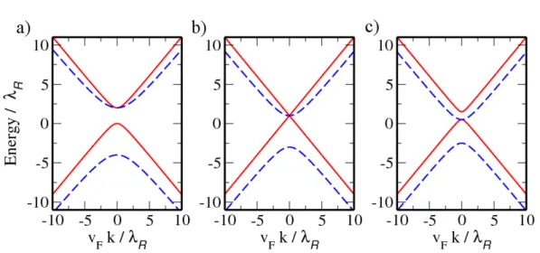
Eg,αβ(k) =α λR+β q
v2Fk2+ (λR−αλI)2, with α, β =±1, (2.22) are shown in Fig. 2.3 for three different combinations of the SOC parameters: λI = 2λR, λI =λR, and λI =λR/2. For λR 6= 0 the spin degeneracy of the bands is lifted and the
1Notice that the indexτ is missing in Eq. (2.17) as the energies are the same for both valleys.
Figure 2.3.: Energy dispersion of graphene for various combinations of the SOC parameters: (a) λI = 2λR, (b)λI =λR, and (c)λI =λR/2. The solid red lines are forE+±, the dashed blue lines forE−±.
Fermi contour consists of two concentric circles with radii given by kF±=
q
µ(µ∓2λR)±2λRλI−λ2I/vF. (2.23) For a sufficiently large intrinsic coupling parameter, λI > λR, the system exhibits a band gap in the bulk. If the sample becomes spatially confined along one direction, gapless edge states occur and the system is in the quantum spin Hall phase [71]. In the other case of λR> λI, the valence and conduction bands always touch at theK points and the system behaves as an ordinary semimetal. At the point where λR = λI, two of the four bands become linear and a threefold degeneracy occurs at the Dirac points.
Let us now discuss the importance of SOIs in typical graphene samples. As graphene is composed of relatively light (carbon) atoms,2 SOIs in graphene are expected to be small.
After some controversy regarding the actual values of the intrinsic and Rashba spin-orbit coefficients, ranging from 1µeV to 200µeV forλI[71, 72, 74], it was eventually found that the values are close toλI= 12µeV andλR= 5µeV for an electric field of 1 V/nm [40, 75].
In order to obtain these numbers it turned out to be necessary to also include thedorbitals as they give the dominant contribution toλI(roughly 95%) and to considerσ-π mixing for the Rashba coefficient. Due to the small values of λR and λI, in the beginning the focus of graphene research was mainly set on spin-independent phenomena. However, recent experimental and theoretical works have impressively demonstrated that SOC effects might be relevant as the characteristic parameters can be enlarged significantly by changing the environment of the sample [41, 42, 43, 44, 45]. As an example, we mention Ref. [44], where it was predicted that the intrinsic contribution can be enlarged up toλI ≈10 meV, i.e., by three orders of magnitude, if the system is doped with suitable adatoms such as thallium.
Alternatively, putting graphene on a Ni(111) surface, as described in the experiment of
2The atomic spin-orbit splitting of the carbon 2pz orbitals is about 8 meV [73].
2.2. Monolayer MoS2 19 Ref. [41], enhances the Rashba contribution to a remarkable value ofλR≈225 meV.3
Finally, we want to point out a formal similarity between the KMM and the low-energy Hamiltonian of bilayer graphene. Restricting ourselves to nearest-neighbor and interlayer hopping, i.e., neglecting higher order terms such as trigonal warping, bilayer graphene can be described by two monolayer graphene Hamiltonians, coupled by the interlayer hopping tIL≈0.38 eV [76]:
HˆBLGτ =
Hˆgτ 0 0 tIL 0 0 tIL
0 0 Hˆgτ
. (2.24)
The KMM in Eq. (2.21) with only Rashba SOC taken into account can now be mapped onto the bilayer Hamiltonian of Eq. (2.24), relating the interlayer constant to the Rashba coefficient via
±2iλR→tIL. (2.25)
While the energies of bilayer graphene equal that of Eq. (2.22) (with λI = 0), EBLG,αβ(k) = α tIL
2 +β s
vF2k2+ tIL
2 2
, with α, β=±1, (2.26) the eigenstates only differ by a unitary transformation. Therefore, some of our findings, such as the analytical solution of the free polarizability of graphene in the presence of a purely Rashba SOC discussed in Section 4, can also be applied to bilayer graphene.
2.2. Monolayer MoS
2As mentioned in the introductory chapter, another promising 2D material that has at- tracted a lot of attention in the last years is ML-MDS. In the unit cell the molybdenum atom in ML-MDS is arranged in-between two sulfur layers; see Fig. 2.4(a). In top view [Fig. 2.4(b)], both the ML-MDS lattice and BZ show the same hexagonal structure as graphene. However, the electronic configuration of the constituents,
S : [Ne]3s23p4 and Mo : [Kr]4d55s1,
and the spatial arrangement of the atoms (compared to graphene the lattice is strongly buckled) make the derivation of an adequate TB model much more complicated than in graphene. Moreover, as ML-MDS lacks inversion symmetry and due to the influence of thedorbitals of molybdenum, SOIs are generally expected to be important. As described
3It should be emphasized that these samples can no longer be considered as graphene, but rather as graphene-likeas the influence of the adatoms and charge transfer to the substrate cannot be neglected.
For the discussion in the following chapters, however, the term spin-orbit coupled graphene will be used for all kinds of materials that can effectively be described by the KMM model of Eq. (2.21), independently of the physical origin of the large SOC contributions.
Figure 2.4.: (a) Unit cell and (b) top view of the ML-MDS lattice.
in Ref. [54], a possible starting point is to construct the basis orbitals of the TB model by linear combinations of thedz2,dx2−y2, anddxy orbitals of molybdenum, and thepxandpy
orbitals of sulfur, where for each spin component4 one ends up with a seven-dimensional TB Hamiltonian.
As in graphene, the valence (conduction) band maxima (minima) in ML-MDS appear at the corners of the BZ, where low-energy transport will be most important. Around the K points, the seven band TB Hamiltonian can further be reduced to an effective two-band model by means of L¨owdin partitioning [54, 55]:
Hˆmτ s =∆
2ˆσz+τ sλI
1−σˆz
2 +t0a0k·σˆτ
+ k2 4m0
(α+βσˆz) +t1a20k·σˆ∗τˆσxk·σˆ∗τ, (2.27) where τ, s=±1 denote the valley and real spin components, respectively. The analytical solution of the energies obtained from Eq. (2.27),
Em,±τ s (k) = α
4m0k2+sτ λI
2 ±
(
a40t21+ β2 16m20
! k4+
∆−sτ λI 2
2
+k2
a20t20+β(∆−sτ λI) 4m0
+ 2τ t0t1a30k3cos (3φk) )1/2
, (2.28)
where tanφk = ky/kx is the in-plane angle, is shown in Fig. 2.5 for both valley and spin polarizations. Table 2.1 summarizes the band parameters of ML-MDS according to Ref. [54]. Due to the large value of the staggered potential ∆ = 1.9 eV, a distinct energy gap of 1.82 eV separates the valence and conduction bands. As Eq. (2.28) is not
4Notice that, as for graphene, spin remains a good quantum number even in the presence of intrinsic SOIs. This changes if additionally the Rashba contribution is considered. However, in the following we neglect the Rashba term in ML-MDS due its small effect on the energy spectrum.
2.2. Monolayer MoS2 21
t0 aM o−S θ a0 =aM o−Scosθ ∆ λI α β
1.68 eV 2.43 ˚A 40.7◦ 1.87 ˚A 1.9 eV 80 meV 0.43 2.21
Table 2.1.:Band parameters of ML-MDS. aM o−S is the length of the Mo-S bond andθ= 40.7◦ the angle between thex-yplane and the Mo-S bond; see Fig. 2.4. Values taken from Ref. [54].
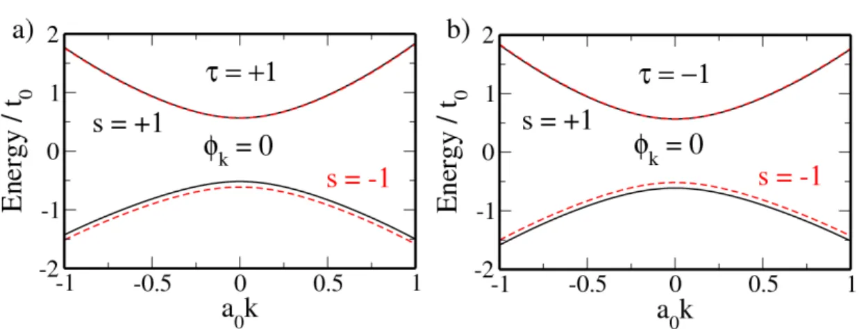
symmetric with respect to a sign change in λI, the intrinsic SOC furthermore lifts the spin degeneracy of the bands. While the valence band degeneracy is clearly lifted even atk= 0, the conduction bands remain degenerate at theK points, but differ slightly for larger momenta due to the different curvature of the bands; see Fig. 2.5. Because of time- reversal symmetry the corresponding shift in energy has to be opposite at the two valleys, where for τ = +1 (τ =−1) the s= +1 (s=−1) component is energetically higher. The trigonal warping term proportional tot1 causes the spectrum to be anisotropic. However, ast1 = 0.1 eV is small compared to the other energies, this anisotropy is weak and hence we plot only a single in-plane angle of φk = 0◦.
Having a closer look on the low-energy model of ML-MDS, we notice that the first line in Eq. (2.27) is essentially the Hamiltonian of gapped graphene (i.e., Eq. (2.21) withλI 6= 0 andλR= 0). Here, each contribution with valleyτ and spinsis described by an effective mass term given by
λ˜τ sI = ∆
2 −sτ λI
2 (2.29)
and a shifted Fermi energy of
µ˜τ s=µ−sτ λI
2 . (2.30)
In fact, in Ref. [53] the effective TB Hamiltonian of ML-MDS was found to be Hˆm,simpτ s = ∆
2σˆz+τ sλI
1−σˆz
2 +t0a0k·σˆτ. (2.31) However, it was pointed out later that Eq. (2.31) is not sufficient to properly describe recent ab initio data [54, 55], where different electron and hole masses were reported.
We should also mention that in Ref. [77] the band structures of ML-MDS and multilayer MoS2 were investigated within the full BZ; the resulting Hamiltonian turned out to be a further generalization of Eq. (2.27). One of the findings of Ref. [77] and of previous works [55, 78, 79] was that additional band extremes close to the K point minima and maxima might be relevant for transport. These additional bands, at the Γ point for holes and between the K and Γ point for electrons, are not taken into account in Eq. (2.27). For the carrier densities used in Chap. 6, n = 1012 cm−2 (comparable to the experiment in Ref. [80]) and 5·1013cm−2 (where both valence bands are filled in thep-doped case), we will neglect the influence of the higher bands since the additional extremes are expected to be important only for densities larger than 1014cm−2and the two-band model in Eq. (2.27) should give appropriate results [55, 79]. However, a detailed analysis of the effect of the full BZ on the charge response [81] is left open for future works.
Figure 2.5.: Energy spectrum of ML-MDS around theK points for (a) τ = +1 and (b)τ =−1 for the real spin component s = +1 (solid black) and s= −1 (dashed red). The in-plane angle tanφk =ky/kxwas set to φk= 0◦.
Let us finally comment on two further things: First of all, even though the models of graphene Eq. (2.21) and ML-MDS Eqs. (2.27) and (2.31), respectively, share several formal similarities, large quantitative differences appear. While the band gap in graphene (of a fewµeV) is naturally very small, the valence and conduction bands in ML-MDS are largely separated by 1.82 eV. Moreover, the intrinsic SOC term in ML-MDS is more than three orders of magnitude larger than that in graphene, resulting in a distinct spin splitting of the valence bands. Second, it is worth noticing that for an experimental realization of devices like transistors, the combination of various 2D materials can be used in order to tailor the band structure of a heterojunction according to our requirements. As an example, we mention Ref. [78], where ab initio calculations demonstrate the possibility to adjust the size of the band gap of a MoS2-WS2 bilayer compared to homogeneous compounds such as MoS2-MoS2or WS2-WS2, and even to transform the latter from indirect to direct band gap semiconductors.
2.3. Luttinger’s Hamiltonian for p-doped III-V semiconductors
Let us now turn to the single-particle description of holes in III-V semiconductors. In the following we restrict ourselves to GaAs and InAs as representatives, as both materials are commonly used in spintronic experiments [57]. Due to the relatively large Rashba SOC, InAs seems to be a promising candidate to manipulate the many-body properties of a QW by adjusting the SOC strength. In Chap. 7 we will discuss this point in view of the plasmon spectrum.
For an effective description of III-V semiconductors one could derive a suitable TB model similar to graphene or ML-MDS [82, 83]. However, for transport calculations (especially in view of an analytical treatment), it is often more convenient to describe the topmost valence bands by Luttinger’s model [56, 83, 84]. Due to Bloch’s theorem the analytical
2.3. Luttinger’s Hamiltonian forp-doped III-V semiconductors 23
Figure 2.6.: Schematic plot of the band structure of III-V semiconductors such as GaAs or InAs for the eight lowest conduction and six highest valence bands.
solution of Schr¨odinger’s equation with a spatially periodic potential is of the form5 Ψν(r, z;k, kz) =ei(k·r+kzz)uν(r, z;k, kz), (2.32) whereν is a set of quantum numbers anduν a lattice periodic wave function. As arsenic, gallium, and indium are relatively heavy atoms, the effect of SOIs, being proportional to the squared of the atomic number, has to be taken into account from the beginning.
Combining the Bloch wave function in Eq. (2.32) with Eqs. (2.5) and (2.18), we obtain a differential equation for uν:
ˆp2+ ˆp2z
2m0 +V(r, z) +k2+kz2
2m0 +k·pˆ+kzpˆz
m0 +
"
∇V(r, z)× pˆ pˆz
!#
· ˆs ˆsz
!
4m20c2
+
"
∇V(r, z)× k kz
!#
· sˆ sˆz
!
4m20c2
uν(r, z;k, kz) =Eν(k, kz)uν(r, z;k, kz). (2.33)
Usually, the crystal momentum |k|is small compared to the momentum of the holes |p|
(the expectation value of the momentum operator ˆp=−i∇) and we can neglect the last term on the left-hand side [56]. As the conduction band minima and valence band maxima in GaAs and InAs appear at the Γ point, we express the lattice periodic wave function for
5Notice that when we discuss III-V semiconductors in this section and in Chap. 7, the wave vectorkis measured with respect to the center of the BZ and not with respect to someK point.
finite wave vectors in terms of the Γ point solutions vα [56, 83]:
uν(r, z;k, kz) =X
α0
cνα0(k, kz)vα0(r, z). (2.34) Combining Eqs. (2.34) and (2.33) and projecting the result tov∗α, the expansion coefficients cνα and the corresponding energiesEν follow from the eigenvalue problem
X
α0
"
Eα0(0) + k2+k2z 2m0
!
δαα0 + 1 m0
k kz
!
· Pαα0 Pz,αα0
!
+ 1
4m20c2Σαα0
#
cνα0(k, kz)
=Eν(k, kz)cνα(k, kz). (2.35) Besides the usual kinetic part (k2+kz2)/2m0, Eq. (2.35) contains the band offsets Eα(0), and the off-diagonal momentum
Pαα0 Pz,αα0
!
= Z
d3r v∗α(r, z) ˆp pˆz
!
vα0(r, z) (2.36)
and SOC matrix elements Σαα0 =
Z
d3r vα∗(r, z)
"
∇V(r, z)× pˆ pˆz
!#
· ˆs sˆz
!
vα0(r, z). (2.37) By diagonalization of the matrix in Eq. (2.35), the energies and wave functions can be obtained for arbitrary wave vectors. In order to allow further analytical or numerical progress, it is necessary to simplify Eq. (2.35) by taking into account only a limited amount of bands exactly, while the others are treated perturbatively. Within the extended Kane model [56, 85, 86], we restrict ourselves to the eight lowest conduction [Γ7c(two), Γ6c(two), and Γ8c (four)] and six highest valence bands [Γ7v (two) and Γ8v (four)]; see Fig. 2.6 for a schematic plot of the band structure. The corresponding Hamiltonian then reads [56]:
HˆeKM =
Hˆ8c8c Hˆ8c7c Hˆ8c6c Hˆ8c8v Hˆ8c7v
Hˆ7c8c Hˆ7c7c Hˆ7c6c Hˆ7c8v Hˆ7c7v Hˆ6c8c Hˆ6c7c Hˆ6c6c Hˆ6c8v Hˆ6c7v
Hˆ8v8c Hˆ8v7c Hˆ8v6c Hˆ8v8v Hˆ8v7v Hˆ7v8c Hˆ7v7c Hˆ7v6c Hˆ7v8v Hˆ7v7v
. (2.38)
Choosing the energy reference at the top of the valence band, in thep-doped case we can approximate the block-diagonal parts of the conduction bands by [85]
Hˆ6c6c= ˜E0 1 0 0 1
!
, Hˆ7c7c= ˜E00 1 0 0 1
!
, Hˆ8c8c=E˜00 + ˜∆00
1 0 0 0 0 1 0 0 0 0 1 0 0 0 0 1
,
(2.39)
2.3. Luttinger’s Hamiltonian forp-doped III-V semiconductors 25 γ1 γ2 γ3 Ck (eV˚A) b8v8v41 (eV˚A3) r418v8v (e˚A2) r E0 (meV)
GaAs 6.85 2.10 2.90 -0.0034 -81.93 -14.62 12.5 6.4
InAs 20.40 8.30 9.10 -0.0112 -50.18 -159.9 14.6 19.3
Table 2.2.:Band structure and SOC parameters of GaAs and InAs. Values taken from Ref. [56].
r is the background dielectric constant (taken from Ref. [87]) and E0 = γ1π2/2m0d2 the size- quantization scale of ad= 20 nm thick QW (see Chap. 7).
and the valence bands by
Hˆ8v8v =−k2+k2z 2m0
1 0 0 0 0 1 0 0 0 0 1 0 0 0 0 1
, Hˆ7v7v =− k2+kz2 2m0 + ˜∆0
! 1 0 0 1
!
. (2.40)
The various energies ( ˜E0(0)and ˜∆(0)0 ) are defined in Fig. 2.6. If we now use L¨owdin’s method to decouple thep-like conduction bands Γ7cand Γ8c, and in a subsequent step do the same with the s-like Γ6c bands, we end up with a 6×6 Hamiltonian for the heavy hole, light hole, and split-off bands. Neglecting furthermore the effect of the mixing matrix elements between Γ8v and Γ7v, which in turn is a reasonable approximation in GaAs and InAs [56], one finally arrives at an Hamiltonian of the form [85]:
HˆV B =
HˆL,0 0 0 Hˆsp−o
!
. (2.41)
Here, ˆHsp−o describes the split-off bands (Γ7v) and ˆHL,0 is Luttinger’s Hamiltonian for the four topmost (Γ8v) valence bands. The influence of the conduction bands is taken into account in ˆHV B up to order 1/E˜0 in the fundamental gap. After carrying out the elongate steps of the calculation, as can be partly found in Refs. [56, 83], Luttinger’s model explicitly reads:
HˆL,0=− 1 2m0
γ1+5
2γ2
kx2+k2y+k2z−2γ2
kxJˆx+kyJˆy+kzJˆz
2
+γ3−γ2
m0
hkxkz
nJˆx,Jˆz
o+kykz
nJˆy,Jˆz
o+kxky
nJˆx,Jˆy
oi. (2.42)
Here {., .} is the anticommutator. The values for the Kohn-Luttinger parametersγ1,γ2, andγ3 in GaAs and InAs can be found in Table 2.2. The spin-3/2 matrices are defined as
Jˆx= 1 2
0 √
3 0 0
√
3 0 2 0
0 2 0 √
3
0 0 √
3 0
, Jˆy = 1 2
0 −i√
3 0 0
i√
3 0 −2i 0
0 2i 0 −i√
3
0 0 i√
3 0
,
(2.43)
and
Jˆz = 1 2
3 0 0 0
0 1 0 0
0 0 −1 0
0 0 0 −3
. (2.44)
Often ˆHL,0 is simplified by equating
γ2 =γ3 = ¯γ ≡ 2γ2+ 3γ3
5 . (2.45)
In this case the second line in Eq. (2.42) vanishes. The advantage of this (spherical) approximation is the relative simplicity of the energy spectrum. In three dimensions the subsequent twofold spin-degenerate bands then read
Eh/lsp(k, kz) =−k2+kz2
2mh/l , (2.46)
where
mh/l = m0
γ1∓2¯γ (2.47)
are the heavy and light hole masses. While the valence band energies in Eq. (2.46) resemble those of an ordinary electron gas, the corresponding eigenstates turn out to be clearly more complicated due to their nontrivial spin structure [88]. However, if the relative difference ofγ2 andγ3 is large, the anisotropic terms might be important and can lead to interesting physics. In Chap. 7 we will discuss this point further in context of the plasmon spectrum.
Apart from Luttinger’s Hamiltonian in Eq. (2.42), the extended Kane model features additional contributions in systems that lack a center of inversion. We distinguish between bulk inversion asymmetry, which is an intrinsic property and thus always present in zinc blende crystals, and structure inversion asymmetry, e.g., due to a suitably chosen electric field (E, Ez). In the former, Eq. (2.42) needs to be supplemented by the Dresselhaus term [89]
HˆD =2Ck
√ 3
hkxnJˆx,Jˆy2−Jˆz2o+kynJˆy,Jˆz2−Jˆx2o+kznJˆz,Jˆx2−Jˆy2oi +b8v8v41 hnkx, k2y−k2zoJˆx+nky, k2z−kx2oJˆy+nkz, k2x−ky2oJˆz
i
, (2.48) while the latter leads to the Rashba contribution [90]
HˆR=r418v8vh(kyEz−kzEy) ˆJx+ (kzEx−kxEz) ˆJy+ (kxEy−kyEx) ˆJz
i. (2.49)