Cubic Rashba Spin-Orbit Interaction of a Two-Dimensional Hole Gas in a Strained-Ge = SiGe Quantum Well
Rai Moriya,1,*Kentarou Sawano,2 Yusuke Hoshi,1,2,‡ Satoru Masubuchi,1,3Yasuhiro Shiraki,2 Andreas Wild,4,5 Christian Neumann,5 Gerhard Abstreiter,4,6 Dominique Bougeard,5 Takaaki Koga,7 and Tomoki Machida1,3,†
1Institute of Industrial Science, University of Tokyo, 4-6-1 Komaba, Meguro-ku, Tokyo 153-8505, Japan
2Advanced Research Laboratories, Tokyo City University, 8-15-1 Todoroki, Setagaya-ku, Tokyo 158-0082, Japan
3Institute for Nano Quantum Information Electronics, University of Tokyo, 4-6-1 Komaba, Meguro-ku, Tokyo 153-8505, Japan
4Walter Schottky Institut and Physics Department, Technische Universität München, Am Coulombwall 4, 85748 Garching, Germany
5Institut für Experimentelle und Angewandte Physik, Universität Regensburg, Universitätsstraße 31, 93040 Regensburg, Germany
6Institute for Advanced Study, Technische Universität München, Lichtenbergstraße 2a, 85748 Garching, Germany
7Division of Electronics for Informatics, Graduate School of Information Science and Technology, Hokkaido University, Hokkaido 060-0814, Japan
(Received 19 May 2014; published 21 August 2014)
The spin-orbit interaction (SOI) of a two-dimensional hole gas in the inversion symmetric semi- conductor Ge is studied in a strained-Ge=SiGe quantum well structure. We observe weak antilocalization (WAL) in the magnetoconductivity measurement, revealing that the WAL feature can be fully described by thek-cubic Rashba SOI theory. Furthermore, we demonstrate electric field control of the Rashba SOI. Our findings reveal that the heavy hole (HH) in strained Ge is a purely cubic Rashba system, which is consistent with the spin angular momentummj¼ 3=2nature of the HH wave function.
DOI:10.1103/PhysRevLett.113.086601 PACS numbers: 72.25.Dc, 73.20.Fz, 73.21.-b
The spin-orbit interaction (SOI) in a two-dimensional system is a subject of considerable interest because the SOI induces spin splitting at a zero magnetic field, which is important in both fundamental research and electronic device applications[1]. Recent developments of SOI-induced phe- nomena in the solid state demonstrate many possibilities utilizing spin current and the emergence of new physics such as the spin interferometer[2,3], persistent spin helix[4,5], spin Hall effect[6–8], and quantum spin Hall effect[9,10].
Up to now, there have been two well-known SOIs existing in solids: the Dresselhaus SOI [11] due to bulk inversion asymmetry (BIA) in the crystal structure and the Rashba SOI[12,13]due to spatial inversion asymmetry (SIA).
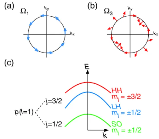
In low-dimensional systems, the Rashba SOI becomes more important because it is stronger at the heterointerface and can be controlled by an external electric field. Many of the pioneering studies on the SOI-induced phenomena mentioned above were performed in two-dimensional elec- tron systems, where the Rashba SOI is described by the k-linear Rashba term. In the Hamiltonian, the k-linear Rashba term can be written asHR1¼α1Eziðk−σþ−kþσ−Þ, where σ¼1=2ðσxiσyÞ denote combinations of Pauli spin matrices,k ¼kxiky, andkx,kyare the components of the in-plane wave vectork∥. The effective magnetic field Ω1ðk∥Þacting on the transport carrier due to the k-linear Rashba term is illustrated in Fig.1(a).
Recently, a higher-order contribution of the Rashba SOI, the so-called k3 (k-cubic) Rashba SOI, has received more attention[14,15]. The Hamiltonian for thek-cubic Rashba SOI is expressed as HR3¼α3Eziðk3−σþ−k3þσ−Þ [16],
and the effective magnetic field Ω3ðk∥Þ in k space is illustrated in Fig.1(b) [15]. There is a significant difference in the effective field symmetry between thek-linear and the k-cubic Rashba SOI with one and three rotations inkspace, respectively. Thek3symmetry of the SOI is an interesting subject because it influences all of the SOI-induced phe- nomena as opposed to the k-linear Rashba term. For example, in case of the spin Hall effect, the k-cubic Rashba term is predicted to give rise to a larger spin Hall conductivity[17–19].
kx ky
kx
ky Ω3
Ω1
(a) (b)
(c)
p(l=1) j=3/2 j=1/2
mj= ±1/2 mj= ±3/2 HH E
k LH SOmj= ±1/2
FIG. 1 (color online). (a),(b) The effective magnetic field direction with respect to the in-plane wave vectorkfor (a) the linear-Rashba term, Ω1 and (b) the cubic-Rashba term, Ω3. (c) Schematic illustration of the valence band structure for strained Ge. The HH, LH, and SO bands are indicated.
Recently, the cubic-Rashba SOI has been reported in a two-dimensional hole gas (2DHG) in inversion asymmetric semiconductors InGaAs and GaAs [20,21], and a two- dimensional electron gas formed at a surface of the inversion symmetric oxide SrTiO3[15]. However in the former case, the InGaAs and GaAs possess both BIA and SIA; thus, they are always influenced by both Dresselhaus and Rashba SOI contributions [22]. Because the Dresselhaus SOI also has k-cubic dependence, the cubic-Rashba SOI is difficult to observe independently. In the latter case, the complex electric structure of SrTiO3 makes it difficult to compare with the existing Rashba theory and theoretical development on the spin orbit interaction in the perovskite oxide is still in progress. Consequently, material systems with a simple band structure and pure cubic-Rashba SOI are in high demand. Here, we propose a purely cubic-Rashba SOI system: the single element semiconductor Ge. Because Ge does not have BIA, the Dresselhaus SOI is essentially absent. Thus, the SOI in Ge is described only with the Rashba term.
The valence band structure of strained Ge around theΓ point is schematically illustrated in Fig. 1(c). The valence band hole has ap-orbital wave function with orbital angular momentuml¼1; therefore, it has total angular momentum j¼3=2andj¼1=2. Thej¼3=2andj¼1=2hole states are separated from each other due to the atomic SOI. The separated j¼1=2state is called the split-off (SO) state as indicated in Fig. 1(c). The j¼3=2state further splits into themj¼ 3=2heavy hole (HH) andmj¼ 1=2light hole (LH) states. Among the hole states, the wave function described by mj¼ 1=2 possesses a k-linear Rashba SOI. The k-linear Rashba SOI is also dominant in most studied conduction band electron cases since the conduction band is fully described by the mj¼ 1=2wave function.
On the other hand, formj¼ 3=2, the Rashba SOI exhibits k-cubic dependence. Further, in the strained-Ge=SiGe quan- tum well (QW) structure, owing to compressive strain in the Ge well, the degeneracy of the HH and LH bands atk¼0 can be lifted. The separation between the HH and LH bands can be as large as ∼100 meV with increasing amounts of strain. Thus, the top of the valence band can be tuned to the HH state. Recent advances in Ge and SiGe epitaxial growth technology revealed that it is possible to fabricate a high crystal quality strained-Ge=SiGe QW on Si substrates [23,24]. Thus, strained Ge=SiGe provides a good platform to study the cubic-Rashba SOI in simple single element semiconductors and will offer an interesting comparison with existing SOI theory.
In this Letter, we experimentally reveal cubic-Rashba SOI in a 2DHG in a strained-Ge=SiGe QW. Comparing the weak localization (WL) and weak antilocalization (WAL) measurements with the analysis of the linear- and cubic- Rashba SOI terms, we found that spin transport in the 2DHG can be fully explained by the cubic-Rashba SOI.
The SOI magnitude can be controlled with the gate voltage.
These findings are all consistent with the mj¼ 3=2 characteristics of the HH band in a strained-Ge QW, which obeys the cubic-Rashba Hamiltonian.
A strained-Ge=SiGe single QW is grown by using solid source molecular beam epitaxy. First, a fully relaxed Si0.5Ge0.5 buffer layer is grown on a Si(001) substrate.
On top of this layer, the following QW structure is grown:
10 p-Si0.5Ge0.5=10 Si0.5Ge0.5=20 Ge=30 Si0.5Ge0.5=3 Si (units in nanometers). Due to the lattice mismatch (∼2.1%) between the Ge and Si0.5Ge0.5 layers, the Ge QW layer is compressively strained. After patterning the wafer in the Hall bar structure, an Al2O3dielectric layer with a 75-nm thickness is deposited using atomic layer deposition, and then a Pd=Au gate electrode is deposited. The application of the gate voltage enables us to tune the hole density of the 2DHG in the QW. The magnetotransport is measured in a variable temperature cryostat at the temperature range of 1.6–10 K. A magnetic field is applied perpendicular to the sample plane using a superconducting magnet.
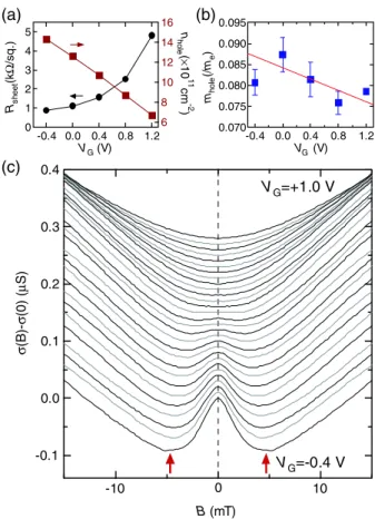
First, the change in the sheet resistance Rsheet and hole concentration nhole at various back gate voltages VG is shown in Fig. 2(a). When VG is decreased from þ1.2 to
−0.4V,Rsheet (nhole) monotonically decreases (increases).
This change accompanies the variation of hole mobility
(a) (b)
(c) 0.4
0.3
0.2
0.1
0.0
-0.1
σ(B)-σ(0)(µS)
-10 0 10
B(mT)
VG=-0.4 V VG=+1.0 V
5 4 3 2 1 0 Rsheet(kΩ/sq.)
1.2 0.8 0.4 0.0 -0.4
VG(V)
16 14 12 10 8 6
nhole(×10 11cm -2)
0.095 0.090 0.085 0.080 0.075 0.070 mhole(/me)
1.2 0.8 0.4 0.0 -0.4
VG(V)
FIG. 2 (color online). (a),(b) TheVG dependence of (a) sheet resistance Rsheet and hole concentration nhole and (b) the hole effective mass mhole. (c) The change of magnetoconductivity ΔσðBÞ measured at 1.6 K at variousVG.
from 2000 to 5200cm2=V s. The change in the hole effective mass mhole with respect to VG is shown in Fig. 2(b). The effective mass of the holes is determined from the temperature dependence of the Shubnikov–de Haas oscillation. The effective mass increases with the hole concentration and this is due to the nonparabolicity of the valence band [25,26].
Next, we show the change of magnetoconductivity ΔσðBÞ ¼σðBÞ−σð0Þ measured at various VG in Fig. 2(c). Under a gate sweep of VG ¼ þ1.0 to −0.4V, ΔσðBÞis significantly modulated. In the high-field region, the conductivity monotonically increases with the external magnetic field, which we attribute to the WL. Together with the WL feature, in the high hole density region (VG<þ0.2 V) a conductance peak appears when the magnetic field is near zero. This conductance peak is due to the WAL. The cross-over points of ΔσðBÞ, which are indicated by arrows in Fig. 2(c), shift position from low magnetic field to high magnetic field with decreasingVG. The cross-over points are roughly proportional to the magnetic field for the SOI,BSO; a larger BSO produces a larger cross-over point field. Thus, our results suggest that the SOI can be tuned with the gate voltage.
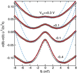
Observed WL and WAL data have been analyzed by using the Iordanskii–Lyanda-Geller–Pikus (ILP) theory for magnetoconductivity, which took into account both the linear- and cubic-Rashba SOI[15,20,27]. The general formula of the ILP theory is provided in the Supplemental Material[28]. We limited our fitting to within the diffusive transport regime where the magnetic fieldB is within the rangeB < Btr¼ℏ=2el2m, whereBtr denotes the transport field characterizing the elastic scattering time of the hole,ℏ is Planck’s constant,eis the electron charge, andlm is the mean free path of the hole. In the ILP theory, we only consider the Rashba SOI since there is no structural inversion asymmetry in Ge. Bothk-linearΩ1andk-cubicΩ3effective magnetic fields in frequency units are incorporated [15].
Under these conditions, the fitting parameters to analyze experimental data are the characteristic magnetic fields for the phase coherence Bϕ¼ℏ=4eDτϕ, for the k-linear spin-orbit couplingBSO1¼ ðℏ=4eDÞ2jΩ1j2τtr, and for the k-cubic spin-orbit coupling BSO3¼ ðℏ=4eDÞ2jΩ3j2τtr, where D denotes the diffusion constant, τϕ the phase coherent time of the carrier, and τtr the elastic scattering time. By setting either BSO3¼0 or BSO1¼0 in the ILP model, formulas with only thek-linear term or thek-cubic term are obtained[28]. In Fig.3, we present the experimental data (open circles) and fitting results with only thek-linear term (blue dashed line) or only thek-cubic term (red solid line). We found that fitting with only the cubic-Rashba term revealed good agreement with the experimental results regardless of theVGvalue, whereas the linear-Rashba term is insufficient for explaining the larger field region of the WAL data. The low magnetic field region can be fitted with both the linear- and cubic- models because this region is
determined by theBϕ term rather than BSO. However, we observed significantly different behavior between the linear- and cubic-Rashba terms in the larger magnetic field region.
The cubic-Rashba model explains the experimental data more precisely; thus, we believe the cubic-Rashba model is relevant for the HH band in Ge.
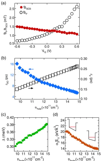
Figure4(a)showsBSO3andBϕobtained by fitting with the cubic-Rashba model. BothBSO3andBϕsystematically change withVG. WhenBSO3 > Bϕ, WAL is observed, and WL is observed when BSO3 < Bϕ. The change of BSO3 provides direct evidence of the electric field control of the cubic-Rashba SOI. Note that the change ofBϕwith respect to VG is due to the change of the hole mobility, and this gives rise to a longer phase coherence time τϕ with increasing hole concentration. If k-dependent spin splitting due to the SOI exists, the spin relaxation is described by the Dyakonov-Perel mechanism with τSO∝ 1=Δ2τtr[29], whereΔis the spin splitting energy and τSO
denotes the spin relaxation time. On the other hand, if spin- flip scattering is the dominant spin relaxation mechanism, the Elliot-Yafet mechanism with τSO∝τtr=ðΔgÞ2 (Δg is the shift of the electrongfactor from that of free electrons) is relevant for describing our results. Therefore, the comparison between τSO and τtr provides additional evi- dence for the Rashba-type SOI. TheτSO andτtrterms can be calculated using the relations BSO3¼ℏ=4eDτSO, D¼v2Fτtr=2,vF ¼ℏkF=mhole, andkF¼ ffiffiffiffiffiffiffiffiffiffiffiffiffiffi
2πnhole
p , where
vF is the Fermi velocity andkF is the Fermi wave vector.
We plotted τSO and τtr with respect to the hole concen- tration as shown in Fig.4(b). We found thatτtr increases with increasing carrier concentration, whereas τSO
decreases. This is consistent with the Dyakonov-Perel spin relaxation mechanism. Therefore, it provides further
-0.10 -0.05 0.00 0.05 0.10
σ(B)-σ(0)(2 /2π2 )
-8 -6 -4 -2 0 2 4 6 8
B(mT) VG=+0.3 V
+0.1
-0.1
-0.4
FIG. 3 (color online). The VG dependence of the change of magnetoconductivityΔσðBÞ shown with the fitting results from the ILP model. Black open circles indicate experimental data, and the red solid line and blue dashed lines show calculations using the ILP model for the cubic- and linear-Rashba terms, respectively.
evidence that the Rashba SOI is a dominant spin-orbit contribution in the 2DHG.
The agreement between the experimental data and the k-cubic-term-only condition of the ILP theory reveals the existence of the purely cubic-Rashba SOI in the 2DHG.
We now evaluate the spin splitting energy from the relationship Δ¼ℏjΩ3j. The change ofΔ with respect to hole concentration is shown in Fig.4(c). We obtained aΔ of 0.3–0.4 meV; we find larger spin splitting with increas- ing hole concentration. This spin splitting provides direct experimental evidence of the cubic-Rashba SOI induced splitting in strained Ge. To analyze the splitting in more detail, we calculated the coefficient α3Ez for the cubic- Rashba SOI using the relation Δ¼ℏjΩ3j ¼α3Ezk3, as shown in Fig. 4(d). The coefficient α3Ez decreases with increasing hole concentration. We believe that this is due to
the change of the gate-induced electric fieldEzin the QW rather than a change ofα3.
Here, the Rashba coefficientα3for the first HH subband is expressed as follows:
α3¼ −3eℏ4γ23 2m20
EHH−ELH2; ð1Þ
whereγ3denotes the Luttinger parameter, andEHHandELH are the energies of the lowest HH and LH subbands, respectively. Equation (1) is derived from the Luttinger Hamiltonian using the partitioning method presented by Ohkawa and Uemura[13]. Equation(1)suggests thatα3is inversely proportional to the square of the separation between the HH and LH energy. A qualitatively similar expression to Eq. (1) is also reported by other groups [14,20]. In a single heterostructure, the HH-LH separation changes with the external electric field, thus demonstrating gate control ofα3[30]. However, in the QW, the change in the HH and LH separation with external electric field should be small. Furthermore, because the HH-LH separation in the Ge=Si0.5Ge0.5 QW is initially large due to strain, the gate- induced change of the HH-LH separation is 1 order smaller than its total HH-LH separation energy; therefore, we think thatα3is almost constant over the studied hole concentration range. For these reasons, we believe that the results shown in Fig.4(d)reflect the change of the effective electric field in the QW under the application of the gate voltage. Because the gate-induced electric field in the QW opposes the initial electric field due to modulation doping on the bottom side of the QW, the increase of the hole concentration in the QW decreases its internal electric field. Thus, α3Ez decreases with increasing hole concentration.
Equation (1)suggests another interesting aspect of the cubic-Rashba coefficient. The Rashba coefficient can be strongly tuned with the HH-LH separation. We estimated α3 using Eq.(1) with γ3¼5.69for Ge [1]. The HH-LH separation for compressively strained-Ge=Si0.5Ge0.5 is
∼110meV [31]. We obtained α3¼2.26×10⁵eÅ4. The coefficient α3 is about 1 order smaller than for the 2DHG in the GaAs/AlGaAs single heterostructure [21], which is a nearly lattice matched system. The smallerα3 value is due to the large HH-LH separation in Ge=Si0.5Ge0.5 compared to that of the GaAs/AlGaAs structure; the large HH-LH separation decreases the coefficient α3. In the strained-Ge=SiGe QW, the HH-LH separation can be tuned by the strain due to the SiGe layer; in other words, the compositionxof the Si1−xGex buffer layer enables a wide range of tuning options for the cubic-Rashba SOI. Note that Ge has a largerγ3value than Si (γ3¼1.45)[1]; thus we expect a larger SOI for the 2DHG in Ge than that of Si. Therefore strained Ge is a promising material for utilizing the cubic- Rashba SOI in a low dimensional system.
(a)
(b)
(c) (d)
G
2.5 2.0 1.5 1.0 0.5 Bφ,BSO3(mT)
-0.6 -0.3 0.0 0.3 0.6
V (V) BSO3
Bφ
0.30 0.25 0.20 0.15 0.10 τtr(ps)
15 14 13 12 11 10
nhole(×1011cm-2) 16
12
8
4 τSO(ps)∆(
0.42 0.39 0.36 0.33 0.30
meV)
15 14 13 12 11 10
nhole(×1011cm-2)
24 22 20 18 16 14 α3Ez(eVÅ3 )
15 14 13 12 11 10
nhole(×1011cm-2)
FIG. 4 (color online). (a) TheVGdependence of the character- istic magnetic fields for thek-cubic spin-orbit couplingBSO3and the phase coherenceBϕ. (b) Hole concentration dependence of the spin relaxation timeτSOand momentum scattering timeτtr. (c) Spin-splitting energyΔversus the hole concentration. (d) The change of Rashba spin-orbit coefficientα3Ez with respect to the hole concentration.
We appreciate valuable discussions with H. Nakamura.
This work was partly supported by Grants-in-Aid for Scientific Research (Grants No. 24684024, No. 24340065, No. 25600079, and No. 26286044) from the Japan Society for the Promotion of Science (JSPS), the Project for Developing Innovation Systems of the Ministry of Education, Culture, Sports and Technology, the Deutsche Forschungsgemeinschaft via SFB 631 and the Nanosystems Initiative Munich, and the Hitachi Metals·Materials Science Foundation.
*moriyar@iis.u‑tokyo.ac.jp
†tmachida@iis.u‑tokyo.ac.jp
‡Present address: Graduate School of Engineering, Nagoya University, Nagoya 464-8603, Japan.
[1] R. Winkler,Spin-Orbit Coupling Effects in Two-Dimensional Electron and Hole Systems (Springer Berlin Heidelberg, 2003).
[2] T. Koga, J. Nitta, and M. van Veenhuizen,Phys. Rev. B70, 161302 (2004).
[3] T. Koga, Y. Sekine, and J. Nitta,Phys. Rev. B74, 041302 (2006).
[4] B. A. Bernevig, J. Orenstein, and S.-C. Zhang,Phys. Rev.
Lett.97, 236601 (2006).
[5] J. D. Koralek, C. P. Weber, J. Orenstein, B. A. Bernevig, S.-C. Zhang, S. Mack, and D. D. Awschalom, Nature (London)458, 610 (2009).
[6] J. E. Hirsch,Phys. Rev. Lett.83, 1834 (1999).
[7] S. Murakami, N. Nagaosa, and S.-C. Zhang,Science301, 1348 (2003).
[8] Y. K. Kato, R. C. Myers, A. C. Gossard, and D. D. Awschalom, Science306, 1910 (2004).
[9] C. L. Kane and E. J. Mele, Phys. Rev. Lett. 95, 146802 (2005).
[10] B. A. Bernevig and S.-C. Zhang, Phys. Rev. Lett. 96, 106802 (2006).
[11] G. Dresselhaus,Phys. Rev. 100, 580 (1955).
[12] E. I. Rashba, Sov. Phys. Solid State2, 1109 (1960).
[13] F. J. Ohkawa and Y. Uemura, J. Phys. Soc. Jpn.37, 1325 (1974).
[14] R. Winkler, D. Culcer, S. J. Papadakis, B. Habib, and M. Shayegan, Semicond. Sci. Technol. 23, 114017 (2008).
[15] H. Nakamura, T. Koga, and T. Kimura,Phys. Rev. Lett.108, 206601 (2012).
[16] L. G. Gerchikov and A. V. Subashiev, Sov. Phys. Semicond.
26, 73 (1992).
[17] J. Schliemann and D. Loss, Phys. Rev. B 71, 085308 (2005).
[18] O. Bleibaum and S. Wachsmuth,Phys. Rev. B74, 195330 (2006).
[19] T. Ma and Q. Liu,Phys. Rev. B 73, 245315 (2006).
[20] G. M. Minkov, A. A. Sherstobitov, A. V. Germanenko, O. E.
Rut, V. A. Larionova, and B. N. Zvonkov,Phys. Rev. B71, 165312 (2005).
[21] R. Winkler, H. Noh, E. Tutuc, and M. Shayegan,Phys. Rev.
B 65, 155303 (2002).
[22] J. P. Lu, J. B. Yau, S. P. Shukla, M. Shayegan, L. Wissinger, U. Rössler, and R. Winkler, Phys. Rev. Lett. 81, 1282 (1998).
[23] A. Dobbie, M. Myronov, R. J. H. Morris, A. H. A. Hassan, M. J. Prest, V. A. Shah, E. H. C. Parker, T. E. Whall, and D. R. Leadley,Appl. Phys. Lett.101, 172108 (2012).
[24] K. Sawano, K. Toyama, R. Masutomi, T. Okamoto, N.
Usami, K. Arimoto, K. Nakagawa, and Y. Shiraki, Appl.
Phys. Lett.95, 122109 (2009).
[25] T. Irisawa, M. Myronov, O. A. Mironov, E. H. C. Parker, K.
Nakagawa, M. Murata, S. Koh, and Y. Shiraki,Appl. Phys.
Lett.82, 1425 (2003).
[26] B. Rößner, G. Isella, and H. v. Känel,Appl. Phys. Lett.82, 754 (2003).
[27] S. V. Iordanskii, Y. B. Lyanda-Geller, and G. E. Pikus, JETP Lett.60, 206 (1994).
[28] See Supplemental Material at http://link.aps.org/
supplemental/10.1103/PhysRevLett.113.086601for details of the ILP theory used for fitting.
[29] I.Žutić, J. Fabian, and S. Das Sarma,Rev. Mod. Phys.76, 323 (2004).
[30] B. Habib, E. Tutuc, S. Melinte, M. Shayegan, D. Wasserman, S. A. Lyon, and R. Winkler, Appl. Phys. Lett. 85, 3151 (2004).
[31] M. V. Fischetti and S. E. Laux, J. Appl. Phys. 80, 2234 (1996).