Realizing spin qubits in 28 Si/SiGe:
heterostructure gating, qubit decoherence and asymmetric charge sensing
DISSERTATION ZUR ERLANGUNG DES DOKTORGRADES DER NATURWISSENSCHAFTEN (DR. RER. NAT.) DER
FAKULTÄT FÜR PHYSIK
DER UNIVERSITÄT REGENSBURG
vorgelegt von
Die Arbeit wurde angeleitet von Prof. Dr. Dominique Bougeard.
Contents
1. Introduction 1
2. Fundamental concepts 5
2.1. Silicon and germanium material system . . . . 5
2.2. Si/SiGe heterostructures . . . . 7
2.3. Magnetotransport properties of two dimensional electron gases . . . 9
2.4. Quantum dots in Si/SiGe . . . . 10
2.4.1. Coulomb blockade . . . . 12
2.4.2. Coulomb diamonds . . . . 13
2.5. Double quantum dots . . . . 15
2.6. Single electron in magnetic field . . . . 17
2.7. Electric dipole spin resonance using a magnetic field gradient . . . . 18
3. Gating of undoped Si/SiGe 2DEG 21 3.1. Growth and semiconductor layer structure . . . . 21
3.1.1. Molecular beam epitaxy . . . . 21
3.1.2. Post-growth processing . . . . 23
3.2. Hall measurement . . . . 24
3.2.1. Hall bar sample layout . . . . 24
3.2.2. Accumulation of charge carriers in undoped Si/SiGe . . . . . 26
3.2.3. Magnetotransport characterization . . . . 26
3.3. Introduction to the gating regimes of undoped Si/SiGe . . . . 28
3.4. Biased cool-down . . . . 33
4. Tuning of a single quantum dot to the last electron regime 47
4.1. Device layout and fabrication . . . . 47
4.1.1. Improvements to the gate design . . . . 47
4.1.2. Robust fabrication of the depletion gate layer . . . . 49
4.2. Charge sensor optimization . . . . 50
4.2.1. Initial sensor characterization . . . . 50
4.2.2. A different charge sensor configuration . . . . 52
4.3. Depletion to the last electron . . . . 52
4.3.1. Initial qubit dot region characterization . . . . 52
4.3.2. Suppressing unintentional quantum dots and the last electron 53 4.4. Conclusion . . . . 54
5. Relaxation study on single electron spins 57 5.1. Energy selective spin readout . . . . 57
5.1.1. Spin-to-charge conversion . . . . 57
5.1.2. Spin-up and -down signal . . . . 58
5.1.3. Measurement of the tunnel barriers . . . . 60
5.2. T 1 relaxation study . . . . 62
5.2.1. Load time variation yields T 1 time . . . . 62
5.2.2. T 1 ( B ) spectroscopy and valley hotspot . . . . 63
5.3. Valley splitting across multiple gate voltage configurations . . . . 66
5.3.1. Self-consistent Schrödinger-Poisson simulations . . . . 67
5.3.2. Orbital splitting . . . . 68
5.3.3. Valley splitting in proximity to a monolayer step . . . . 70
5.4. Conclusion . . . . 71
6. Single spin manipulation in 28 Si/SiGe 73 6.1. Spin manipulation by electric dipole spin resonance . . . . 73
6.1.1. Rabi oscillation measurement . . . . 74
6.2. Dephasing time T 2 ∗ . . . . 76
6.2.1. Accessing dephasing with the Ramsey pulse scheme . . . . . 76
6.2.2. Ramsey fringe measurement . . . . 76
6.2.3. Extracting T 2 ∗ dependent on measurement time . . . . 78
6.3. Refocusing slow noise by Hahn echo . . . . 79
6.4. Conclusion . . . . 81
Contents
7. Asymmetric sensing dot 83
7.1. Concept of a new kind of charge sensor . . . . 83
7.1.1. Enhancement of signal-to-noise with a transistor . . . . 83
7.1.2. Conventional quantum dot charge sensor . . . . 84
7.1.3. Increasing the voltage swing . . . . 86
7.2. Device layout and engineering of the electrostatic potential . . . . . 86
7.2.1. Decreasing capacitive coupling . . . . 86
7.2.2. Fabrication optimization . . . . 88
7.2.3. Feedback to the simulation . . . . 90
7.3. Instabilities in asymmetric sensing dot (ASD) devices . . . . 92
7.4. Asymmetric Coulomb diamonds . . . . 93
7.4.1. Proof of concept by slide gate variation . . . . 94
7.4.2. Slide potential variation . . . . 98
7.5. Conclusion and outlook . . . . 99
8. Conclusion and Outlook 101 A. Appendix 105 A.1. Determination of source lever arm of conventional charge sensor . . . 105
A.2. Measurement setup information . . . 106
A.2.1. He dewar with magnet insert . . . 106
A.2.2. Dilution refrigerator setup . . . 106
A.2.3. 3 He-cryostat . . . 106
A.3. Simulation details . . . 107
A.4. Details on the fabrication . . . 107
A.4.1. Hall bar samples . . . 107
A.4.2. DQD and ASD devices . . . 108
A.4.3. Optical lithography recipe . . . 109
A.4.4. Gate lines with LOR3A resist . . . 110
Acronyms 127
Acknowledgments 129
1. Introduction
Since the advent of computing, this technology has brought substantial economic growth and scientific discoveries. This success is based on the ability for computers to solve some kinds of problems faster than humans. However, there is still a class of intractable problems that is hard to solve for classical computers, meaning that the computing time and memory scale exponentially with the problem size [1]. A new kind of computer, harnessing the quantum superposition and entanglement for computation, should be able to solve some of these problems in polynomial time [1, 2]. Such a universal quantum computer is proven to solve problems such as prime factorization, finding discrete logarithms, solving linear systems of equations and searching unsorted data faster than its classical counterpart for large problem sizes [3–
6]. Apart from these applications, a quantum computer is predicted to be highly efficient in simulating physical systems governed by quantum mechanics, offering insights which would be hard to obtain in the real system [7–10]. For example, the development of drugs could be sped up by quantum simulation [11].
The fundamental building block of a quantum computer is the qubit: a two-level quantum system allowing the superposition of the levels as well as the entanglement between multiple qubits. Qubits can be realized in a multitude of physical systems including photons, trapped ions and superconducting circuits [12–15].
The field of quantum computing is currently in a stage of noisy intermediate-scale
quantum technology, where around 50 noisy qubits have been demonstrated in a
single device [16, 17]. Although quantum supremacy, the point where it takes longer
to calculate a specific algorithm in a classical supercomputer than on a quantum
turing techniques and the good tunability of the confinement potential [20]. Most of the preliminary work in this branch of quantum computing research was done in GaAs, building on advancements in quantum-transport-, Coulomb-blockade- and spin-blockade-physics [21]. Yet, the strong fluctuating Overhauser field of the host nuclei and the strong spin-orbit coupling strength were limiting the qubit coherence with dephasing times in the order of 10 ns [22–24].
By moving to silicon as the basis for gate-defined quantum dots, with only 4.685 % of the nuclear spin carrying isotope 29 Si in the natural Si composition and a weak spin-orbit interaction, the interaction of the spin with its environment is reduced [25–
32]. The isotopical purification of 28 Si allows to engineer a virtually nuclear-spin-free host material [33–35]. These improvements yielded remarkable dephasing times in the order of 120 µs in metal oxide semiconductor (MOS) structures [31] and 20 µs for electron spin qubits in 28 Si/SiGe heterostructures [36, 37] with control-fidelities surpassing 99.9 % [36].
In our group, we have developed a qubit platform based on gate-defined quantum dots (QDs) in 28 Si/SiGe heterostructures in previous work [38–40]. The heterostruc- tures intended for qubit experiments feature a quantum well (QW) which is grown by means of molecular beam epitaxy (MBE) using an isotopically purified 28 Si source crystal with only 60 ppm of remaining 29 Si. Combining this MBE-grown heterostruc- ture with a magnet placed in the plane of the QD-defining gate layer, we have a unique framework for qubit realization in a collaborative effort with the group of Lars Schreiber at the RWTH Aachen. Previous work demonstrated single electron operation in our qubit platform.
In this thesis we set out to deepen our understanding of the heterostructure properties to reach high-yield single electron tuning, since for example charge recon- figurations in defect trap states impede the device tuning. In parallel, a demonstration of qubit operation and with this a measurement of qubit characteristics such as relaxation and dephasing times remained as the aim of this thesis.
The current research in quantum computing is moving towards qubit operation at temperatures around 1 K where more cooling power is available in the refrigerators, in an effort towards the integration of control electronics in vicinity of the qubits [41].
Signal-to-noise ratio (SNR) and bandwidth plays an important role for a robust and
fast measurement of the spin, especially at elevated temperatures [42]. A new kind
of charge sensor, presented in the last part of this thesis, is a promising candidate to
deliver these features.
This thesis is organized as follows:
• In chapter 2 we will discuss the fundamental theoretical concepts required for a basic understanding of the experimental studies presented in this thesis.
• In chapter 3 we will present a characterization of the gated undoped Si/SiGe heterostructures building the basis for our nanostructure devices.
• In chapter 4 we will show the initial tuning of a single quantum dot with an adjacent charge sensor in 28 Si/SiGe.
• In chapter 5 we will demonstrate the spin-to-charge conversion and study the spin relaxation in order to extract the valley splitting in our qubit device.
• In chapter 6 we will introduce the spin manipulation via electric dipole spin resonance (EDSR) and access the dephasing and decoherence times in our qubit.
• In chapter 7 we will study a concept for a new kind of charge sensor aiming
towards a large SNR and high bandwidth spin readout.
2. Fundamental concepts
In this chapter, we will discuss the underlying concepts required for an understanding of the experiments studied in this thesis.
2.1. Silicon and germanium material system
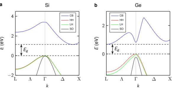
The devices studied in this thesis are based on Si/SiGe QW-heterostructures. There- fore, we first turn towards the properties of this material system. Fig. 2.1 shows the simulated band structure of silicon (a) and germanium (b). Both materials are indirect semiconductors, which manifests in a conduction band minimum that is not at the Γ-point of the Brillouin . The band gaps of Si and Ge have been determined to 1.12 eV and 0.661 eV, respectively [43, 44]. Both elements crystallize in a diamond lattice with lattice constants of a Si = 543.1 pm for silicon and a Ge = 565.8 pm for germanium [43, 44]. The two elements are miscible into the alloy Si 1−x Ge x with any desired Ge content x. The resulting lattice constant a 0 (x) of the Si 1−x Ge x is described by Vegard’s law [45]
a 0 ( x ) = a Si (1 − x ) + a Ge x . (2.1)
Fig. 2.2 a shows the band gap for relaxed Si 1 –x Ge x bulk material with a monotonous
decrease in band gap for increasing Ge content x . Despite of the larger band gap
of pure Si compared to any Si 1 – x Ge x alloy, it is possible to engineer a Si-QW
heterostructure.
E g
L Γ X
−2 0 2 4
Λ ∆
k
E (eV)
Si
CB HH LH SO
a
E g
L Γ X
0 2
Λ ∆
k
E (eV)
Ge
CB HH LH SO
b
Figure 2.1. – a The band structure of silicon with the conduction (blue), heavy-hole (red), light-hole (green) and split-off (black) bands. The indirect band gap of Si with E g = 1.12 eV. b The band structure of germanium with an indirect band gap of E g = 0.661 eV. Simulated with [46]. Adapted from [47].
a
[010]
[001]
[100]
x
x x
x x
x Γ
b
Figure 2.2. – a The band gap of unstrained Si 1 – x Ge x as a function of the Ge content x is shown in the upper line. The nature of the band gap is Si-like with the conduction band minimum lying in the ∆-direction for x < 0.85 and Ge-like with the conduction band minimum located at the L point of the Brillouin zone for x > 0.85. The lower lines cover strained Si 1 – x Ge x which is not covered in this thesis. Republished with permission of IOP Publishing, Ltd and AIP Publishing, from [48, 49]; permission conveyed through Copyright Clearance Center, Inc.
b The surfaces of constant energy close to the conduction band minima in the Si Brillouin zone forming ellipsoids. In the case of biaxial tensile strain applied to bulk Si in the [100] and [010] directions, the ellipsoids in the [001] direction (shown in blue) are shifted lower in energy, while the ellipsoids in the [100] and
[010] directions are shifted up in energy.
2.2. Si/SiGe heterostructures
2.2. Si/SiGe heterostructures
When Si is grown onto a relaxed Si 1 – x Ge x substrate, the Si lattice adapts to the larger SiGe lattice constant, introducing strain in the Si layer. This strain lifts the sixfold valley degeneracy present in bulk Si, as depicted in Fig. 2.2 b. The twofold degenerate ∆ 2 valleys are shifted down in energy and the fourfold degenerate ∆ 4
valleys are shifted up in energy in the strained Si. Furthermore, the twofold ground state degeneracy is lifted by the QW confinement potential leading to the valley splitting E V S [50]. The band gap of the strained Si gets reduced, which leads to a type-II band alignment in a Si/Si 1 – x Ge x QW heterostructure [39].
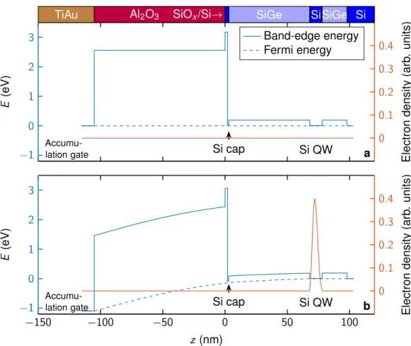
Fig. 2.3 a shows the simulated conduction band edge energy as a function of the coordinate in growth direction z in an undoped Si/SiGe QW heterostructure. Due to the absence of doping, the band edge energy is flat with steps due to differences in the material composition. The Si QW as well as the Si cap represent a minima of the conduction band edge energy. In this flat-band condition the first subband in the QW is above the Fermi energy indicated by the dashed line and no electrons are allowed to enter the QW, indicated by the zero electron density in Fig. 2.3 a.
Therefore, it is mandatory to add a gate oxide and a metal layer further referred to as accumulation gate, located at z < 0 nm, in order to manipulate the band edge energy. A positive voltage applied to the TiAu accumulation gate lowers the band edge energy, as shown in Fig. 2.3 b, eventually leading to the first subband energy in the QW shifting below the Fermi energy. This allows electrons to enter the QW, indicated by the non-zero electron density in the QW region. When only the first subband is occupied, the electrons form a two dimensional electron gas (2DEG).
Note that no electron density is predicted to accumulate in the 1 nm Si cap, as the
larger confinement energy contribution keeps the first subband energy above the
Fermi energy. The 2DEG can be characterized by magnetotransport studies, which
will be covered in the following section.
−1 0 1 2 3
E (eV)
Band-edge energy Fermi energy
0 0.1 0.2 0.3 0.4
Si QW Si cap
Accumu-
lation gate a
TiAu Al 2 O 3 SiO x /Si→ SiGe SiSiGe Si
Electron density (arb . units)
−150 −100 −50 0 50 100
−1 0 1 2 3
z (nm)
E (eV)
0 0.1 0.2 0.3 0.4
Si QW Si cap
Accumu-
lation gate b
Electron density (arb . units)
Figure 2.3. – The simulated conduction band edge energy of a Si/SiGe het-
erostructure with an Al 2 O 3 gate oxide and a metal accumulation gate as a
function of the coordinate z oriented along the growth direction (blue). The
simulated electron density as a function of z is plotted in orange. a The flat band
structure in the case of 0 V applied to the accumulation gate with respect to the
grounded QW. As the first subband in the QW is above the Fermi energy, no
charge carriers are allowed in the QW resulting in zero electron density. b Here,
1.1 V is applied to the accumulation gate, resulting in a band bending which
induces a non-zero charge carrier density in the QW as the first subband moves
below the Fermi energy. Adapted from [47].
2.3. Magnetotransport properties of two dimensional electron gases
2.3. Magnetotransport properties of two dimensional electron gases
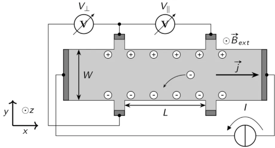
A 2DEG patterned in a Hall bar geometry is schematically depicted in Fig. 2.4, with the ohmic contacts indicated by the dark gray regions. A typical magnetotransport measurement accesses the longitudinal and transversal resistivities ρ xx and ρ xy in a four-point measurement of the longitudinal and transversal resistance V k /I and V ⊥ /I , respectively and the consideration of the Hall bar width and length dimensions:
ρ xx = V k I
W
L (2.2)
ρ xy = V ⊥
I . (2.3)
The out-of-plane magnetic field B ext is varied and due to the Lorentz-force acting upon the moving charge carriers, a non-zero Hall resistance is detected. In the regime described by the classical Hall effect [51], V ⊥ rises linearly with the magnetic field while V k stays constant. The resulting longitudinal and transversal resistivities are described by
ρ xx = m ∗ ne 2 τ = 1
neµ and (2.4)
ρ xy = B ext
en , (2.5)
where m ∗ is the effective mass of the charge carriers, e is the elementary charge, n is the charge carrier density, τ is the mean scattering time and µ = m eτ
∗is the charge carrier mobility [52].
The Fermi wave vector is then described by
k F =
s 4πn , (2.6)
The mean free path l is a measure for the average length the charge carriers travel between two scattering events.
By confining the 2DEG in the two in-plane dimensions, it is possible to create QDs in the Si host material. We will discuss the characteristic properties of these systems in the following section.
L W
#» j -
+
-
+
-
+
-
+
-
+
-
+
- V
V ⊥
V V k
I #»
B ex t
x
y z
Figure 2.4. – A schematic illustration of a Hall bar sample with width W and segment length L . A current density ~j is injected in the x direction. The external magnetic field B ~ ext is oriented along the z direction, leading to a deflection of the electrons due to the Lorentz force. Charges accumulate on the edges of the sample, inducing a non-zero transversal voltage V ⊥ .
2.4. Quantum dots in Si/SiGe
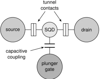
An island formed in the 2DEG due to lateral confinement, commonly referred to as single quantum dot (SQD), coupled to the source and drain reservoirs via tunnel contacts is illustrated in Fig. 2.5. A plunger gate is capacitively coupled to the SQD.
This structure is commonly approximated by a circular disc in the 2DEG with a radius r and an electron charge of −eN for N electrons occupying the SQD. The self-capacitance of this disc is described by
C = 8 0 r , (2.9)
with being the dielectric constant of the surrounding material, which is assumed to
be homogeneous in this approximation, and the vacuum permittivity 0 [52]. The
2.4. Quantum dots in Si/SiGe
electrostatic energy of the island is then given by E elstat ( N ) = e 2 N 2
2 C = e 2 N 2
16 0 r . (2.10)
The energy required to add the ( N + 1)-th onto a SQD occupied with N electrons is the difference between the electrostatic energies
E c ( N + 1) = E elstat ( N + 1) − E elstat ( N ) = e 2 C
N + 1
2 N 1
≈ e 2
C N = e 2 8 0 r N .
(2.11) However, the term charging energy is commonly used for
∆ E c = E c ( N + 1) − E c ( N ) = e 2
C = e 2
8 0 r . (2.12)
For a SQD with a radius of 50 nm and = 11.7 of Si this characteristic energy scale is ∆ E c ≈ 3.9 meV, which corresponds to a temperature of 45 K.
The single-particle level spacing can be approximated using the model of a quantum mechanical harmonic oscillator [52]
∆ = ~ ω 0 = ~ 2
4 m ∗ r 2 . (2.13)
For a SQD in Si with m ∗ = 0.19 m e and a radius of 50 nm, this energy scale computes to 40 µeV or a temperature of 0.5 K. This is two orders of magnitude smaller than ∆ E c indicating that the total energy of the SQD is governed by the Coulomb interaction energy for the laterally defined SQDs studied in this thesis.
Considering the capacitively coupled plunger gate shown in Fig. 2.5, the ground state energy for a SQD occupied with N electrons depends on the plunger gate voltage V pg
E N ( V pg ) = E N ( V 0 ) − eN α pg ( V pg − V 0 ), (2.14)
source SQD drain
plunger gate tunnel contacts
capacitive coupling
Figure 2.5. – A schematic depiction of a SQD with tunnel contacts to source and drain reservoirs. The plunger gate couples capacitively onto the SQD.
2.4.1. Coulomb blockade
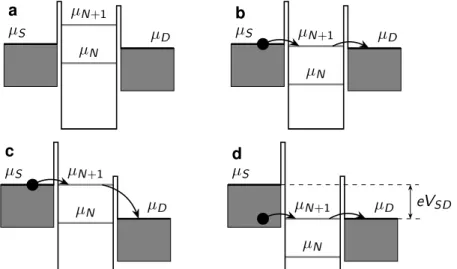
Fig. 2.6 shows a schematic representation of the energetic situation for a SQD in between source and drain reservoirs. The electronic levels in the source and drain reservoirs are filled up to the electrochemical potentials µ S and µ D , respectively, in the case of low temperatures. We first consider the situation where only a small bias voltage is applied between the reservoirs. In Fig. 2.6 a the SQD is occupied with N electrons, as µ N < µ D < µ S . However, the energy required to add the ( N + 1)-th electron onto the SQD is not available, as µ N+1 > µ S > µ D . This leads to a constant occupation of the SQD with the same N electrons, which effectively blocks the current flowing between the source and drain reservoirs. This situation is commonly termed Coulomb blockade since the Coulomb interaction prevents a ( N + 1)-th electron to enter the SQD. Using the plunger gate voltage, combining
Eqs. 2.14 and 2.15 the electrostatic potential can be tuned with
µ N ( V pg ) = µ N ( V pg 0 ) − eα pg ( V pg − V pg 0 ). (2.16)
Fig. 2.6 b shows the situation where Coulomb blockade is lifted, by tuning µ N +1 to a
value in between µ S and µ D by a change of V pg . In this situation either N + 1 or N
electrons can occupy the SQD, allowing for sequential transport of electrons through
the SQD, indicated by the arrows in Fig. 2.6 b.
2.4. Quantum dots in Si/SiGe
2.4.2. Coulomb diamonds
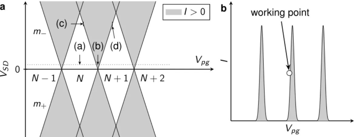
Considering the current through the SQD as a function of the bias voltage V SD and V pg , we expect the regions of suppressed current to form diamond shaped regions, as depicted in Fig. 2.7 a. The grey regions mark a transport current through the SQD.
The borders of the blockade regions, commonly referred to as Coulomb diamonds, mark the configurations of V SD and V pg where either of the reservoir chemical potentials is aligned with a SQD chemical potential, as schematically depicted in Fig. 2.6 c for µ S = µ N+1 and Fig. 2.6 d for µ D = µ N+1 . We mark the configurations in Fig. 2.7 a with the labels corresponding to the subfigures in Fig. 2.6.
µ S µ D
µ N µ N+1 a
µ S µ D
µ N µ N+1 b
µ S
µ D µ N
µ N+1 c
µ S
µ D µ N
µ N+1 eV SD
d
Figure 2.6. – A schematic illustration of the electrochemical potentials in a SQD occupied with N electrons with small (a, b) and large (c, d) source- drain bias voltages. a There are no energy levels in the QD lying in between the electrochemical potentials of source and drain µ S and µ D . The system is considered to be in Coulomb blockade as no electron transport is allowed. b The level µ N+1 lies in the source-drain bias window and sequential tunneling of electrons is allowed. c µ N +1 is aligned with µ S and transport is allowed. d µ N+1
is equal to and current is allowed to flow. The difference in the source and
m − in Fig. 2.7 a, satisfy
∆ µ N = µ D = 0, (2.17)
meaning that the capacitive coupling of the source reservoir and the plunger gate keeps the SQD electrostatic potential aligned with the potential of the grounded drain reservoir. The shift in µ N in response to changes of ∆ V SD and ∆ V pg can be described by
∆ µ N = −e ∆ V SD C S
C and (2.18)
∆ µ N = + e ∆ V pg
C pg
C . (2.19)
Here, C S describes the capacitive coupling of the source reservoir onto the SQD.
Dividing Eq. 2.18 by Eq. 2.19, we get an equation for the negative slope m − of the diamond borders described by Eq. 2.17
m − = ∆ V SD
∆ V pg = − C pg
C S = − α pg
α S (2.20)
with the source lever arm
α S = C S
C . (2.21)
In a similar fashion we can derive the slope of the positively sloped diamond borders m + = C pg
C − C S . (2.22)
Inserting Eqs. 2.20 and 2.22 in Eq. 2.21, we can express the source lever arm as a function of the negative ( m − ) and positive ( m + ) diamond border slopes
α S = m +
m + − m −
m
+>0; m
−<0
= |m + |
|m + | + |m − | . (2.23)
Fig. 2.7 b shows the current I through the SQD as a function of V pg for a small fixed
V SD indicated by the dotted line in Fig. 2.7 a. Peaks in I are expected when the
Coulomb blockade is lifted. On each side of the peaks, d I/ d V pg is large, yielding a
large change in I for a small change in V pg . In the same way the current signal is
sensitive to changes in V pg , it is also sensitive to any other changes to the electrostatic
potential. An electron entering or leaving a nearby QD may induce such a change in
2.5. Double quantum dots
the electrostatic potential, which can be detected in the change of the current flowing through the SQD. Thus we can employ a SQD as a charge sensor for nearby QDs.
This is especially useful in configurations where the tunnel barriers are too opaque for the tunnel current to be detected. The sensor has to be in the regime with large d I/ d V pg in order to have a large sensitivity, indicated by the working point marked in Fig. 2.7 b.
0
N − 1 N N + 1 N + 2 (a) (b)
(c)
(d) m −
m +
V pg V S D
I > 0
a working point
V pg
I
b
Figure 2.7. – a A schematic illustration of the current through a SQD as
a function of the source-drain voltage V SD and the plunger gate voltage V pg .
The regions with significant current flow are indicated in grey, while the white
regions mark the Coulomb diamonds, where current flow is suppressed due to
Coulomb interaction. The points marked with the labels (a) to (d) correspond
to the configurations depicted in Fig. 2.6. The electron occupation of the SQD,
indicated by the labels from (N-1) to (N+2), stays constant inside each Coulomb
diamond. b The schematic current I through a SQD as a function of V pg at the
bias voltage indicated by the dotted line in a . Sharp Coulomb peaks emerge
where the Coulomb blockade is lifted. Choosing a working point on the side of a
peak, as indicated by the circle, the SQD can be used as a charge sensor with a
large change in I for a small change in the electrostatic potential.
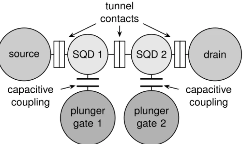
gate voltages, giving the freedom to transition the system from a large SQD to two separated QDs.
source SQD 1 SQD 2 drain
plunger gate 1
plunger gate 2 tunnel
contacts
capacitive coupling
capacitive coupling
Figure 2.8. – A schematic illustration of two SQDs connected in series via tunnel contacts forming a DQD. The two separate plunger gates ideally act only capacitively on the corresponding QD.
Fig. 2.9 shows the transport current through a serial DQD as a function of the plunger gates of the two QDs for a variation of the inter-dot tunnel coupling. In Fig. 2.9 f the coupling is very large, with the conductance resonances showing one set of parallel lines characteristic for a SQD. Two sets of parallel lines emerge for decreasing tunnel couplings of Fig. 2.9 c-d, indicating the formation of a DQD system, with each set of lines representing the conductance resonances of the individual QDs.
For even smaller tunnel coupling, shown in Fig. 2.9 a and b, transport is allowed only at the configurations, where both chemical potentials of the two QDs are aligned with each other and the reservoirs chemical potentials. The points where current can flow in this regime are commonly referred to as triple points, as the charge state of the system sequentially switches between three configurations.
A similar pattern is expected when a charge sensor is employed for the detection
of the electron occupation, with two sets of parallel lines emerging in the derivative
of the sensor current corresponding to a DQD system.
2.6. Single electron in magnetic field
Figure 2.9. – The current through a DQD as shown in Fig. 2.8 as a function of the plunger gate voltages, here denoted as V g1 and V g2 . The bright values represent a significant current flow, while the dark values indicate a suppressed current flow. The coupling strength increases from A to F. The single set of parallel lines observed in F indicate a SQD. This SQD is split into two separate SQDs forming a DQD when the inter-dot tunnel coupling is decreased by the tuning of a gate voltage, with two sets of parallel lines emerging for a strongly coupled DQD in C-E and triple points being observed for weak inter-dot coupling in A and B. From [53]. Reprinted with permission from AAAS.
2.6. Single electron in magnetic field
We now consider a SQD in Si host material which is occupied by a single electron.
For zero magnetic field, the single particle ground state is two-fold spin-degenerate.
In a non-zero static magnetic field B, the spin-up and -down states |↑i and |↓i split
by the Zeeman energy splitting
2.7. Electric dipole spin resonance using a magnetic field gradient
In the following, we will discuss how a magnetic field gradient can be utilized to manipulate single e − spins in semiconductor heterostructures. One key requirement for this concept of manipulation is the presence of a small magnet, typically referred to as micro- or nanomagnet, that provides a local magnetic field gradient across the region where the electron is confined.
Δ B
┴t
t y
QDΔ B
┴y
QDa
b c
Figure 2.10. – Illustration of artificial spin-orbit coupling: a The QD position y QD as a function of time t . In our device the change in position is induced by a microwave (MW)-pulse applied to a gate near the SQD confining the electron.
b The field component ∆ B ⊥ perpendicular to B ext as a function of y QD . c The oscillating ac magnetic field perpendicular to B ext in the electron’s rest frame.
For EDSR the magnetic field component B ⊥ perpendicular (transversal) to B ~ ext is relevant. Fig. 2.10 a shows as schematic representation of the position of the electron wavefunction center y QD as a function of time t . This oscillating displacement, in our case, is induced by applying an ac electric field to a gate in proximity of the SQD confining the electron. As illustrated in Fig. 2.10 b the transversal magnetic field gradient ∆B ⊥ converts this oscillation in space into an ac magnetic field perpendicular to B ~ ext in the electrons rest frame, with the resulting oscillation shown in Fig. 2.10 c.
This conversion of the electron motion into an ac magnetic field via the artificial spin-
orbit coupling introduced by the local magnetic field gradient is the key component
for all-electrical spin-manipulation in our 28 Si/SiGe spin-qubit device.
2.7. Electric dipole spin resonance using a magnetic field gradient
z
x y
z
x´
y´
|↓⟩
|↑⟩
B
1|Ψ⟩ |Ψ⟩
z
x´
y´
B
1|Ψ⟩
|↓⟩
|↑⟩
|↓⟩
|↑⟩
a b c
Figure 2.11. – Illustration of EDSR on the Bloch sphere with |↓i |↑i as the basis states for | Ψ i = a |↓i + b |↑i ; a, b ∈ C: a The laboratory frame of reference, where | Ψ i precesses around the z -axis with ω L . b The rotating frame of reference with x 0 , y 0 rotating at ω L around the z -axis. The ac magnetic field, shown in Fig. 2.10 c, converts into a stationary field B 1 along the x -axis. c The spin precesses around the B 1 axis, leading to Rabi oscillations.
Yet, for a controlled spin-manipulation it is required to couple resonantly to the electron spin. The spin precesses around B ~ ext with the Larmor frequency
f L = ω L
2 π = gµ B B
h , (2.26)
where g is the electron g-factor, µ B is the Bohr magneton, B is the total magnetic field along the nanomagnet axis and h is the Planck constant.
Fig. 2.11 a shows a representation of the electron wavefunction | Ψ i = a |↓i +
b |↑i ; a , b ∈ C on the Bloch sphere with the qubit basis states |↓i and |↑i located on
the poles of the sphere. In this representation the external magnetic field B ext is
oriented along the z-axis. For any | Ψ i not oriented parallel or anti-parallel to the
z -axis, | Ψ i undergoes a precession around the z -axis at a frequency of ω L = gµ ~
BB .
Fig. 2.11 b shows the reference frame rotating at ω L indicated by the rotating basis
vectors x 0 and y 0 . The electron is in the ground state | Ψ i = |↓i represented by the
black arrow. The gray arrow represents the effective magnetic field B 1 created by
3. Gating of undoped Si/SiGe 2DEG
In this chapter, we will discuss the solid-source MBE of the undoped Si/SiGe heterostructures used as the basis for all devices studied in the rest of the thesis.
The charge carrier accumulation in these undoped structures will be demonstrated, followed by a characterization in the form of a magnetotransport study. We will focus on the behavior of Hall bar samples when a bias voltage is applied to the accumulation gate during the cool-down and how the sample characteristics change under illumination at cryogenic temperatures. In particular, we will discuss a previously proposed model [40, 54] based on interface trap states to explain the observed illumination behavior.
3.1. Growth and semiconductor layer structure
3.1.1. Molecular beam epitaxy
The Si/SiGe heterostructures used for the studies in this thesis were grown by
means of solid source MBE based on recipes described in [38–40]. In Fig. 3.1 a the
epitaxy chamber is schematically depicted. There are electron beam evaporator
sources equipped with single-crystalline natural silicon and germanium, labeled Si
and Ge, respectively. A smaller electron beam single-crystalline source equipped with
single-crystalline isotopically purified 28 Si is located at the side of the chamber. The
source crystal for 28 Si, provided by the Leibniz-Institut für Kristallzüchtung (IKZ) in
Berlin, is purified to a residual concentration below 60 ppm 29 Si [34, 35]. The wafer,
onto which the heterostructure is grown, is attached to the temperature-controlled
manipulator
wafer
a b
28
Si
Si Ge Ge content
z
x (001) Si substrate
Si cap Si Ge spacer
1-x xSi quantum well const. composition Si Ge (virtual subst.)
1-x xSi buffer (smoothing) graded buffer (virtual substrate)
Figure 3.1. – a Schematic representation of the MBE ultra high vacuum
chamber, including the source cells for Si, Ge and 28 Si. The wafer, colored
black, is attached to the temperature controlled manipulator. b Illustration of
a typical undoped Si/SiGe layer structure. The Ge content through the layer
structure is indicated by the graph on the right and additionally by the tone of
the background, with a light gray corresponding to a low Ge content while a
dark gray represents a higher Ge content. The Ge content is linearly increased
in the graded buffer layer.
3.1. Growth and semiconductor layer structure
content. Therefore, while the relaxation of the lattice is promoted, the dislocation density at the top of the graded buffer is reduced compared to other buffer concepts such as low temperature Si [38]. This graded buffer is followed by a layer of relaxed constant composition SiGe, completing the part of the heterostructure denoted as virtual substrate (VS) in Fig. 3.1 b. A strained Si QW is grown onto the VS. Either natural Si or 28 Si were employed as a QW material in this thesis. A SiGe spacer is grown to keep the QW away from the heterostructure surface, in order to reduce the scattering potential of defects for a 2DEG in the QW. Finally, a Si cap is employed to create a more stable natural oxide, compared to oxidized SiGe. A chemically stable surface protects the 2DEG properties from deterioration over time.
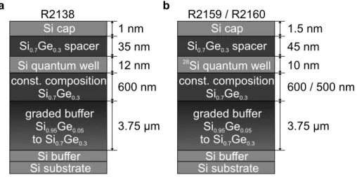
Fig. 3.2 gives a schematic representation of the two layer structures used for all Hall bar samples and QD devices studied in this thesis. Here, Fig. 3.2 a shows a natural Si QW structure with a 35 nm Si 0.7 Ge 0.3 spacer and a 1 nm Si cap and Fig. 3.2 b shows an isotopically purified 28 Si QW structure with a 45 nm Si 0.7 Ge 0.3 spacer and a 1.5 nm Si cap.
3.1.2. Post-growth processing
In further ex-situ processing, outside of the ultra high vacuum of the MBE, the ohmic contact to the QW is created by implantation of high energy ions and a rapid thermal activation anneal at a temperature of 700 ◦ C for 30 s, both performed in the group of Kentarou Sawano (Advanced Research Laboratories, Tokyo City University, Tokyo, Japan). An Al 2 O 3 gate oxide is applied by atomic layer deposition (ALD) at 300 ◦ C.
We employ a post-ALD anneal at 350 ◦ C for 15 min in a forming gas environment (10% H 2 90% N 2 ). The bond pads for the ohmic contacts and the metallic gates are
patterned by lithography and metallization in a standard evaporation chamber.
3.75 µm 600 nm 12 nm 35 nm 1 nm
R2138 R2159 / R2160
3.75 µm 600 / 500 nm 10 nm 45 nm 1.5 nm Si Ge µspacer
0.7 0.3Si Ge
0.7 0.3a b
Si substrate Si cap Si Ge spacer
0.7 0.3Si quantum well const. composition
Si Ge
0.7 0.3Si buffer graded buffer
Si
0.95Ge
0.05to Si Ge
0.7 0.3Si substrate Si cap Si Ge spacer
0.7 0.328
Si quantum well const. composition
Si Ge
0.7 0.3Si buffer graded buffer
Si
0.95Ge
0.05to Si Ge
0.7 0.3Figure 3.2. – Layer structures with the layer thicknesses noted on the right:
a A natural Si QW with 35 nm Si 0.7 Ge 0.3 spacer and 1 nm Si cap (R2138). b A
28 Si QW with 45 nm Si 0.7 Ge 0.3 spacer and 1.5 nm Si cap (R2159 and R2160).
3.2. Hall measurement
In this section, we present the methods for the characterization of the Si/SiGe heterostructures studied in this thesis. We start with an overview of the Hall bar sample layout employed to access important heterostructure properties. We will proceed with a short description of the electrical magnetotransport measurement used for the determination of the charge carrier density and mobility throughout this chapter.
3.2.1. Hall bar sample layout
As shown in Fig. 3.3 a, we fabricate gate-induced Hall bars with the accumulation
gate depicted in light gray. This gate is employed to induce charge carriers forming
a 2DEG in the QW via the field effect. The Hall bar borders are given by the
regions where the field induced by the gate is too weak to induce charge carriers in
the QW. The individual Hall bar segments have a width-to-length ratio of W L = 15 1
with W = 20 µm and L = 300 µm. The QW is contacted by ion-implanted regions,
shown in dark gray in Fig. 3.3 a. An etched bar, indicated by the arrow in Fig. 3.3 a,
prevents a leakage current from the accumulation gate bond pad (labeled 2) into the
active Hall bar region which has occasionally been observed experimentally.
3.2. Hall measurement
L W 18
17
16 15
14 13
3 4
5 6
7 9 1 2
10
a b
V
ag(V)
I (nA)
0 0.5 1
50 40 30 20 10 0
Figure 3.3. – a Hall bar sample layout, with implanted regions in dark gray,
accumulation gate in light gray and an etched leakage current block marked
by the arrow. The contact numbers which we will refer to in this chapter are
indicated in white. b Current through a Hall bar sample as a function of the
accumulation gate voltage V ag . A significant current flows when a threshold
voltage V thr is reached. The maximum current through the sample is limited
to 50 nA by a 100 MΩ resistor. The arrow marks the negative current feature,
attributed to a non-linear I-V curve.
3.2.2. Accumulation of charge carriers in undoped Si/SiGe
Using a standard low-frequency lock-in technique, we measure the current through the sample as well as the longitudinal and Hall voltages in a four-point geometry for one or more segments of the gate-induced Hall bar. For details on the measurement setup, see A.2.1. This allows us to calculate ρ xx and ρ xy , the longitudinal and transversal resistivities, using the width-to-length ratio of the Hall bar following the Eqs. 2.2 and 2.3 in Sec. 2.3.
Fig. 3.3 b shows the current flowing through a typical Hall bar sample while increasing the accumulation gate voltage V ag from 0 V to 1 V. We limit the maximum current flowing through the sample to 50 nA by a 100 MΩ series resistor to prevent damaging of the sample by resistive heating. In the regime of 0 V ≤ V ag ≤ 0.5 V there is no significant current flow through the sample, which we attribute to the energy of the first 2D subband ( E 1st sb ) in the QW still lying above the Fermi energy ( E F ). At about V ag = 0.5 V, marked by the arrow in Fig. 3.3 b, we observe a negative current which is a measurement artifact, explained by a non-linear I-V curve exhibited for low densities of charge carriers in the QW causing a rectification of AC noise signals [55].
With increasing V ag E 1st sb in the QW gets shifted below E F . The current through the sample approaches 50 nA, as the 2D charge carrier density in the QW ( n QW ) increases, as a result of the capacitive coupling of the accumulation gate to the QW.
V ag thus is a tuning knob for the charge carrier density, which will be used to conduct the studies presented in the following sections.
3.2.3. Magnetotransport characterization
An exemplary magnetotransport measurement on the sample R2160A8 for a constant
V ag = 1.1 V is shown in Fig. 3.4, where we plot ρ xx and ρ xy as a function of the external
magnetic field B pointing in out-of-plane direction. For low magnetic fields, ρ xy shows
a linear behavior. The slope of ρ xy allows the determination of the type and density
of charge carriers via the theory of the classical Hall effect. As intended, we find the
charge carriers to be electrons, with a density of n = 5.8 × 10 11 cm −2 according to
Eq. 2.5. Additionally, using the ρ xx value for B = 0 T and Eq. 2.4, the mobility of
the charge carriers may be extracted to a value of µ = 1.1 × 10 5 cm 2 V −1 s −1 . The
mobility is a measure for the scattering of electrons during their transport through
the segment under test. Apart from the classical Hall effect, we observe plateaus in
ρ xy at even filling factors indicated by the dotted lines in Fig. 3.4 and Shubnikov-de
Haas (SdH) oscillations in ρ xx for B > 1 T. These are features of a 2DEG which is
3.2. Hall measurement
B (T)
ρ (Ω)
xxρ (kΩ)
xy0 0.5 1 1.5 2 2.5 3 3.5 4 4.5 5
240 220 200 180 160 140 120
100 0
1 2 3 4 5 6 7
12 10 8 6
Figure 3.4. – Exemplary magnetotransport measurement on a sample with 28 Si QW and 20 nm of Al 2 O x (R2160A8). The longitudinal resistivity ρ xx , plotted in blue as a function of the magnetic field B , shows Shubnikov-de Haas oscillations indicating a well defined 2DEG. The transverse resistivity ρ xy , plotted in red as a function of B, shows a linear behaviour for low magnetic field strengths.
Quantum Hall plateaus are observed for even filling factors indicating a twofold
degeneracy in this measurement.
well described by the theory of the integer quantum Hall effect. The SdH oscillations allow for a separate determination of the charge carrier density, only taking into account charge carriers in the 2DEG. Due to the comparatively larger effective e − mass, in contrast to for example the extensively studied GaAs material system, only a few SdH oscillations are observed in our samples in the accessible magnetic field range of B < 5 T. These few oscillations render the determination of the charge carrier density error prone. Therefore, the charge carrier densities presented in this thesis are solely extracted from the classical Hall effect.
3.3. Introduction to the gating regimes of undoped Si/SiGe
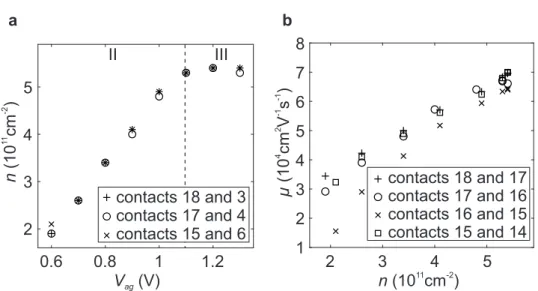
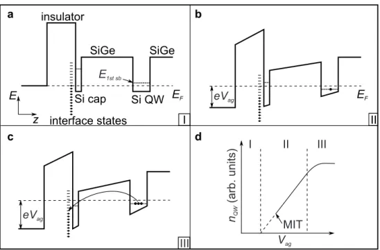
In Fig. 3.5 a the electron density n is plotted as a function of V ag for a Hall bar sample produced from a piece of the wafer R2159 ( 28 Si QW, see Fig. 3.2 b). Note that three different sample positions are plotted. The legend indicates the contact numbers used for the measurements as introduced in Fig. 3.3 a. The charge carrier density rises linearly with increasing V ag in the regime labeled II in Fig. 3.5 a, until the saturation regime, labeled III, is reached for V ag > 1.1 V. The linear increase in charge carrier density in regime II is in perfect agreement with a simple plate capacitor model, with the plates being represented by the accumulation gate and the 2DEG [40, 54, 56]. Based on a previously introduced phenomenological model [40], we attribute the saturation to a charge transfer process from the QW to trap states at the semiconductor-insulator interface. As the densities for all contact pairs coincide, we conclude that the density is constant across the 4 × 5 mm 2 sample for a given V ag . This behavior is representative for all Hall bar samples ( ∼ 10) studied in the course of this thesis.
In Fig. 3.6 a-c we give a schematic representation of the conduction band structure
for the three regimes proposed in the model, labeled I to III. Fig. 3.6 d shows a
sketch of the charge carrier density as a function of V ag with the regimes separated
by the dashed lines. Fig. 3.6 a represents the starting condition for a sample cooled
to 1.5 K with a cool-down voltage V cd = 0 V applied to the accumulation gate during
cool-down. We sketch the conduction band edge as a function of the z-coordinate
(growth direction of the heterostructure). The strained Si-material of the QW and
the Si cap form the minima of the conduction band in the heterostructure. Since the
heterostructure is undoped, there is no inherent band bending and the ground state
energy for electrons in the conduction band E 1st sb , indicated by the dotted line in
3.3. Introduction to the gating regimes of undoped Si/SiGe
V
ag(V)
11-2
n (10 cm )
42-1-1µ (10 cm V s )
11 -2
n (10 cm )
0.6 0.8 1 1.2
2 3 4 5
a b
II III
contacts 18 and 3 contacts 17 and 4 contacts 15 and 6
2 3 4 5
2 3 4
1 5 6 7 8
contacts 18 and 17 contacts 17 and 16 contacts 16 and 15 contacts 15 and 14
Figure 3.5. – a Charge carrier densities n extracted at three contact pairs via the classical Hall effect theory as a function of the accumulation gate voltage V ag . A sample with 28 Si QW and 20 nm of Al 2 O x (R2159A4) was used for this measurement. A linear regime is observed for V ag ≤ 1.1 V where the charge carrier density in the QW may be described by a classical capacitance model (labeled II).
For V ag > 1.1 V we observe a saturation attributed to a charge reconfiguration
into the semiconductor-insulator interface (labeled III). b Mobilities µ as a
function of n calculated for four segments along the sample. The mobility rises
with increasing n due to self-screening. The segment with contacts 16 and 15
shows a lower mobility compared to the other segments, which is found to be
caused by an imperfection in the sample fabrication present in multiple samples.
Fig. 3.6 a, in the QW is above E F , indicated by the dashed line. E 1st sb in the thin Si cap (1-1.5 nm) lies higher than in the QW (10 nm). Considering the phenomenological model previously developed in our group [40, 54], we assume trap states to be present in the vicinity of the semiconductor-insulator interface. In our model, these states are initially filled up to E F when cooled-down from room temperature. Raising the accumulation voltage V ag decreases the potential of the accumulation gate in this picture, leading to a band bending analogous to the operation principle of a field effect transistor and lowering E 1st sb in the QW with respect to E F . We define regime I for all V ag for which in the QW E 1st sb >E F and therefore with no charge carrier density accumulated in the QW. With a more positive V ag , it is possible to bend the band structure in a way that E 1st sb ≤E F as sketched in Fig. 3.6 b. A non-zero charge carrier density is accumulated, with the density depending on V ag as well as on the thickness and dielectric constants of the material between the QW and the accumulation gate, according to a simple parallel plate capacitor model. We define regime II for all V ag where the n QW shows a linear dependence on V ag . In this regime, V ag serves as a tuning knob for the charge carrier density in the undoped Si/SiGe heterostructures studied in this thesis.
As indicated by the arrow in Fig. 3.6 d, the metal-insulator transition (MIT) is crossed in regime II for E 1st sb ≈E F . The values for the charge carrier density at the MIT observed for samples studied in this thesis in the order of 2 × 10 −11 cm −2 (com- pare Fig. 3.5) do match quite well with the theoretical predictions of 1.6 × 10 −11 cm −2 for similar undoped Si/SiGe heterostructures [57].
We observe a distinct transition from the linear regime II to a saturation of n QW
above a certain V ag = V sat , defined as regime III. The constant density for V ag ≥ V sat
is further referred to as saturation density ( n sat ). Based on the phenomenological
model [40, 54], we attribute this saturation to a charge transfer from the QW to the
interface trap states which are energetically available, as sketched in Fig. 3.6 c. The
charge transfer has been found to be independent of the SiGe spacer thickness in
previous results from our group where n sat did not change significantly for a variation
in the spacer thickness [40]. Therefore, we suspect this charge transfer process to
involve Fowler-Nordheim tunneling which is dependent on the strength of the electric
field present between the QW and the accumulation gate but independent on the
thickness of the tunnel barrier [58–60]. One important aspect differs in our model
compared to other models discussed in the literature [59, 60]: our model considers
trap states, while other models incorporate a secondary conduction channel located at
the semiconductor-insulator interface. The absence of a secondary conduction channel
3.3. Introduction to the gating regimes of undoped Si/SiGe
in our structures, is motivated by findings derived from biased-cooling experiments which will be further discussed in 3.4.
In order to investigate the homogeneity of the sample, we turn towards Fig. 3.5 b which shows the mobility calculated for four different segments as a function of the charge carrier density. As expected, the mobility rises for increasing charge carrier densities due to the effect of self-screening [60–62]. One may note, that all but one segment show an identical increase. The lower mobility for the segment between the contacts 16 and 15 was traced back to an imperfection of the lithography mask, as the mobility of this segment was consistently reduced for multiple samples fabricated in the same batch [63]. We conclude that we observe an excellent homogeneity across a single Hall bar sample covering 1.5 mm of active Hall bar region.
Fig. 3.7 shows a log-log plot of the µ vs. n data of contacts 18 and 17 identical to the data shown in Fig. 3.5 b. Assuming a relation of µ ∼ n α [62], we perform a linear regression to the experimental data and find α = 0.79 ± 0.06 for the whole data set with 1.9 × 10 11 cm −2 ≤ n ≤ 5.4 × 10 11 cm −2 with the fit plotted in blue and α = 0.89 ± 0.09 for the low densities: n ≤ 4 × 10 11 cm −2 shown in red. Comparing these exponents with the literature [60–62], we exclude interface-roughness scattering to be the dominant scattering mechanism, as it is predicted that the mobility falls with rising charge carrier density in this case [64], which is not the trend that we observe in our samples. Since the exponents for purely background (scattering centers incorporated due to the finite background pressure during growth) and remote impurity scattering (i.e. impurities at the semiconductor oxide interface further discussed in section 3.4.2) in the strong screening regime are predicted to be
1
2 and 3 2 [62], respectively, it is likely that both of these mechanisms contribute to
the scattering in the studied sample. As this analysis features only one data set, it
would be worthwhile to extend this study to achieve better statistics.
E z
E
Finsulator
Si cap SiGe
Si QW SiGe
interface states I II
a b
c d
E
FeV
ageV
agIII
MIT V
agI II III
n (arb. units)
QWE
1st sbFigure 3.6. – Schematic representation of the conduction band edge energy
as a function of the coordinate in growth direction z draw as a solid line. The
ground state energies of electrons in the Si cap and the Si QW are indicated by
the dotted lines. a Regime I with E 1st sb >E F . b Regime II with E 1st sb ≤E F .
c Regime III with E 1st sb ≤E F and V ag ≥ V sat . The charge transfer from the
QW to the interface trap states is indicated by the arrow. d Sketch of n QW as a
function of V ag with the regimes I to III separated by the dashed lines.
3.4. Biased cool-down
11 -2
n (10 cm )
42-1-1