Angle-Resolved Photoemission Spectroscopy
Boris V. Senkovskiy, 1, 2, ∗ Dmitry Yu. Usachov, 2 Alexander V. Fedorov, 3, 2 Danny Haberer, 4 Niels Ehlen, 1 Felix R. Fischer, 4, 5, 6 and Alexander Gr¨ uneis 1, †
1
II. Physikalisches Institut, Universit¨ at zu K¨ oln, Z¨ ulpicher Straße 77, 50937 K¨ oln, Germany
2
St. Petersburg State University, 7/9 Universitetskaya nab., St. Petersburg, 199034, Russia
3
IFW-Dresden, Dresden, Helmholtzstraße 20, 01069, Germany
4
Department of Chemistry, University of California at Berkeley, Tan Hall 680, Berkeley, CA 94720, United States
5
Materials Science Division, Lawrence Berkeley National Laboratory, Berkeley, California 94720, United States
6
Kavli Energy Nanosciences Institute at the University of California Berkeley and Lawrence Berkeley National Laboratory, Berkeley, California 94720, United States To understand the optical and transport properties of graphene nanoribbons, an unambiguous determination of their electronic band structure is needed. In this work we demonstrate that the photoemission intensity of each valence sub-band, formed due to the quantum confinement in quasi- one-dimensional (1D) graphene nanoribbons, is a peaked function of the two-dimensional (2D) mo- mentum. We resolve the long-standing discrepancy regarding the valence band effective mass (m
∗VB) of armchair graphene nanoribbons with a width of N=7 carbon atoms (7-AGNRs). In particular, angle-resolved photoemission spectroscopy (ARPES) and scanning tunneling spectroscopy report m
∗VB≈ 0.2 and ≈ 0.4 of the free electron mass (m
e), respectively. ARPES mapping in the full 2D momentum space identifies the experimental conditions for obtaining a large intensity for each of the three highest valence 1D sub-bands. Our detail map reveals that previous ARPES experiments have incorrectly assigned the second sub-band as the frontier one. The correct frontier valence sub- band for 7-AGNRs is only visible in a narrow range of emission angles. For this band we obtain an ARPES derived effective mass of 0.4 m
e, a charge carrier velocity in the linear part of the band of 0.63 × 10
6m/s and an energy separation of only ≈ 60 meV to the second sub-band. Our results are of importance not only for the growing research field of graphene nanoribbons but also for the community, which studies quantum confined systems.
I. INTRODUCTION
When a two-dimensional (2D) material is scaled down to a quasi-one-dimensional (1D) ribbon, its electronic structure changes dramatically due to the quantum con- finement of the electron wave functions. Graphene nanoribbons (GNRs) have a band gap and a tunable electronic structure, and therefore they are a promising material for opto-electronic applications. After the dis- covery of bottom-up synthesis which allows atomically precise fabrication, 1 there is a boom in design and study of GNRs. 2–21 The first reported 1 and the most studied system is the semiconducting armchair graphene nanorib- bons of N=7 carbon atoms width (7-AGNRs). The con- ductance of individual 7-AGNRs was measured 22 and the field-effect transistor was fabricated. 23 A wide tunabil- ity of the electronic and optical properties of 7-AGNRs was demonstrated. Particularly, it was shown that the decoupling of 7-AGNRs from the metal substrate af- fects the band gap. 15,24 The 7-AGNRs can be efficiently functionalized by edge groups, 20 by periodically incor- porated boron atoms along the ribbon backbone 6,7 and transformed to a metal by Li-doping. 25 Excitonic effect 3 and defect-induced photoluminescence 16 were observed.
Atomically precise heterojunctions with 7-AGNRs have been also studied. 5,19,26,27 Thus, electronic band struc- ture of this material seems to be well understood.
However, this is not the case. The electronic band
structure of 7-AGNRs consists of 1D sub-bands with
parabolic energy-momentum relation E(k) at the va-
lence band maximum characterized by the effective mass
m ∗ VB = ¯ h 2 (∂ 2 E/∂k 2 ) −1 . The effective mass is an im-
portant parameter characterizing a semiconductor and
there is a large discrepancy in the value of m ∗ VB as
determined by different experimental techniques. Lin-
den et al. 28 demonstrated that the synthesis on a vici-
nal surface Au(788) provides long-range alignment of 7-
AGNRs, since the surface-assisted assembling of the rib-
bons from molecular precursors is confined within nar-
row (≈ 3.8 nm) Au(111) terraces. This alignment al-
lowed to perform first experimental investigation of the
energy band dispersion of 7-AGNRs by means of angle-
resolved photoemission spectroscopy (ARPES). Two va-
lence sub-bands with ≈ 0.3 eV energy separation and
the same effective mass approximately equal to the free
electron mass m e were extracted from the spectra. 28 The
work of Ruffieux et al. 29 demonstrated ARPES measure-
ments of a better quality and revealed three frontier sub-
bands with m ∗ VB ≈ 0.2 m e . Similar energy band dis-
persion was later reported by other authors. 25,30,31 On
another hand, Fourier-transformed scanning tunneling
spectroscopy (FT-STS), where the E(k) is determined
from the interference pattern of the electronic waves re-
flected form the ribbon edges, found m ∗ VB ≈ 0.4 m e . 32
The recent ARPES results of various groups agree to
one another, 25,29–31 making erroneous measurements an
unlikely explanation. The discrepancy between ARPES and STS is quite surprising, since both methods actu- ally should lead to identical results. For example, for 9-AGNRs it was found that ARPES and STS reveal the same value of the effective mass of m ∗ VB ≈ 0.1 m e . 31,33 It is important to understand this issue, since ARPES is a widely used technique to examine the 1D band structure of GNRs 25,28–31,33 and self-assembled poly- meric nanowires. 34–36
The present manuscript resolves this discrepancy by revealing strong anisotropy in the photoemission inten- sity of aligned 7-AGNRs, which makes it impossible to identify all sub-bands in a single ARPES scattering ge- ometry. We demonstrate experimentally, that the pho- toemission matrix element in 1D nanoribbons is a peaked function of the two-dimensional (2D) electron momentum in the ribbon plane. This knowledge allows us to visu- alize the highest three valence sub-bands and determine important parameters for the transport and optical prop- erties, such as effective masses, energy band offsets and the charge carrier velocities. In previous ARPES data the second-highest sub-band of 7-AGNRs was mistakenly considered as the highest one. 25,29–31 Our results high- light that proper application of the ARPES technique for probing the electronic structure of confined systems requires careful consideration of photoemission matrix el- ements.
II. RESULTS AND DISCUSSION
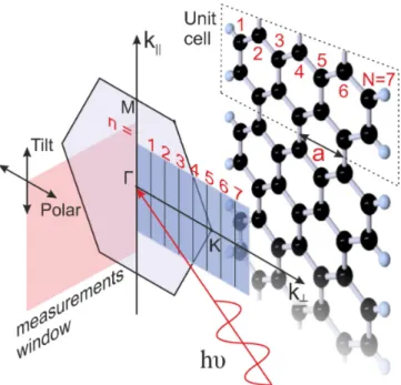
The 1D electronic structure of graphene nanoribbons in tight-binding (TB) model is given by cutting the 2D graphene band structure along confinement lines in mo- mentum space (zone-folding approximation). We intro- duce the parallel (k k ) and the transverse component (k ⊥ ) in the 2D momentum space. Each cutting line at fixed k ⊥
determines the allowed momentum for a N-AGNR and leads to 1D bands below and above the Fermi level with band indices n = 1, . . . N, where N = 7 is the number of atoms along the width of nanoribbon, as it is shown for 7-AGNRs in Fig. 1. ARPES directly reveal energy band dispersion along the defined direction in k-space.
If the ribbons are oriented along the vertical slit of ana- lyzer, the scans will be acquired in some range of k k (Fig.
1). Using the tilt angle one can move the center of the scan along k k , for example, from the Γ (tilt = 0 ◦ ) to the M point of graphene’s BZ, which corresponds to moving from the center of the first to the center of the second 1D BZ of 7-AGNR. By rotating the sample around the polar axis we can change k ⊥ .
Due to quantum confinement the amplitude of the wave function in the direction perpendicular to nanorib- bon axis is changing as sin(q n ⊥ a/2), where q ⊥ n = 2πn
a(N + 1) is the quantized value of k ⊥ and a is the lattice constant of graphene. 37–39 If the final state in the photoemission process is assumed to be a plane wave, then the pho-
toemision matrix element for the π states of GNR in the dipole approximation can be expressed as 31
M (k) ∝ X
j
e −ik
⊥R
j⊥C j (k k ), (1) where R j⊥ are the transverse components of atomic co- ordinates and C j (k k ) are the Bloch wave function am- plitudes for the π states. Here, we neglected the factors related to the photon polarization direction and to the photoionization cross section of 2p z atomic orbitals. The coefficients in Eq. 1 in TB model can be written as 37
C A ∝ sin mq ⊥ n a
2 , C B = ±C A
|f n (k k )|
f n (k k )
, (2) where C A and C B refers to the graphene sub-lattices A and B, ± stands for the conduction and valence bands, correspondingly, m is the number of atomic row along the ribbon width, f n (k k ) = −γ(2e ik
ka/2
√ 3 cos(aq n ⊥ /2) + e −ik
ka/
√ 3 ) and γ ≈ 2.8 eV is the absolute value of the hopping integral. Within TB approximation the sum in Eq. 1 is a Fourier transform of the sine-like wave con- fined along the ribbon width. Therefore, the intensity I(k) ∝ |M (k)| 2 must have strong maxima when the projection of the photoelectron wave vector onto the di- rection perpendicular to the ribbon axis and parallel to the surface matches the values of ±q n ⊥ . It is similar to the momentum quantization in the ARPES spectra of ordered molecular systems. 40–42 The photoemission in- tensity modulation with a change in the emission angle is also well known for the 1D quantum well electronic states confined within nm-scale terraces of stepped noble metal surfaces. 43,44 Substituting the coefficients Eq. 2 in the equation Eq. 1 and taking into account the life time broadening, we can qualitatively describe the photoemis- sion intensity of the valence sub-band n by the following analytical expression
I n (E, k k , k ⊥ ) ∝ β
(E + |f n (k k )|) 2 + β 2
N
X
m=1
e −imk
⊥a/2 sin mq ⊥ n a 2
1 − |f n (k k )|
f n (k k )
2
, (3) where β is the lifetime broadening of bands. The last factor in the sum is related to a phase shift between the wave functions of electrons emitted from the two different sub-lattices and accounts for anisotropic intensity in the ARPES studies of graphene. 45–51
To probe the intensity variation of 1D sub-bands we
set up the ARPES geometry as depicted in Fig. 1. The
Au(788) crystal with aligned ribbons is oriented to mea-
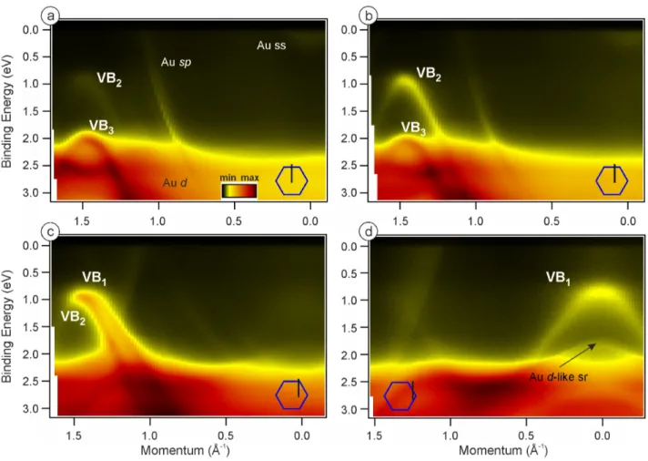
sure the ARPES spectra along the GNR axis. Figure 2
shows the ARPES scans along k k at different k ⊥ , as it
is illustrated in the inset of each panel. We start with
a scan at k ⊥ = 0 ˚ A −1 (Fig. 2 a), that is along the ΓM
direction of the graphene’s BZ, where the parabolic sub-
band VB 3 is observed with the maximal intensity. As we
Figure 1. Sketch of the ARPES experiment and the structure of hydrogen-terminated 7-AGNR with a = 2.46 ˚ A. The cut- ting lines of 7-AGNR inside the unfolded 1D BZ with band indices n = 1, . . . 7 and the 2D BZ of graphene are shown.
The measurements plane is aligned vertically along the rib- bons. The center of the scan is adjusted along k
kby the tilt angle, while k
⊥is changed by the polar angle. The horizon- tally polarized light with a photon energy of 45 eV is utilized.
will show later that is the third 1D sub-band of 7-AGNRs (here we count sub-bands from the Fermi level onwards).
The next sub-band VB 2 is hard to see in this geometry and its intensity rises when we increase k ⊥ (Fig. 2 b). At higher values of k ⊥ (Fig. 2 c), the third sub-band loses its intensity and the highest sub-band VB 1 appears, which determines the VB maximum. This sub-band acquires the intensity in the first 1D BZ when we move the scans along the transverse momentum component further, as it is displayed in the panel (d) of Fig. 2. Thus, the photoe- mission intensity of sub-bands is strongly dependent on k ⊥ . This effect is similar to the intensity oscillations of π-bands of multilayer graphene, where the out-of-plane momentum is quantized. 52
Figure 3 (a) shows the distribution of photoemission intensity in k-space obtained from the TB model us- ing the analytical Eq. 3 at the constant binding energy (1.89 eV). The energy of the valence band maximum in TB calculations is aligned to the experimental energy of VB 1 apex. The orientation of k ⊥ axis is horizontal in ac- cordance with the experimental geometry (Fig. 1). The labeled cutting lines indices n = 5, 6 and 7 of 7-AGNRs (see Fig.1) correspond to the three highest valence sub- bands VB 1 , VB 2 and VB 3 , respectively. Similar picture of the ARPES intensity is obtained with Eq. 1 based on the DFT wave functions of freestanding 7-AGNR (Fig.
3 b). Both theoretical approaches indicate that for each 1D sub-band of 7-AGNR there is a narrow range of k ⊥
where we expect a strong photoemission intensity. Fig- ure 3 (c) shows the experimental constant energy slice of the ARPES map of 7-AGNRs on Au(788), which demon- strates an excellent agreement of the experiment and the theory. In supplementary information we present the theoretical and experimental constant energy cuts of the ARPES map at energies close to the valence band max- imum of 7-AGNRs. The peaked distribution of the pho- toemission intensity for GNRs is different from the case of 2D graphene, where the intensity of π-band changes smoothly in ARPES map around the K point. 46–50
Note that the TB approach is also applicable to the FT-STS measurements and predicts that it is difficult to resolve those sub-bands for which the wave function changes its sign once per unit cell along the ribbon axis. 33 This could be the reason why for 7-AGNRs the second valence sub-band was not visible in FT-STS data. 32
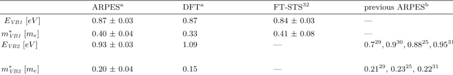
Now we compare the experimental and the calculated band dispersion. Fig. 4 (a) shows the scan, where the two sub-bands VB 2 and VB 3 can be simultaneously ob- served. The black dots indicate the DFT-derived bands with the valence band maximum adjusted to the experi- mental energy of VB 1 . Here we can see qualitative agree- ment in the dispersion of VB 2 and VB 3 for 7-AGNRs on Au with the calculations for freestanding system. How- ever quantitatively there is a difference, particularly, the maximum of VB 2 in experiment is obviously closer to the Fermi level (see Table 1).
Since the first valence sub-band VB 1 is resolved in the first 1D BZ, it can be measured with a tilt = 0 ◦ , as shown in Fig. 4 (b), and its effective mass as well as the en- ergy position of the maximum can be reliably extracted.
The white curve shows the fitting points obtained from the energy distribution curves (EDCs). The highest sub- band can be fitted by a parabola only in the vicinity (≈ 60 meV) of the apex, where we obtain an effective mass of m ∗ VB1 = 0.40 ± 0.04 m e and an energy of E VB1
= 0.87 ± 0.03 eV for the VB maximum. It can be seen in Table 1 that these values are in good agreement with the reported FT-STS data for 7-AGNRs/Au(111). 32 We also found that already at ≈ 250 meV below the max- imum, the dispersion of the first sub-band becomes lin- ear. From the linear slope we extract the charge car- rier velocity v = ¯ h −1 ∂E/∂k k = 0.63 ± 0.05 × 10 6 m/s, which is smaller then the experimental value for free- standing (1.05 × 10 6 m/s) 54 and Au(111) supported (1.2
× 10 6 m/s) 55 graphene, as well as the value determined for the second sub-band of 7-AGNRS in ARPES data (0.82 × 10 6 m/s). 29
The small separation between the first and the second
sub-band of ≈ 60 meV suggests that in the case of hole
doping both of them may play a role in the transport
properties of the material, while the third sub-band is
too low to contribute. This is in a qualitative agreement
with the DFT data, revealing small energy separation
between the two highest valence sub-bands. It should be
noted that the values of the extracted effective masses for
the first and second valence sub-bands are very close to
Figure 2. ARPES scans of 7-AGNRs/Au(788) along k
kat fixed k
⊥= 0 ˚ A
−1(a), 0.3 ˚ A
−1(b), 0.75 ˚ A
−1(c), 1.35 ˚ A
−1(d).
The insets indicate the scan paths (black vertical line) relative to the BZ of graphene. The sequence of the 1D sub-bands of 7-AGNR relative to the Fermi level is VB
1, VB
2and VB
3. The sub-bands with lower energies are not visible because of overlap with the substrate states. The Au sp- and d-states, as well as the surface state (ss) and surface resonance (sr) are marked.
53Figure 3. ARPES intensity at binding energy of 1.89 eV from (a) TB and (b) DFT calculations, (c) experiment. The energy
scale in DFT and TB calculations was rigidly shifted to align the experimental and calculated valence band maxima. The black
and white dashed lines depict the BZs of Au(111) and graphene, correspondingly. The cutting line indices n = 5, 6, 7 derived
from TB approximation and corresponding sub-bands VB
1, VB
2and VB
3are shown. The calculated bands were broadened
with β = 0.1 eV to compare with the experiment.
the values for the corresponding conduction sub-bands obtained from FT-STS measurements, m ∗ CB1 = 0.40 ± 0.18 m e and m ∗ CB2 = 0.20 ± 0.03 m e . 32 Taking into account that theory predicts approximately symmetric band structure for the valence and conduction bands, it also testifies to the validity of our results.
Finally, we would like to address the possible reasons why the frontier sub-band VB 1 was not captured in previ- ous ARPES experiments. As we demonstrated, the full k-space ARPES map of a high resolution is needed to assign the experimentally observed sub-bands of GNRs to the theoretical ones. Here we used hemispherical ana- lyzer with the vertical slit (parallel to the manipulator) to measure scan along the direction of 7-AGNRs alignment and the polar angle to tune k ⊥ . Similar approach can be realized by the analyzer with horizontal slit (most com- monly used in ARPES setups) and GNRs aligned along the slit. Then the tilt or azimuthal angle for mapping in 2D k-space can be used. As it is shown in Fig. 3 and Fig.
2 (a), if one measure strictly along the ribbons axis (k ⊥
= 0) or slightly off (if there is a small deviation in tilt or azimuthal angle for horizontal orientation) the VB 3 and VB 2 should be seen. Indeed, such a picture was ob- served in previous data. 25,29,30 It is intuitive to measure along the ribbon axis, but in this case VB 1 is not visible.
When VB 1 is well observed in the scan, the third sub- band VB 3 loses its intensity (Fig. 3 and Fig. 2 c). Note, that to measure VB 1 in first 1D BZ, as shown in Fig.
2 (d), in horizontal orientation one have to apply large tilt angle (≈ 25 ◦ for photon energy of 45 eV), which de- mands specially designed sample manipulator in ARPES setup. In additional to the experimental configuration, the important issue is the sample itself. Previously, an additional feature was observed in ARPES and taken for the second sub-band VB 2 . 25,29,30 However, this feature is energetically closer to the lowest measured band (VB 3 ) than to the topmost one, while theory predicts relatively small (≈ 0.2 eV) energy separation between VB 2 and VB 1 (see Table 1) and large separation between VB 2 and VB 3 (≈ 1 eV). 1,28 Moreover, as we mentioned above, the- ory and FT-STS data are in good agreement with respect to the conduction sub-bands. 32 Thus, it is unlikely that the observed feature belongs to 7-AGNRs. We suppose that this additional band may be attributed to the elec- tronic states of conjugated 7-AGNRs, particularly N=14 and N=21 AGNRs (two and three fused 7-AGNRs, corre- spondingly). Indeed, when 7-AGNRs are placed close to each other on Au(111) substrate, their wide derivatives at evaluated temperatures 26 or during the long annealing time 19 can be produced. Note, that prior to the ARPES measurements the samples should be degassed by an- nealing after the transfer from ambient conditions. To avoid possible fusion of 7-AGNRs and appearance of ad- ditional bands in our spectra, we synthesized our samples in situ and carefully performed the last step of the syn- thesis (cyclodehydrogenation) of 7-AGNRs on Au(788) at 380 ± 10 ◦ C for 15 minutes.
III. CONCLUSIONS
In summary, we have measured ARPES maps of 7- AGNRs and revealed a strong dependence of photoemis- sion matrix elements for 1D valence sub-bands with re- spect to the experimental geometry. The experimental results together with DFT and tight binding calculations demonstrate that each of the three topmost sub-bands can be selectively visualized by measuring along the rib- bon axis with properly chosen transverse momentum. It is shown that the frontier valence sub-band is very close (≈ 60 meV) to the second one and can be probed in the first BZ of 7-AGNRs, that allows reliable extrac- tion of the effective mass value for the charge carriers in 7-AGNRs of m ∗ VB ≈ 0.4 m e , thus eliminating the old discrepancy between ARPES and STS data. The experi- mental approach used should be also applied for ARPES studies of other types of atomically precise GNRs and nanoribbons of other 2D materials to unambiguously re- veal their band structure, which is a key to electronic and optical properties.
IV. EXPERIMENTAL DETAILS
The measurements have been performed at syn- chrotron HZB BESSY-II at UE112-PGM2 beamline us- ing the 1 2 -ARPES endstation, which is equipped with the 6 axes manipulator and the hemispherical Scienta R8000 analyzer with a vertical slit parallel to the manip- ulator. All spectra are taken at room temperature with p (horizontally) polarized light using the photon energy of 45 eV. During the experiment the base pressure was be- low 2 × 10 −10 mbar. The aligned 7-AGNRs on Au(788) were synthesized in situ using the bottom-up approach. 28
V. THEORETICAL DETAILS
The photoemission intensity was calculated using the dipole approximation for matrix element and the plane wave as a final state. 31 Density-functional-theory (DFT) calculations were carried out using the FPLO-14.00-48 code (improved version of the original FPLO code by Koepernik and Eschrig 56 ) utilizing the generalized gra- dient approximation (GGA) to the exchange-correlation potential. The ribbons were assumed freestanding and hydrogen-terminated. A k-point grid of 12 × 1 × 1 was used to sample the BZ. Atomic positions were relaxed until the forces on each atom were less than 10 −2 eV/˚ A.
ACKNOWLEDGMENTS
B.V.S., A.V.F. and A.G. acknowledge the ERC grant
no. 648589 ’SUPER-2D’, funding from DFG projects
CRC 1238 (project A1) and GR 3708/2-1. D.Yu.U.,
B.V.S. and A.V.F. acknowledge Saint Petersburg State
Figure 4. (a) The valence sub-bands VB
3and VB
2measured in the second BZ of 7-AGNRs along k
kwith k
⊥= 0.2 ˚ A
−1. The black dashed lines show the DFT calculated bands. (b) The frontier valence sub-band VB
1measured in the first BZ of 7-AGNRs along k
kwith k
⊥= 1.5 ˚ A
−1. The white curve indicates the fitting of the EDCs.
Table I. Energies of the band maxima regarding to the Fermi level and the effective masses for the first (VB1) and the second (VB2) valence sub-bands of 7-AGNRs on Au(111) or Au(788).
ARPES
aDFT
aFT-STS
32previous ARPES
bE
VB1[eV ] 0.87 ± 0.03 0.87 0.84 ± 0.03 —
m
∗VB1[m
e] 0.40 ± 0.04 0.33 0.41 ± 0.08 —
E
VB2[eV ] 0.93 ± 0.03 1.09 — 0.7
29, 0.9
30, 0.88
25, 0.95
31m
∗VB2[m
e] 0.20 ± 0.04 0.15 — 0.21
29, 0.23
25, 0.22
31a
This work. The binding energy of VB
1in DFT calculations was chosen equal to the experimental value (0.87 eV).
b
We assume that in previous works the second sub-band was erroneously assigned as the first one.
University for research Grant No. 11.65.42.2017. Re- search supported by the U.S. Department of Energy (DOE), Office of Science, Basic Energy Sciences (BES), under Award no. DE-SC0010409 (design, synthesis and characterization of molecular building blocks) and the Center for Energy Efficient Electronics Science NSF Award 0939514 (SPM imaging and spectroscopy). The
research leading to these results has received fund- ing from the European Community’s Seventh Frame- work Programme (FP7/2007-2013) under grant agree- ment n.312284 (CALIPSO). The authors thank HZB BESSY II for the beamtime allocation. This work has been supported by the University of Cologne through the Institutional Strategy of the University of Cologne within the German Excellence Initiative.
∗
senkovskiy@ph2.uni-koeln.de
†
grueneis@ph2.uni-koeln.de
1
Jinming Cai, Pascal Ruffieux, Rached Jaafar, Marco Bieri, Thomas Braun, Stephan Blankenburg, Matthias Muoth, Ari P. Seitsonen, Moussa Saleh, Xinliang Feng, Klaus M¨ ullen, and Roman Fasel. Atomically precise bottom-up fabrication of graphene nanoribbons. Nature, 466(7305):
470–473, 2010.
2
Yen-Chia Chen, Dimas G. de Oteyza, Zahra Pedramrazi, Chen Chen, Felix R. Fischer, and Michael F. Crommie.
Tuning the band gap of graphene nanoribbons synthesized
from molecular precursors. ACS Nano, 7(7):6123–6128,
2013.
3
Richard Denk, Michael Hohage, Peter Zeppenfeld, Jin- ming Cai, Carlo A. Pignedoli, Hajo S¨ ode, Roman Fasel, Xinliang Feng, Klaus M¨ ullen, Shudong Wang, Deborah Prezzi, Andrea Ferretti, Alice Ruini, Elisa Molinari, and Pascal Ruffieux. Exciton-dominated optical response of ultra-narrow graphene nanoribbons. Nat. Commun., 5:
4253, 2014.
4
Jinming Cai, Carlo A. Pignedoli, Leopold Talirz, Pascal Ruffieux, Hajo S¨ ode, Liangbo Liang, Vincent Meunier, Reinhard Berger, Rongjin Li, Xinliang Feng, Klaus M¨ ullen, and Roman Fasel. Graphene nanoribbon heterojunctions.
Nature Nanotech., 9:896–900, 2014.
5
Yen-Chia Chen, Ting Cao, Chen Chen, Zahra Pedramrazi, Danny Haberer, Dimas G. de Oteyza, Felix R. Fischer, Steven G. Louie, and Michael F. Crommie. Molecular bandgap engineering of bottom-up synthesized graphene nanoribbon heterojunctions. Nature Nanotech., 10:156–
160, 2015.
6
Shigeki Kawai, Shohei Saito, Shinichiro Osumi, Shigehiro Yamaguchi, Adam S. Foster, Peter Spijker, and Ernst Meyer. Atomically controlled substitutional boron-doping of graphene nanoribbons. Nat. Commun., 6:8098, 2015.
7
Ryan R. Cloke, Tomas Marangoni, Giang D. Nguyen, Trin- ity Joshi, Daniel J. Rizzo, Christopher Bronner, Ting Cao, Steven G. Louie, Michael F. Crommie, and Felix R. Fis- cher. Site-specific substitutional boron doping of semicon- ducting armchair graphene nanoribbons. J. Am. Chem.
Soc., 137(28):8872–8875, 2015.
8
Timothy H. Vo, U. Gayani E. Perera, Mikhail Shekhirev, Mohammad Mehdi Pour, Donna A. Kunkel, Haidong Lu, Alexei Gruverman, Eli Sutter, Mircea Cotlet, Dmytro Nykypanchuk, Percy Zahl, Axel Enders, Alexander Sinit- skii, and Peter Sutter. Nitrogen-doping induced self- assembly of graphene nanoribbon-based two-dimensional and three-dimensional metamaterials. Nano Lett., 15(9):
5770–5777, 2015.
9
Haiming Zhang, Haiping Lin, Kewei Sun, Long Chen, Yu- lian Zagranyarski, Nabi Aghdassi, Steffen Duhm, Qing Li, Dingyong Zhong, Youyong Li, Klaus M¨ ullen, Harald Fuchs, and Lifeng Chi. On-surface synthesis of rylene-type graphene nanoribbons. J. Am. Chem. Soc., 137(12):4022–
4025, 2015.
10
Amina Kimouche, Mikko M. Ervasti, Robert Drost, Simo Halonen, Ari Harju, Pekka M. Joensuu, Jani Sainio, and Peter Liljeroth. Ultra-narrow metallic armchair graphene nanoribbons. Nat. Commun., 6:10177, 2015.
11
Pascal Ruffieux, Shiyong Wang, Bo Yang andCarlos S` anchez-S` anchez, Jia Liu, Thomas Dienel, Leopold Talirz, Prashant Shinde, Carlo A. Pignedoli, Daniele Passerone, Tim Dumslaff, Xinliang Feng, Klaus M¨ ullen, and Roman Fasel. On-surface synthesis of graphene nanoribbons with zigzag edge topology. Nature, 531(17151):489–492, 2016.
12
Dimas G. de Oteyza, Aran Garc´ıa-Lekue, Manuel Vilas- Varela, N´ estor Merino-D´ıez, Eduard Carbonell-Sanrom` a, Martina Corso, Guillaume Vasseur, Celia Rogero, En- rique Guitin, Jose Ignacio Pascual, J. Enrique Ortega, Yu- taka Wakayama, and Diego Pe˜ na. Substrate-independent growth of atomically precise chiral graphene nanoribbons.
ACS Nano, 10(9):9000–9008, 2016.
13
Leopold Talirz, Pascal Ruffieux, and Roman Fasel. On- surface synthesis of atomically precise graphene nanorib- bons. Adv. Mater., 28(29):6222–6231, 2016.
14
Ivan A. Verzhbitskiy, Marzio De Corato, Alice Ruini, Elisa Molinari, Akimitsu Narita, Yunbin Hu, Matthias G.
Schwab, Matteo Bruna, Duhee Yoon, Silvia Milana, Xin- liang Feng, Klaus M¨ ullen, Andrea C. Ferrari, Cinzia Casir- aghi, and Deborah Prezzi. Raman fingerprints of atomi- cally precise graphene nanoribbons. Nano Lett., 16(6):
3442–3447, 2016.
15
Shiyong Wang, Leopold Talirz, Carlo A. Pignedoli, Xin- liang Feng, Klaus M¨ ullen, Roman Fasel, and Pascal Ruffieux. Giant edge state splitting at atomically precise graphene zigzag edges. Nat. Commun., 7:11507, 2016.
16
B. V. Senkovskiy, M. Pfeiffer, S. K. Alavi, A. Bliesener, J. Zhu, S. Michel, A. V. Fedorov, R. German, D. Her- tel, D. Haberer, L. Petaccia, F. R. Fischer, K. Meerholz, P. H. M. van Loosdrecht, K. Lindfors, and A. Gr¨ uneis.
Making graphene nanoribbons photoluminescent. Nano Lett., 17(7):4029–4037, 2017.
17
Hironobu Hayashi, Junichi Yamaguchi, Hideyuki Jippo, Ryunosuke Hayashi, Naoki Aratani, Mari Ohfuchi, Shin- taro Sato, and Hiroko Yamada. Experimental and theo- retical investigations of surface-assisted graphene nanorib- bon synthesis featuring carbonfluorine bond cleavage. ACS Nano, 11(6):6204–6210, 2017.
18
Meizhuang Liu, Mengxi Liu, Limin She, Zeqi Zha, Jin- liang Pan, Shichao Li, Tao Li, Yangyong He, Zeying Cai, Jiaobing Wang, Yue Zheng, Xiaohui Qiu, and Dingyong Zhong. Graphene-like nanoribbons periodically embedded with four- and eight-membered rings. Nat. Commun., 8:
14924, 2017.
19
Shiyong Wang, Neerav Kharche, Eduardo Costa Gir˜ ao, Xinliang Feng, Klaus M¨ ullen, Vincent Meunier, Roman Fasel, and Pascal Ruffieux. Quantum dots in graphene nanoribbons. Nano Lett., 17(7):4277–4283, 2017.
20
Eduard Carbonell-Sanrom` a, Jeremy Hieulle, Manuel Vilas- Varela, Pedro Brandimarte, Mikel Iraola, Ana Barrag` an, Jingcheng Li, Mikel Abadia, Martina Corso, Daniel Snchez-Portal, Diego Pe˜ na, and Jose Ignacio Pascual. Dop- ing of graphene nanoribbons via functional group edge modification. ACS Nano, 11(7):7355–7361, 2017.
21
Giang D. Nguyen, Hsin-Zon Tsai, Tomas Marangoni Arash A. Omrani, Meng Wu, Daniel J. Rizzo, Griffin F. Rodgers, Ryan R. Cloke, Rebecca A. Durr, Yuki Sakai, Franklin Liou, Andrew S. Aikawa, James R. Chelikowsky, Steven G.
Louie, Felix R. Fischer, and Michael F. Crommie. Atomi- cally precise graphene nanoribbon heterojunctions from a single molecular precursor. Nature Nanotech., 2017.
22
Matthias Koch, Francisco Ample, Christian Joachim, and Leonhard Grill. Voltage-dependent conductance of a single graphene nanoribbon. Nature Nanotech., 7:713717, 2012.
23
Patrick B. Bennett, Zahra Pedramrazi, Ali Madani, Yen- Chia Chen, Dimas G. de Oteyza, Chen Chen, Felix R. Fis- cher, Michael F. Crommie, and Jeffrey Bokor. Bottom-up graphene nanoribbon field-effect transistors. Appl. Phys.
Lett., 103(25):253114, 2013.
24
Okan Deniz, Carlos S´ anchez-S´ anchez, Tim Dumslaff, Xinliang Feng, Akimitsu Narita, Klaus M¨ ullen, Neerav Kharche, Vincent Meunier, Roman Fasel, and Pascal Ruffieux. Revealing the electronic structure of silicon inter- calated armchair graphene nanoribbons by scanning tun- neling spectroscopy. Nano Lett., 17(4):2197–2203, 2017.
25
Boris V. Senkovskiy, Alexander V. Fedorov, Danny Haberer, Mani Farjam, Konstantin A. Simonov, Alexei B.
Preobrajenski, Niels M˚ artensson, Nicolae Atodiresei,
Vasile Caciuc, Stefan Bl¨ ugel, Achim Rosch, Nikolay I. Ver-
bitskiy, Martin Hell, Daniil V. Evtushinsky, Raphael Ger-
man, Tomas Marangoni, Paul H. M. van Loosdrecht, Fe-
lix R. Fischer, and Alexander Gr¨ uneis. Semiconductor- to-metal transition and quasiparticle renormalization in doped graphene nanoribbons. Adv. Electron. Mater., 3 (4):1600490, 2017.
26
Chuanxu Ma, Liangbo Liang, Zhongcan Xiao, Alexan- der A. Puretzky, Kunlun Hong, Wenchang Lu, Vincent Me- unier, J. Bernholc, and An-Ping Li. Seamless staircase elec- trical contact to semiconducting graphene nanoribbons.
Nano Lett., 17(10):6241–6247, 2017.
27
Eduard Carbonell-Sanrom` a, Pedro Brandimarte, Richard Balog, Martina Corso, Shigeki Kawai, Aran Garcia-Lekue, Shohei Saito, Shigehiro Yamaguchi, Ernst Meyer, Daniel Snchez-Portal, and Jose Ignacio Pascual. Quantum dots embedded in graphene nanoribbons by chemical substitu- tion. Nano Letters, 17(1):50–56, 2017.
28
S. Linden, D. Zhong, A. Timmer, N. Aghdassi, J. H.
Franke, H. Zhang, X. Feng, K. M¨ ullen, H. Fuchs, L. Chi, and H. Zacharias. Electronic structure of spatially aligned graphene nanoribbons on au(788). Phys. Rev. Lett., 108:
216801, 2012.
29
Pascal Ruffieux, Jinming Cai, Nicholas C. Plumb, Luc Patthey, Deborah Prezzi, Andrea Ferretti, Elisa Molinari, Xinliang Feng, Klaus M¨ ullen, Carlo A. Pignedoli, and Roman Fasel. Electronic structure of atomically precise graphene nanoribbons. ACS Nano, 6(8):6930–6935, 2012.
30
Konstantin A. Simonov, Nikolay A. Vinogradov, Alexan- der S. Vinogradov, Alexander V. Generalov, Gleb I.
Svirskiy, Attilio A. Cafolla, Nils M˚ artensson, and Alexei B.
Preobrajenski. Effect of electron injection in copper- contacted graphene nanoribbons. Nano Res., 9(9):2735–
2746, 2016.
31
Boris V. Senkovskiy, Danny Haberer, Dmitriy Yu. Usa- chov, Alexander V. Fedorov, Niels Ehlen, Martin Hell, Re- becca Durr A., Felix R. Fischer, and Alexander Gr¨ uneis.
Spectroscopic characterization of n=9 armchair graphene nanoribbons. Phys. Status Solidi RRL, 11(8):1700157, 2017.
32
Hajo S¨ ode, Leopold Talirz, Oliver Gr¨ oning, Carlo Antonio Pignedoli, Reinhard Berger, Xinliang Feng, Klaus M¨ ullen, Roman Fasel, and Pascal Ruffieux. Electronic band dis- persion of graphene nanoribbons via fourier-transformed scanning tunneling spectroscopy. Phys. Rev. B, 91:045429, 2015.
33
Leopold Talirz, Hajo Sde, Tim Dumslaff, Shiyong Wang, Juan Ramon Sanchez-Valencia, Jia Liu, Prashant Shinde, Carlo A. Pignedoli, Liangbo Liang, Vincent Meunier, Nicholas C. Plumb, Ming Shi, Xinliang Feng, Akimitsu Narita, Klaus M¨ ullen, Roman Fasel, and Pascal Ruffieux.
On-surface synthesis and characterization of 9-atom wide armchair graphene nanoribbons. ACS Nano, 11(2):1380–
1388, 2017.
34
Guillaume Vasseur, Yannick Fagot-Revurat, Muriel Sicot, Bertrand Kierren, Luc Moreau, Daniel Malterre, Luis Car- denas, Gianluca Galeotti, Josh Lipton-Duffin, Federico Ro- sei, Marco Di Giovannantonio, Giorgio Contini, Patrick Le Fvre, Franois Bertran, Liangbo Liang, Vincent Meunier, and Dmitrii F. Perepichka. Quasi one-dimensional band dispersion and surface metallization in long-range ordered polymeric wires. Nat. Commun., 7:10235, 2016.
35
Andrea Basagni, Guillaume Vasseur, Carlo A. Pignedoli, Manuel Vilas-Varela, Diego Pea, Louis Nicolas, Lucia Vi- tali, Jorge Lobo-Checa, Dimas G. de Oteyza, Francesco Sedona, Maurizio Casarin, J. Enrique Ortega, and Mauro Sambi. Tunable band alignment with unperturbed carrier
mobility of on-surface synthesized organic semiconducting wires. ACS Nano, 10(2):2644–2651, 2016.
36
Guillaume Vasseur, Mikel Abadia, Luis A. Miccio, Jens Brede, Aran Garcia-Lekue, Dimas G. de Oteyza, Celia Rogero, Jorge Lobo-Checa, and J. Enrique Ortega. Π band dispersion along conjugated organic nanowires synthesized on a metal oxide semiconductor. J. Am. Chem. Soc., 138 (17):5685–5692, 2016.
37
Huaixiu Zheng, Z. F. Wang, Tao Luo, Q. W. Shi, and Jie Chen. Analytical study of electronic structure in armchair graphene nanoribbons. Phys. Rev. B, 75:165414, 2007.
38
Katsunori Wakabayashi, Ken ichi Sasaki, Takeshi Nakan- ishi, and Toshiaki Enoki. Electronic states of graphene nanoribbons and analytical solutions. Sci. Technol. Adv.
Mater., 11(5):054504, 2010.
39
Ken” ichi Sasaki, Katsunori Wakabayashi, and Toshi- aki Enoki. Electron wave function in armchair graphene nanoribbons. J. Phys. Soc. Jpn., 80(4):044710, 2011.
40
G. Koller, S. Berkebile, M. Oehzelt, P. Puschnig, C. Ambrosch-Draxl, F. P. Netzer, and M. G. Ramsey.
Intra- and intermolecular band dispersion in an organic crystal. Science, 317:351–355, 2007.
41
Peter Puschnig, Stephen Berkebile, Alexander J. Flem- ing, Georg Koller, Konstantin Emtsev, Thomas Seyller, John D. Riley, Claudia Ambrosch-Draxl, Falko P. Netzer, and Michael G. Ramsey. Reconstruction of molecular or- bital densities from photoemission data. Science, 326:702–
706, 2009.
42
Peter Puschnig and Daniel L¨ uftner. Simulation of angle- resolved photoemission spectra by approximating the final state by a plane wave: From graphene to polycyclic aro- matic hydrocarbon molecules. J. Electron Spectrosc. Relat.
Phenom., 200(Supplement C):193 – 208, 2015. Special An- niversary Issue: Volume 200.
43
A. Mugarza, A. Mascaraque, V. Repain, S. Rousset, K. N.
Altmann, F. J. Himpsel, Yu. M. Koroteev, E. V. Chulkov, F. J. Garc´ıa de Abajo, and J. E. Ortega. Lateral quan- tum wells at vicinal au(111) studied with angle-resolved photoemission. Phys. Rev. B, 66:245419, 2002.
44
A. Mugarza, J. E. Ortega, F. J. Himpsel, and F. J.
Garc´ıa de Abajo. Measurement of electron wave functions and confining potentials via photoemission. Phys. Rev. B, 67:081404, 2003.
45
Eric L. Shirley, L. J. Terminello, A. Santoni, and F. J.
Himpsel. Brillouin-zone-selection effects in graphite pho- toelectron angular distributions. Phys. Rev. B, 51:13614–
13622, 1995.
46
Aaron Bostwick, Taisuke Ohta, Thomas Seyller, Karsten Horn, and Eli Rotenberg. Quasiparticle dynamics in graphene. Nat. Phys., 3:36–40, 2007.
47
M. Mucha-Kruczy´ nski, O. Tsyplyatyev, A. Grishin, E. Mc- Cann, Vladimir I. Fal’ko, Aaron Bostwick, and Eli Roten- berg. Characterization of graphene through anisotropy of constant-energy maps in angle-resolved photoemission.
Phys. Rev. B, 77:195403, 2008.
48
Isabella Gierz, J¨ urgen Henk, Hartmut H¨ ochst, Christian R.
Ast, and Klaus Kern. Illuminating the dark corridor in graphene: Polarization dependence of angle-resolved pho- toemission spectroscopy on graphene. Phys. Rev. B, 83:
121408, 2011.
49
Y. Liu, G. Bian, T. Miller, and T.-C. Chiang. Visualizing electronic chirality and berry phases in graphene systems using photoemission with circularly polarized light. Phys.
Rev. Lett., 107:166803, 2011.
50
Choongyu Hwang, Cheol-Hwan Park, David A. Siegel, Alexei V. Fedorov, Steven G. Louie, and Alessandra Lan- zara. Direct measurement of quantum phases in graphene via photoemission spectroscopy. Phys. Rev. B, 84:125422, 2011.
51
Sung Won Jung, Woo Jong Shin, Jimin Kim, Luca Mores- chini, Han Woong Yeom, Eli Rotenberg, Aaron Bostwick, and Keun Su Kim. Sublattice interference as the origin of σ band kinks in graphene. Phys. Rev. Lett., 116:186802, 2016.
52
Taisuke Ohta, Aaron Bostwick, J. L. McChesney, Thomas Seyller, Karsten Horn, and Eli Rotenberg. Interlayer inter- action and electronic screening in multilayer graphene in- vestigated with angle-resolved photoemission spectroscopy.
Phys. Rev. Lett., 98:206802, 2007.
53
P. M. Sheverdyaeva, R. Requist, P. Moras, S. K. Ma- hatha, M. Papagno, L. Ferrari, E. Tosatti, and C. Carbone.
Energy-momentum mapping of d-derived au(111) states in a thin film. Phys. Rev. B, 93:035113, 2016.
54
D. C. Elias, R. V. Gorbachev, A. S. Mayorov, S. V. Mo- rozov, A. A. Zhukov, P. Blake, L. A. Ponomarenko, I. V.
Grigorieva, K. S. Novoselov, F. Guinea, and A. K. Geim.
Dirac cones reshaped by interaction effects in suspended graphene. Nat. Phys., 7:701704, 2011.
55
Julia Tesch, Philipp Leicht, Felix Blumenschein, Luca Gragnaniello, Mikhail Fonin, Lukas Eugen Marsoner Steinkasserer, Beate Paulus, Elena Voloshina, and Yuriy Dedkov. Structural and electronic properties of graphene nanoflakes on au(111) and ag(111). Sci. Rep., 6:23439, 2016.
56