Evolution of electronic structure of few-layer phosphorene from angle-resolved photoemission spectroscopy of black phosphorous
N. Ehlen,1,*B. V. Senkovskiy,1A. V. Fedorov,1,2,3A. Perucchi,4P. Di Pietro,4A. Sanna,5 G. Profeta,6L. Petaccia,4and A. Gr¨uneis1,†
1II. Physikalisches Institut, Universit¨at zu K¨oln, Z¨ulpicher Strasse 77, 50937 K¨oln, Germany
2IFW Dresden, P.O. Box 270116, D-01171 Dresden, Germany
3St. Petersburg State University, 198504 St. Petersburg, Russia
4Elettra Sincrotrone Trieste, Strada Statale 14 km 163.5, 34149 Trieste, Italy
5Max-Planck-Institut f¨ur Mikrostrukturphysik, Weinberg 2, D-06120 Halle, Germany
6Department of Physical and Chemical Sciences and SPIN-CNR, University of L’Aquila, Via Vetoio 10, I-67100 Coppito, Italy (Received 16 August 2016; revised manuscript received 11 November 2016; published 7 December 2016)
A complete set of tight-binding parameters for the description of the quasiparticle dispersion relations of black phosphorous (BP) andN-layer phosphorene withN=1. . .∞is presented. The parameters, which describe valence and conduction bands, are fit to angle-resolved photoemission spectroscopy (ARPES) data of pristine and lithium doped BP. We show that zone-folding of the experimental three-dimensional electronic band structure of BP is a simple and intuitive method to obtain the layer-dependent two-dimensional electronic structure of few-layer phosphorene. Zone folding yields the band gap ofN-layer phosphorene in excellent quantitative agreement to experiments andab initiocalculations. A combined analysis of optical absorption and ARPES spectra of pristine and doped BP is used to estimate a value for the exciton binding energy of BP.
DOI:10.1103/PhysRevB.94.245410
I. INTRODUCTION
Black phosphorous (BP) is a layered crystal which was first discovered in 1914 by Bridgman [1]. The availability of large high-quality BP single crystals laid the foundation for the modern study of this material in the early 1980s [2–8].
Black phosphorous is a semiconductor with a moderate direct band gap 0.31–0.35 eV (Ref. [3,9,10]), as found in electrical transport measurements as a function of temperature. The optical gap of BP is reduced with respect to the transport gap to 0.276 eV for the lowest excitonic state and the light polarized along the armchair edge [7]. The quasiparticle (QP) band structure of BP single crystals was also directly measured using angle-resolved photoemission spectroscopy (ARPES) [5,11].
By using variable photon energies from a synchrotron radiation source the electron dispersion perpendicular to the layers was measured indicating a substantial interlayer bandwidth of about 2 eV [6,12].
Recently, the interest in the fundamental physics of BP and its potential application prospectives has been renewed [13–15] after the successful exfoliation of few-layer phos- phorene (Refs. [16,17]). Phosphorene is the two-dimensional allotrope of BP which shows interesting properties sensibly different with respect to the bulk BP. The tunability of the fundamental direct electronic band gap of phosphorene together with its luminescent properties enables its use in devices. In fact, few-layer phosphorene was already suc- cessfully integrated as the active element in a field effect transistor [17], and its electron mobility reaches values up to 1000 cm2V−1s−1 (Ref. [17]) with on-off ratios of 105 (Refs. [18,19]). The fundamental optical gap of few-layer phosphorene is also direct and has been measured using photo-
*ehlen@ph2.uni-koeln.de
†grueneis@ph2.uni-koeln.de
luminescence (PL) [16,20–22] and optical absorption [23]. For monolayer phosphorene, a QP gap of 2.2 eV and an optical gap of 1.3 eV have been found [24]: The difference can be ascribed to the exciton binding energy, which can be as large as 0.9 eV (Ref. [24]).
However, the values of the band gap of both BP and phosphorene must be taken with care as there is a significant temperature dependence in the band gap [22,25,26]: It is increasing with increasing temperature and as such opposite to the behavior typically observed in semiconductors [27]. In addition, it was recently demonstrated that the exciton binding energy depends on the type of substrate due to environmental effects on the dielectric constant [22]. Phosphorene also shows a strong optical anisotropy for light polarization in the two high symmetry directions which is related to the large anisotropy of the electron effective masses [21,23,24,28,29].
From a theoretical point of view, the interest in the physics of phosphorene is enormous and challenging for first-principles theories. Recentab initiocalculations, at the DFT-GGA level, predict BP to be metallic [30] while DFT-PBE finds a gap of 0.04 eV (Ref. [31]), in striking disagreement with experiments. Only at theG0W0level the agreement with experiment is obtained and an appreciable band gap opens: The band gap of BP reports values of 0.1 eV (Refs. [30,32]) and 0.3 eV (Ref. [31]) within the G0W0 approximation [33,34].
Interestingly, the QP band gap of few-layer phosphorene, calculated by theG0W0approximation, is found to decrease as
∼1/N(Nis the number of layers) from 1.5 eV for monolayer phosphorene to 0.3 eV for bulk BP [30,31]. Extending the calculation to GW with the Bethe Salpeter equation (GW- BSE) [31] and the Kubo formula [35], the optical band gap and optical anisotropy were calculated in agreement with photoluminescence (PL) [16,20–22] and optical absorption [23]. Using a semiempirical interlayer coupling model fitted to first principles calculations, the evolution of the band gap from monolayer to bulk was explained by interlayer coupling [36].
However, although the theoretical predictions are in agree- ment with available experimental results, the application of GW approximation to predict the electronic structure of phosphorene, few layer phosphorene, and black phosphorous is highly demanding from a computational point of view and can often hinder the main physical mechanisms in the description of the experimental results. For this reason, the tight-binding approximation, and in particular its semiem- pirical forms, represents an essential theoretical tool which enables us to interpret the experiments [37], construct a low energy description of the band structure to study the model Hamiltonian [38], and represent a starting point for more advanced calculations [39]. The published tight-binding parameters for black phosphorous and phosphorene usually refer to a four-band model of the system [2,30,40] which, however, may not be suitable to understand many phenomena because it is restricted to a limited energy range. Recently the edge states and Landau levels of phosphorene have been calculated using Wannier functions that define a tight-binding Hamiltonian [41], however an easy parametrization for a full Hamiltonian of the system has not yet been given.
The present paper addresses this issue and is organized as follows: In Sec. II we describe the tight-binding model for the description of the band structure of BP and phosphorene, giving the formulas and meaning of parameters. Then, in Sec. III, we report the results of the experimental measure- ments of the band structure of BP by ARPES, including both the valence and conduction band (see below). In this section, we also provide the set of TB parameters which describe the measured band structure. Section IV and Sec.V report the analysis of the temperature and doping dependence of the electronic properties. Section VI deals with few-layer phosphorene and its description by zone folding. In particular we unravel the origin of the 1/N dependence of the optical band gap of few-layer phosphorene as a function of the number of layers. Then, in Sec.VIIwe discuss the results and give our conclusions and perspectives.
II. TIGHT-BINDING DESCRIPTION OF BLACK PHOSPHOROUS
A. Crystal structure and Brillouin zones
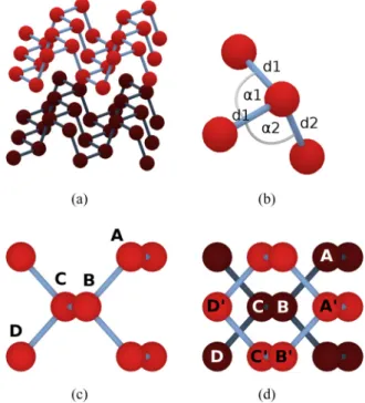
BP is a layered material dominated by covalent bonds for the intralayer bonding and van der Waals forces for the interlayer bonding, similarly to other layered van-der-Waals materials. At variance with graphene, in BP the sp3hybridiza- tion of the 3s, 3px, 3py, and 3pzorbitals leads to the buckled layer structure seen in Fig. 1(a). Under ambient conditions, the stable form of black phosphorus has an orthorhombic crystal structure with lattice and internal parameters reported in TableI.
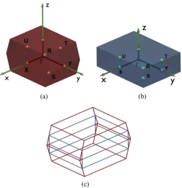
In this paper we will give a TB description of the electronic properties of BP considering the orthorhombic structure with an AB stacking of the layers which is relevant for almost all of the experiments on exfoliated crystals. We use the irreducible body-centered orthorhombic (BCO) cell with four phosphorus atoms for the TB description of BP. For the TB description of N-layer phosphorene through zone folding we will switch to a primitive orthorhombic supercell containing eight phosphorus atoms [see Fig. 1(d)]. The Brillouin zones of the BCOand
FIG. 1. (a) The layered structure of black phosphorous. The colors denote different layers. (b) Bond angles and bond lengths of black phosphorous (see also TableIfor the numerical values). (c) and (d) show the elements in the unit cell of the BCO and the supercell description of BP, respectively.
simple orthorhombic structures as well as their comparison are reported in Figs.2(a),2(b), and2(c).
B. Tight-binding Hamiltonian of black phosphorous For the TB description we use an orthogonal tight-binding model resulting in the Hamiltonian
Hmn(k)=Emδmn+
R=0
eik·Rγmn(R). (1)
Here Em are the on-site energies, and the γmn are hopping parameters withmandnrunning over the orbitals and lattice sites. The electron wave vector is denoted bykand the lattice vectors byR. We employ the Slater Koster scheme forγmn
[43]. This leaves us with four fit parametersVssσ,Vspσ,Vppσ, andVppπ for each order of neighbors that we include in the fit plus the on-site parametersEsandEp. We use the 3s, 3px,
TABLE I. Structural parameters of black phosphorus at room temperature, taken from Ref. [42].
parameter value
d1 2.224 ˚A
bond length
d2 2.244 ˚A
α1 96.34◦
bond angle
α2 102.09◦
a 3.3136 ˚A lattice parameter
b 10.478 ˚A
c 4.3763 ˚A
FIG. 2. (a) shows the Brillouin zone for the BCO description of BP; (b) shows the Brillouin zone of the eight-atom supercell with primitive orthorhombic crystal structure. (c) compares both Brillouin zones in terms of size.
3py, and 3pzorbitals to describe the electron hopping, which results in a 16×16 matrix for the Hamiltonian (four orbitals on four atomic sites in the basis of the BCO description). We end up with a Hamiltonian of the form
H =
⎛
⎜⎝
AA AB AC AD BA BB BC BD CA CB CC CD DA DB DC DD
⎞
⎟⎠, (2)
with each entry αβ, α,β∈ {A,B,C,D} itself being a 4×4 matrix to describe the hopping between the four orbitals centered at sitesαandβ. Taking the symmetries of the lattice into account, we can simplify Eq. (2) to
H =
⎛
⎜⎜
⎝
AA AB AC AD
AB† AA BC AC AC† BC† AA AB AD† AC† AB† AA
⎞
⎟⎟
⎠. (3)
In general, a 4×4 elementαβof the Hamiltonian can be expressed as
αβj,o=
⎛
⎜⎜
⎝
sβ px,β py,β pz,β sα Vssσ,o ljVspσ,o mjVspσ,o njVspσ,o px,α −ljVspσ,o alj,o bljmj,o bljnj,o
py,α −mjVspσ,o bmjlj,o amj,o bmjnj,o
pz,α −njVspσ,o bnjlj,o bnjmj,o anj,o
⎞
⎟⎟
⎠eik·dj,n
with
auj,o =u2jVppσ,o+ 1−u2j Vppπ,o
bsjtj,o =sjtjVppσ,o−sjtjVppπ,o (4) uj,sj,tj ∈ {lj,mj,nj},
where o denotes the order of neighbors and j denotes the corresponding sites on said order. The direction cosines of the direction vector pointing from the site on sublatticeαto sitej on sublatticeβwith neighbor-orderoarelj,mj, andnj. For a given direction vectordj =(dx,dy,dz)Tthey can be computed by
lj =dj,x/||dj||
mj =dj,y/||dj|| (5) nj =dj,z/||dj||.
We can then computeαβas αβ=
o
j
αβj,o. (6)
We fit the TB parameters to describe the experimental (and first-principles) band structure (see below) including any order of neighbors. We find that, in order to describe the
experimental electronic band structure with an accuracy equal to the experimental resolution we need to take into account at least five intralayer and two interlayer matrix elements. Indeed, this is in line with previously published theoretical results [2].
This is, in part, justified noticing that the 6th in-plane and 3rd out-of-plane distances are significantly larger with respect to the previous order (0.5 ˚A and 1.2 ˚A, respectively). In this work however, we chose to include the 6th in-plane order in the model, to capture the effects of the higher in-plane orders (see Sec. III). In order to fit this model to our experimental data (see below), we have extracted the ARPES maxima along the energy dispersion curves (EDCs) and employed a steepest-descent algorithm to minimize the residuals between the theoretical bands and the peaks extracted from the ARPES data along the measured path in the reciprocal space.
III. ANGLE-RESOLVED PHOTOEMISSION MEASUREMENTS OF THE THREE-DIMENSIONAL ELECTRONIC STRUCTURE OF BLACK PHOSPHOROUS
ARPES was performed at the BaDElPh beamline [44] of the Elettra synchrotron in Trieste (Italy) at temperatures of 20 K. This beamline is dedicated to low photon energies and hence higher bulk sensitivity. We used bulk black-phosphorus
crystals from two providers (one from HQ Graphene and one from smart-elements) which gave identical results. The crystal surfaces were preparedin situin a vacuum better than 10−10 mbar by cleaving with a toppost or a scotch tape inside the sample preparation chamber. Immediately after the cleave we determined the high-symmetry directions through low-energy electron diffraction. In order to access both the valence and conduction band of BP, we have performed ARPES on pristine and lithium doped BP. Lithium deposition was carried out in a UHV chamber from SAES getters with the sample at 20 K; the amount of lithium was calibrated by a quartz micro balance.
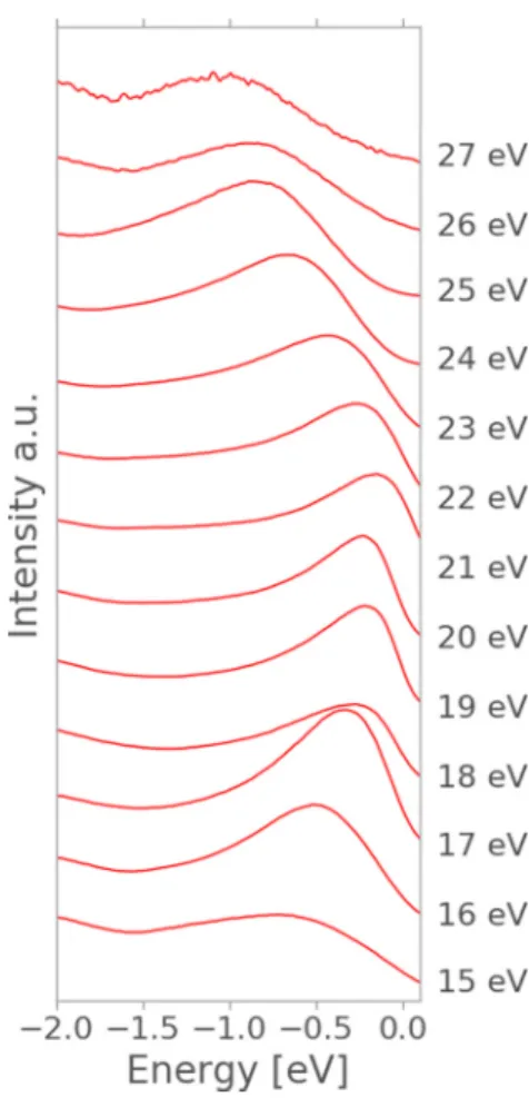
First, we focus on the measured band dispersion starting by looking to the Z dispersion of pristine BP. Since translational symmetry of the crystal potential is broken at the surface, the component of the electron wave vector k which is perpendicular to the layers is notstrictlyconserved in ARPES measurements. However, with the assumptions of a free-electron final state, whose energy depends on an inner potentialV0 (Ref. [45]), we can extract the dispersion of k⊥ inside the material from the measured kinetic energy and angle of the emitted electrons. Assuming that the emitted electrons are excited into parabolalike bands by the incident photons, we can calculate k⊥inside the material by
k⊥ =
2me(Ekincos2θ+V0). (7) We can thus measure the dispersion k⊥ by varying the energy of the incident photon beam. Fig.3depicts EDCs for an in-planek=0. It can be seen that they consist of a single peak which disperses as a function of photon energy. This peak is assigned to the upper valence band of BP. The inner potential is determined by the fact that the top of the valence band is at theZpoint of the BCO Brillouin zone. Fixing the position of the peak to the according position on the Brillouin zone k=(0,0,2π/10.478 ˚A) we have thus assigned the spectrum measured with 21 eV photons to theZpoint. This yields a value for the inner potential ofV0=19.1 eV in very good agreement to previous data [6] which yieldedV0=20.0±0.5 eV. As we will show later, the proper description of the k⊥ dispersion is critically important to understand the band-gap evolution as a function of the number of layers. The ARPES geometry employed for these measurements uses a horizontal slit to collect the photoelectrons. This makes it possible for us to measure theX,Y, ZT, and ZU high-symmetry directions with high resolution in a single scan.
Notably, BP can also be described by a primitive orthorhom- bic unit cell, which being larger than the BCO, would produce backfolding of the valence band and thus a second ”mirrored”
band would be visible in the dispersion. Since this is not the case we confirm that the observed band structure is compatible with the periodicity of the smallest BCO unit cell. We want to underline that we do not observe the additional surface state reported in Refs. [46,47]. Notably, these experiments used photon energies in the range of ∼100 eV. The fact that we do not observe a surface state can be probably attributed to the exceptionally low photon energies we used in our spectra, which are much more bulk sensitive with reduced spectral weight on a surface state.
We now turn to the effect of lithium doping on the electronic structure [32]. Figure4shows an EDC through theZpoint after
FIG. 3. Plot of the energy dispersion curves measured by ARPES fork=0 along theZdirection. The EDC at 21 eV corresponds to k⊥=Z.
lithium deposition. It can be seen that lithium doping raises the Fermi level by about 0.4 eV making the conduction band accessible by ARPES and turning BP into a metal. This effect is not common to all semiconductors, e.g., lithium doping does not induce the metallization of the wide band gap material hexagonal boron nitride [48]. In the present case, the doping
FIG. 4. The EDC corresponding tok=0 andk⊥=Z of the Li-doped BP sample. The lower curve is the EDC with the Shirley background subtracted. The band gap is indicated as the difference between the valence- and conduction-band maxima.
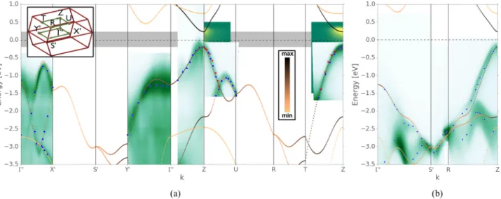
FIG. 5. The ARPES measurements together with the TB fit.•andindicate peaks in the ARPES data of undoped and lithium doped BP, respectively. The color code of the TB calculation represents the pzcharacter of the bands. The inset in (a) depicts a sketch of the BCO BZ with the high symmetry points. The ARPES data of lithium doped BP were up-shifted by a constant energy of 0.32 eV. For this energy shift the valence bands of doped and undoped BP overlap.
induced semiconductor-metal transition is eased by the small band gap of BP.
The doping level we used ensures a rigid shift of the Fermi energy: We verified that the valence band dispersions of pristine and lithium doped BP are identical apart from a constant Fermi level shift (see below). These results are in line with the ARPES spectra obtained with low potassium coverage [49] which also leads to a rigid shift of the band structure [49].
On the contrary, further increasing of potassium doping closes the band gap and can even lead to a band inversion [49].
The shift of the Fermi level across the band gap into the conduction band allows us to extract a value of the “band gap”
from the ARPES data of Fig.4by taking the difference between valence band maximum and conduction band minimum. We obtain a value of 400 meV which is reasonably close to the transport gap of 330 meV [9]. The remaining differences are ascribed to a combination of several effects such as intrinsic doping by impurities, weak interaction with lithium ions, the total energy resolution of the experiment (20 meV), and the fact that the transport gap was extracted by temperature dependent measurements. However, as was shown recently by Villegas and collaborators [50], the band gap has a strong and anomalous temperature dependence which could affect the transport results.
We now move to the in-plane ARPES data shown in Fig.5.
We have taken ARPES scans of the electronic structure along ZUandZTdirections as well as alongXandY (prime in this case denoting the high-symmetry points shifted by a small amount of 0.224 ˚A−1 along thez axis). In order to directly show that doping causes a rigid band shift, we report both the pristine and doped data relative to the Fermi level of doped BP. Applying a rigid band shift of 320 meV to the ARPES data of pristine BP yields a perfect agreement to the valence bands of doped BP. It can be seen that their dispersion is identical apart from the shift in energy due to doping. This corroborates that the doping is in the rigid band shift regime and that the dispersion of the bands are unaffected by the presence of lithium.
Having the complete measured band dispersion of pristine and doped BP we performed the fit of the TB parameters reported in Sec.II. The ARPES spectrum is a renormalized quasiparticle spectrum including many-body effects that are not captured by a simple tight-binding model. For a Fermi- liquid-like doped black phosphorus, the energy scale of these effects should be small compared to our measured energy scale. We find that the TB model describes both the in- plane and out-of-plane dispersions with excellent accuracy.
Moreover, since we included ARPES data of lithium doped BP, we are able to describe also the conduction band close to its minimum. This last result allows us to understand important physical properties of BP and phosphorene which strongly depend on the dispersion of the conduction band: (i) the evolution of the Fermi surface topology of alkali metal doped BP which is predicted to be superconducting [32] and (ii) the dependence of the QP gap of few-layer phosphorene with the number of the layers. The experimental data for the conduction band is limited, not only by the achievable doping levels but
TABLE II. The tight-binding parameters obtained from the fit to the ARPES data. The in-plane and out-of-plane hopping parameters are in units eV.
order Vssσ Vspσ Vppσ Vppπ
1st −5.1008 1.0999 4.2100 −0.6709 2nd −4.5895 3.9570 4.8083 −0.9741 3rd −1.6268 0.6693 1.0361 0.2075 in-plane
4t h −1.1674 0.9023 0.76375 −0.1442 5t h 0.4734 −0.057 0.7221 −0.7869 6t h 5.0773 1.2546 0.3212 −1.0060
1st 0.0848 0.7327 0.6907 0.2313
out-of-plane
2nd −0.6868 0.4964 0.0555 −0.2217 εs −14.6830
on-site
εp −1.5992
FIG. 6. TheoreticalG0W0calculations for the band structure of BP shown in broken blue lines; our TB fit is shown in red. The path through the BZ is the same as for Fig.5(a).
also because high doping levels cause a nonrigid band shift [49].
The set of TB parameters used in the calculation of the band structure reported in Fig. 5is summarized in Table II.
We find that we need to include at least six nearest in-plane neighbors to get a satisfactory fit result. Using a larger number of parameters leads to a smoother decrease of the absolute number of each hopping parameter but does not improve the fit result. Thus, TableIIrepresents an efficient interpolation scheme with a minimum number of parameters.
We also compared the TB band structure with the state-of- the-art ab initiocalculations. In Fig. 6 we report the G0W0 [51] calculation of the bands for bulk BP. In all the relevant regions of the BZ, the agreement between the two sets of bands is reasonably good. In particular the -Z dispersion of the ARPES fit and in theG0W0 calculation has the same features. This indicates that the TB fit of the ARPES data is well suited for the zone-folding approach that we will present in Sec.VI.
IV. TEMPERATURE DEPENDENCE OF THE OPTICAL GAP AND EXCITON BINDING ENERGY
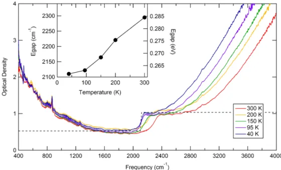
Here we further examine the properties of the band gap of BP by measuring the dependence of the optical band gap as a function of the temperature. Optical absorption measurements were carried out on the same crystal used for ARPES. The measurements were performed using a Bruker 70v spectrometer equipped with a glow-bar source and a DTGS pyroelectric detector. The measured optical density of BP is shown in Fig.7and displays a low frequency absorption that increases for lower wave numbers. It can be described with a Drude term due to the presence of free charge carriers in the range of∼1017cm−3. We speculate that these free carriers are induced by oxygen impurities which would be consistent to the P-O vibration observed at∼880 cm−1[52]. Indeed, DFT calculations have shown that oxygen impurities can donate charge to phosphorene layers [53]. If photons are absorbed across the bandgap of a material, an increase of the optical density is observed at energies which correspond to excitonic and interband transitions [54]. The optical band gap of BP is identified in Fig.7 by a sharp steplike absorption found at 0.261 eV (∼2100 cm−1) at 40 K, in good agreement with previous optical data [7].
It is important to notice that the steplike gap edge highlights the quasi-2D nature of black phosphorus [55]. The smoothing of the step edge can be explained by temperature broadening roughly on the order of kBT which gives a broadening of about 200 cm−1at room temperature, in line with the observed effect.
With increasing temperature the gap edge feature also shifts to higher energies, reaching a value of 0.285 eV at 300 K (see inset of Fig.7). This anomalous temperature dependence has been recently explained considering the coupling of the electrons with low-frequency transverse optical modes [50]. We underline that this same temperature dependence of the gap must also be taken into account when performing temperature-dependent transport measurements to extract the
FIG. 7. Infrared optical density of BP at different temperatures. The optical band gap is extracted by fitting the gap edge with a heavy-side function (dashed line). The inset shows the anomalous temperature dependence of the band gap.
value of the gap [25]. On top of the temperature dependence, the formation of excitons also affects the optical gap. If the optical gapEgap,opticalis purely excitonic, we can estimate the excitonic binding energy by subtracting the optical band gap atT =40 K from the ARPES band gap:
Eexc =Egap,ARPES−Egap,optical≈140 meV. (8) We note, that alternatively to the current approach, there are also purely optical methods for determining the exciton bind- ing energy [54]. These quasiparticle spectroscopy techniques are based on two photon photoabsorption and perform exciton spectroscopy using terahertz light [54].
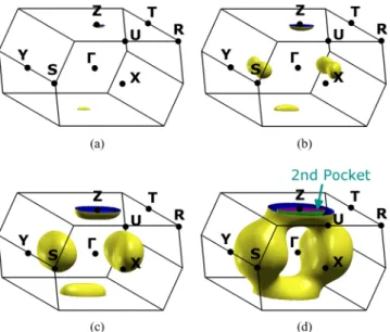
V. DOPING DEPENDENCE OF THE FERMI SURFACE In this section, we examine, using our TB model, the doping dependence of the Fermi surface of BP. The doping dependence of the Fermi surface is relevant for electrostatically gated BP and the description of alkali metal doped BP. The latter has been predicted to become superconducting with experimentally achievable doping levels [32]. The pairing mechanism is thought to be electron-phonon coupling, and the topology of the Fermi surface and the total density of states at the Fermi level have palpable impact on the coupling strength.
In particular, the nesting properties of the Fermi surface can lead to instabilities in the electronic system affecting the lattice dynamics and henceTC. From an experimental point of view, higher doping with respect to the one used in this work may be achieved by liquid ion gating [10] or doping by Ca atoms [56].
Weakly doped BP has only one valley around theZpoint.
However, a close look to the band structures of Fig. 5 and Fig. 6 shows that with higher doping a second valley of the conduction band becomes occupied. The appearance of multiple Fermi surfaces is positive for superconductivity since it would allow us to obtain coupling from a larger set of phonons not only low q-vector optical phonons (intraband scattering) but also highq-vector optical and acoustic phonons
FIG. 8. The Fermi surface of BP in the BCO BZ for doping levels of 50 meV (a), 100 meV (b), 300 meV (c), and 500 meV (d). The appearance of a second pocket is highlighted (see text for discussion).
(mostly via interband scattering). This second valley is located along theY’’ direction in Fig.5. After further doping, shifting the Fermi level of about 0.8 eV with respect to the pristine case, a second conduction subband in the Z point will be occupied. Notably, these predictions come from the TB fit to doped BP but are in excellent agreement to theab initioG0W0 calculations that we showed above in Fig.6.
Figure8 depicts the 3D Fermi surface as it evolves as a function of the doping level (indicated in terms of shifts of the Fermi energy 50 meV, 100 meV, 300 meV, and 500 meV) and calculated by the TB approximation. Figure8(d)shows that at 500 meV electron doping a second electron pocket at theZ point is occupied.
VI. FEW LAYER PHOSPHORENE A. Zone-folding method
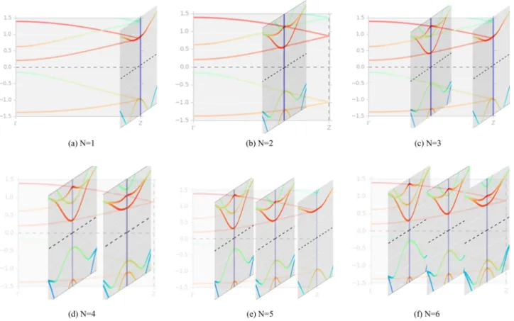
In this section, we apply the zone-folding method to the three-dimensional electronic structure of BP in order to extract the two-dimensional electronic dispersion relations ofN-layer phosphorene. This is of high relevance as the synthesis of few-layer phosphorene in large areas that are needed for ARPES is not feasible up to now. Thus for exploration of the electronic structure of few layer phosphorene, a simple theoretical model is needed. Zone folding is performed in the eight-atom cell depicted in Fig. 2(b) with the electron wave vectorkz perpendicular to the phosphorene layers. In this description the periodicity in thekz direction is halved due to the doubling of the unit cell along thezdirection. This folds back the direct band gap from theZ point of theBCO unit cell to thepoint of the supercell. Modelling theN-layer phosphorene (with the layers located atzi =id,i=1. . . N, with d being the interlayer distance) as infinite potential barriers [located atz=0 andz=(N+1)d] we describe the slab as an infinite potential well in thezdirection, see Fig.9.
Thus, for N-layer phosphorene the electron wave function at the zeroth and the (N+1)th layer must be equal to zero which leads to the following quantization condition for its wavelengthλ:
nλ=(N+1)d, (9)
FIG. 9. Schematic representation of the zone-folding method.
The orthogonal direction can be thought of as a particle-in-a-box model. This leads to a quantization of thekzstates.
FIG. 10. The application of the zone-folding method to BP. Performing cuts at selectedkz,nas given in Eq. (10) yields a set of 2D dispersion relations forNlayer phosphorene. Here we show the dispersion alongZof bulk BP. Cuts perpendicular toZcorrespond to the dispersion relation ofNlayer phosphorene in theYdirection. Plots forN=1. . .6 layered phosphorene are shown. The cuts through the BZ of BP are done increasingly close to thepoint resulting in the reduction of the band gap for higherN.
withnbeing an integer. Depending on whetherN is even or odd, we obtain quantization conditions for kz:
kz,n= nπ
(N+1)d (10)
n=1,2,3, . . . ,N/2 for N even
n=1,2,3, . . . ,(N+1)/2 for N odd. (11) Thus, knowing the experimental band structure of BP, we can describe the electronic structure ofN-layer phosphorene by cuts through the Brillouin zone of bulk BP at thekzvalues allowed by the quantization condition. Figure 10 shows a series of plots highlighting the procedure for N =1. . .6.
ForN layer phosphorene we obtain (N+1)/2 (forN odd) or N/2 (for N even) kz planes in the 3D band dispersion of BP. The value(s) of kz determine the dispersion relation of N layer phosphorene in thekx-ky plane. It can be seen that for monolayer phosphorene, the cut goes through the Z high-symmetry point of the BZ which has the highest separation between valence and conduction bands (in the presently used eight-atom cell). As a consequence, the gap for monolayer phosphorene will be highest when compared to any other layer numberN. For bilayer phosphorene, thekzis located closer to the point, and as a consequence the gap is reduced. This trend holds as we increaseN and the gap is rapidly approaching the bulk value since thekzmove closer towards thepoint according to Eq. (10).
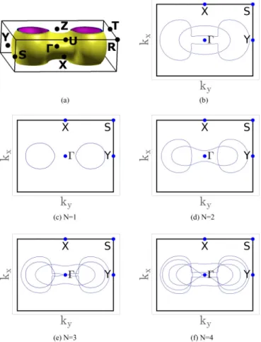
B. Fermi surfaces ofNlayer phosphorene
In the remainder of this section we employ the zone-folding method to calculate the electronic properties of few-layer phosphorene. We start with the layer dependence of the Fermi surfaces of doped few-layer phosphorene which can be obtained by zone folding the Fermi surface of BP in the eight-atom supercell. Figure11(a)shows this Fermi surface at a doping level of 500 meV. It can be seen that, in the plane spanned byZU andZT, the Fermi surface does not cover the volume around theZaxis. However, askzdecreases, the volume around theZ axis becomes occupied. This can be more clearly seen in Fig.11(b)which displays the contours of the Fermi surface from Fig.11(a)atkz=0. Thiskzdependence is important for understanding the layer dependent Fermi surface in N layer phosphorene. Figures 11(c)–11(f) depict the Fermi surfaces ofN=1. . .4 layer phosphorene. A rigid band shift of 500 meV was applied to the zone-folded band structure. It can be seen that the Fermi surface for N =1 consists of pockets in theY direction. ForN 2, another pocket around thepoint appears. Such a layer dependence can affect nesting and might lead to layer number dependence in the superconducting properties, similarly to what is expected for few-layer graphene [57].
C. Energy band gaps ofNlayer phosphorene
We now look in more detail to the valence and conduction band energies ofN layer phosphorene and their dependence
FIG. 11. (a) The Fermi surface of doped BP in the eight-atom supercell for a doping level of 500 meV. (b) Cut through theplane of (a). (c)–(f) The Fermi surfaces for doped 1–4 layer phosphorene.
A doping level of 500 meV has been assumed here, too.
onN. To that end we plot the energies obtained from zone folding as a function ofN in Fig.12.
It can be seen that a family pattern emerges which connects the nth valence (conduction) band energies for differentN.
FIG. 12. Energy eigenvalues at thepoint obtained from zone folding as a function of layer numberN. The blue lines connect the energy eigenvalues of the lowest lying conduction band and the uppermost valence band. A 1/N law that governs the evolution of eigenvalues and a family pattern can be seen.
FIG. 13. The QP and optical band gaps of few-layer phosphorene obtained from zone folding the electronic structure of BP are denoted by
•
. The gap increases when going from bulk BP to monolayer phosphorene. The fit to these data according to Eq. (12) is shown by a solid red line. For comparison we show this work’s results along with previously published theoretical and experimental data ofN-layer phosphorene:: PL (photoluminescence) data from Ref. [20],: PL data from Ref. [21],: PL data from Ref. [16], : QP calculation from Ref. [31],: transport measurements from Ref. [59]. The turquoise line shows the development for the four-band tight-binding model and parameters given in Ref. [60].Notably, similar family patterns have also been observed for few-layer graphene [37,58] where the relevant part of the zone-folded band structure is located along theKH line of the hexagonal BZ. The maximum splitting between the two valence (conduction) bands of graphite is atkz=0 (Kpoint) whereas at the edge of the BZ (H point) the two valence (conduction) bands are degenerate.
Calculating the difference between the lowest conduction band and the highest valence band, which is equal to the QP gap, we compare the QP gap value ofN-layer phosphorene (derived from a fit to ARPES data of doped BP) with the experimental optical and transport band gap of N layer phosphorene of previously published works and theoretical calculations. This comparison is shown in Fig.13. It can be seen that the values of the gap that we obtained from zone folding the band structure of doped BP are in excellent agree- ment toG0W0calculations of few-layer phosphorene [31]. The optical band gaps of few-layer phosphorene as measured by photoluminescence are smaller when compared to the QP band gaps. Despite some scattering in the experimental data, we can observe an increase of the difference between QP gap and optical band gap with decreasing the number of layers. Again, we infer that this trend can be understood as excitonic effects becoming increasingly important for thinner systems. On the other hand, the large variation among individual experiments could perhaps be explained by (1) different environments which have a large effect on the exciton binding energy and (2) different degrees of oxygen exposure which causes doping and hence a change in the optical response.
The dependence of the gapEg(N) on the layer numberN can be fitted by
Eg(N)=1.99e−0.18x
N0.52 +0.41. (12)
FIG. 14. Evolution of the band gap as a function of layer number N is inversely proportional to the number of layers [see Eq. (12)].
The dots show the actual gaps for given values of 1/N; the red line shows an interpolated spline between these values.
This mix of shallow exponential decay andN−a dependence is similar to previous results for a four-band tight-binding Hamiltonian that was fit to GW0calculations [60]. In order to cover a wider range ofN we also show the plot of the band gap as a function of 1/N in Fig.14.
Finally, since zone folding does not capture effects resulting from crystal surfaces, it is interesting to assess the accuracy of zone folding by a comparison of the zone-folded band structure to an explicit TB calculation ofNlayer phosphorene. The cal- culation ofNlayer phosphorene uses an extended Hamiltonian which includes the coupling to adjacent phosphorene layers via the out-of-plane matrix elements. The atoms inside the layers on the two surfaces of the few-layer phosphorene stack will have fewer neighbors to couple to in the extended calculation.
This effect is not included in the zone-folding picture which derives the bands of few-layer phosphorene from the BP.
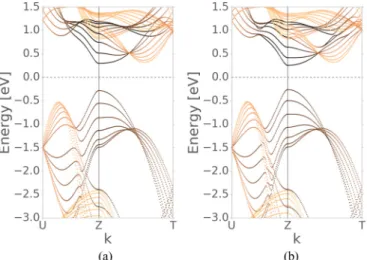
The comparison of the zone-folding result and the extended
FIG. 15. Comparison of the band structure for N=7 layer phosphorene obtained by (a) zonefolding and (b) an explicit tight- binding calculation using an extended Hamiltonian.
calculation is shown in Fig.15. Since black phosphorus is a van der Waals material without dangling bonds, the effects of surfaces are believed to be small, and indeed it can be seen that the zone-folding result agrees well with the explicit calculation ofNlayer phosphorene.
VII. DISCUSSION AND OUTLOOK
ARPES measurements of the three-dimensional electronic structure of BP allowed us to perform a fit of tight-binding parameters of black phosphorus using the Slater-Koster ap- proximation. The experimental data could be described using five in-plane and two out-of-plane neighbor orders. Using this model with our parameters we extract the behavior for the band gap of N-layer phosphorene from the bulk bands using the zone-folding method and find good agreement with calculations and experiments.
Measurements of the optical energy gap indicate that the gap value is close to this separation energy. Moreover the valence band effective mass is not affected by doping in our case, andab initioG0W0 calculations are in agreement with the measured conduction band. From these facts we infer that our doping levels by lithium cause little structural and electronic changes apart from the rigid band shift. The ARPES data of pristine and doped BP are therefore used to fit a new set of tight-binding parameters to the experiment. This accurate set of tight-binding parameters is used to predict a transition into a multiple-valley ground state upon alkali metal doping of BP. Already at experimentally accessible doping levels it is possible to obtain a large Fermi surface area and therefore to take advantage of the full phononic coupling, without relevant momentum restrictions. Most importantly, we employ the zone-folding method to predict the electron energy gap of few-layer phosphorene. The predicted values show the same trend as the experimentally observed energy band gaps of few-layer phosphorene. Finally, the experimental band structure data are compared toab initiocalculations using theG0W0 approximation, and a good agreement is found in most parts of the Brillouin zone. The present work is based on lithium doped BP in the regime of a rigid band shift. It would be interesting to extend it to other alkali or alkaline earth dopants for which effects beyond a rigid band shift could be observed. The proposed tight-binding model can also be useful to describe the electronic structure of gated few-layer phosphorene devices. This would require modifying the on-site tight-binding parameters in a calculation using an extended Hamiltonian of few-layer phosphorene in such a way to model a different charge on each layer.
ACKNOWLEDGMENTS
N.E., B.S., and A.G. acknowledge the ERC Grant No. 648589 ‘SUPER-2D’ and support by DFG through CRC1238 project A1. B.S. and A.G. acknowledge the DFG project GR 3708/2-1. The stay at the Elet- tra synchrotron for ARPES and optical absorption ex- periments has been supported by the CERIC-ERIC consortium.
[1] P. W. Bridgman,J. Am. Chem. Soc.36,1344(1914).
[2] Y. Takao, H. Asahina, and A. Morita,J. Phys. Soc. Jpn.50,3362 (1981).
[3] Y. Maruyama, S. Suzuki, K. Kobayashi, and S. Tanuma,Physica B+C105,99(1981).
[4] S.-i. Narita, S.-i. Terada, S. Mori, K. Muro, Y. Akahama, and S. Endo,J. Phys. Soc. Jpn.52,3544(1983).
[5] T. Takahashi, H. Tokailin, S. Suzuki, T. Sagawa, and I. Shirotani, Phys. Rev. B29,1105(1984).
[6] T. Takahashi, N. Gunasekara, H. Ohsawa, H. Ishii, T. Kinoshita, S. Suzuki, T. Sagawa, H. Kato, T. Miyahara, and I. Shirotani, Phys. Rev. B33,4324(1986).
[7] A. Morita,Appl. Phys. A39,227(1986).
[8] S. Endo, Y. Akahama, S.-i. Terada, and S.-i. Narita,Jpn. J. Appl.
Phys.21,L482(1982).
[9] R. W. Keyes,Phys. Rev.92,580(1953).
[10] Y. Saito and Y. Iwasa,ACS Nano9,3192(2015).
[11] T. Takahashi, H. Tokailin, S. Suzuki, T. Sagawa, and I. Shirotani, J. Phys. C18,825(1985).
[12] L. Liang, J. Wang, W. Lin, B. G. Sumpter, V. Meunier, and M. Pan,Nano Lett.14,6400(2014).
[13] X. Ling, H. Wang, S. Huang, F. Xia, and M. S. Dresselhaus, Proc. Natl. Acad. Sci. USA112,4523(2015).
[14] H. Liu, Y. Du, Y. Deng, and P. D. Ye,Chem. Soc. Rev.44,2732 (2015).
[15] J. Ribeiro-Soares, R. M. Almeida, L. G. Canc¸ado, M. S.
Dresselhaus, and A. Jorio,Phys. Rev. B91,205421(2015).
[16] H. Liu, A. T. Neal, Z. Zhu, Z. Luo, X. Xu, D. Tom´anek, and P. D. Ye,ACS Nano8,4033(2014).
[17] L. Li, Y. Yu, G. J. Ye, Q. Ge, X. Ou, H. Wu, D. Feng, X. H.
Chen, and Y. Zhang,Nat. Nanotechnol.9,372(2014).
[18] S. P. Koenig, R. A. Doganov, H. Schmidt, A. H. Castro Neto, and B. ¨Ozyilmaz,Appl. Phys. Lett.104,103106(2014).
[19] V. Tayari, N. Hemsworth, I. Fakih, A. Favron, E. Gaufres, G.
Gervais, R. Martel, and T. Szkopek, Nat. Commun.6, 7702 (2015).
[20] J. Yang, R. Xu, J. Pei, Y. W. Myint, F. Wang, Z. Wang, S. Zhang, Z. Yu, and Y. Lu,Light. Sci. Appl.4,e312(2015).
[21] S. Zhang, J. Yang, R. Xu, F. Wang, W. Li, M. Ghufran, Y.-W.
Zhang, Z. Yu, G. Zhang, Q. Qin, and Y. Lu,ACS Nano8,9590 (2014).
[22] A. Surrente, A. A. Mitioglu, K. Galkowski, W. Tabis, D. K.
Maude, and P. Plochocka,Phys. Rev. B93,121405(2016).
[23] L. Li, J. Kim, C. Jin, G. Ye, D. Y. Qiu, F. H. da Jornada, Z. Shi, L. Chen, Z. Zhang, F. Yang, K. Watanabe, T. Taniguchi, W. Ren, S. G. Louie, X. Chen, Y. Zhang, and F. Wang,Nat. Nanotech.
(2016), doi:10.1038/nnano.2016.171.
[24] X. Wang, A. M. Jones, K. L. Seyler, V. Tran, Y. Jia, H. Zhao, H.
Wang, L. Yang, X. Xu, and F. Xia,Nat. Nano10,517(2015).
[25] D. Warschauer,J. Appl. Phys.34,1853(1963).
[26] M. Baba, Y. Nakamura, K. Shibata, and A. Morita,Jpn. J. Appl.
Phys.30,L1178(1991).
[27] E. Burstein,Phys. Rev.93,632(1954).
[28] R. Schuster, J. Trinckauf, C. Habenicht, M. Knupfer, and B.
B¨uchner,Phys. Rev. Lett.115,026404(2015).
[29] X. Ling, S. Huang, E. H. Hasdeo, L. Liang, W. M. Parkin, Y.
Tatsumi, A. R. T. Nugraha, A. A. Puretzky, P. M. Das, B. G.
Sumpter, D. B. Geohegan, J. Kong, R. Saito, M. Drndic, V.
Meunier, and M. S. Dresselhaus,Nano Lett.16,2260(2016).
[30] A. N. Rudenko and M. I. Katsnelson,Phys. Rev. B89,201408 (2014).
[31] V. Tran, R. Soklaski, Y. Liang, and L. Yang,Phys. Rev. B89, 235319(2014).
[32] A. Sanna, A. V. Fedorov, N. I. Verbitskiy, J. Fink, C. Krellner, L.
Petaccia, A. Chikina, D. Y. Usachov, A. Gr¨uneis, and G. Profeta, 2D Materials3,025031(2016).
[33] L. Hedin,Phys. Rev.139,A796(1965).
[34] M. S. Hybertsen and S. G. Louie,Phys. Rev. B34,5390(1986).
[35] T. Low, A. S. Rodin, A. Carvalho, Y. Jiang, H. Wang, F. Xia, and A. H. Castro Neto,Phys. Rev. B90,075434(2014).
[36] V. Wang, Y. C. Liu, Y. Kawazoe, and W. T. Geng,J. Phys. Chem.
Lett.6,4876(2015).
[37] A. Gr¨uneis, C. Attaccalite, L. Wirtz, H. Shiozawa, R. Saito, T.
Pichler, and A. Rubio,Phys. Rev. B78,205425(2008).
[38] X.-L. Qi and S.-C. Zhang,Rev. Mod. Phys.83,1057(2011).
[39] E. Cappelluti and G. Profeta, Phys. Rev. B 85, 205436 (2012).
[40] S. Fukuoka, T. Taen, and T. Osada,J. Phys. Soc. Jpn.84,121004 (2015).
[41] J. L. Lado and J. Fern´andez-Rossier, 2D Mater. 3, 035023 (2016).
[42] A. Brown and S. Rundqvist, Acta Crystallogr. 19, 684 (1965).
[43] J. C. Slater and G. F. Koster,Phys. Rev.94,1498(1954).
[44] L. Petaccia, P. Vilmercati, S. Gorovikov, M. Barnaba, A. Bianco, D. Cocco, C. Masciovecchio, and A. Goldoni,Nucl. Instrum.
Methods Phys. Res., Sect. A: Accelerators, Spectrometers, Detectors and Associated Equipment606,780(2009).
[45] A. Damascelli,Phys. Scr.T109,61(2004).
[46] C. Q. Han, M. Y. Yao, X. X. Bai, L. Miao, F. Zhu, D. D. Guan, S. Wang, C. L. Gao, C. Liu, D. Qian, andet al.,Phys. Rev. B 90,085101(2014).
[47] E. Golias, M. Krivenkov, and J. S´anchez-Barriga,Phys. Rev. B 93,075207(2016).
[48] A. Fedorov, C. S. Praveen, N. I. Verbitskiy, D. Haberer, D.
Usachov, D. V. Vyalikh, A. Nefedov, C. W¨oll, L. Petaccia, S.
Piccinin, H. Sachdev, M. Knupfer, B. B¨uchner, S. Fabris, and A. Gr¨uneis,Phys. Rev. B92,125440(2015).
[49] J. Kim, S. S. Baik, S. H. Ryu, Y. Sohn, S. Park, B.-G. Park, J.
Denlinger, Y. Yi, H. J. Choi, and K. S. Kim,Science349,723 (2015).
[50] C. E. P. Villegas, A. R. Rocha, and A. Marini,Nano Lett.16, 5095(2016).
[51] All calculations have been performed at the experimental lattice with the Viennaab initiosimulation package (VASP) [61,62]
and within the generalized gradient approximation [63] (GGA) to density functional theory. We used projected augmented-wave (PAW) [64] pseudopotentials. A cutoff of 300 eV was used for the plane-wave expansion and a 100 eV cutoff for the summation of the response function. BZ sampling has been done with a centered 12×12×8k-point grid.
[52] J. D. Wood, S. A. Wells, D. Jariwala, K.-S. Chen, E. Cho, V. K.
Sangwan, X. Liu, L. J. Lauhon, T. J. Marks, and M. C. Hersam, Nano Lett.14,6964(2014).
[53] A. Ziletti, A. Carvalho, D. K. Campbell, D. F. Coker, and A. H.
Castro Neto,Phys. Rev. Lett.114,046801(2015).
[54] S. W. Koch, M. Kira, G. Khitrova, and H. M. Gibbs,Nat. Mater.
5,523(2006).
[55] M. Dressel and G. Gr¨uner,Electrodynamics of Solids: Optical Properties of Electrons in Matter(Cambridge University Press, 2002).
[56] A. V. Fedorov, N. I. Verbitskiy, D. Haberer, C. Struzzi, L.
Petaccia, D. Usachov, O. Y. Vilkov, D. V. Vyalikh, J. Fink, M.
Knupfer, B. B¨uchner, and A. Gr¨uneis,Nat. Commun.5,4257 (2014).
[57] E. R. Margine, H. Lambert, and F. Giustino,Sci. Rep.6,21414 (2016).
[58] K. F. Mak, M. Y. Sfeir, J. A. Misewich, and T. F. Heinz,Proc.
Natl. Acad. Sci. USA107,14999(2010).
[59] X. Chen, L. Wang, Y. Wu, H. Gao, Y. Wu, G. Qin, Z. Wu, Y.
Han, S. Xu, T. Han, W. Ye, J. Lin, G. Long, Y. He, Y. Cai, W.
Ren, and N. Wang,2D Mater.3,015012(2016).
[60] A. N. Rudenko, S. Yuan, and M. I. Katsnelson,Phys. Rev. B92, 085419(2015).
[61] G. Kresse and J. Furthm¨uller,Phys. Rev. B54,11169(1996).
[62] G. Kresse and J. Furthm¨uller, Comput. Mater. Sci. 6, 15 (1996).
[63] J. P. Perdew, K. Burke, and M. Ernzerhof,Phys. Rev. Lett.77, 3865(1996).
[64] P. E. Bl¨ochl,Phys. Rev. B50,17953(1994).