• Keine Ergebnisse gefunden

PHYSICAL REVIEW B 97, 245402 (2018) Spin-orbit coupling effects in zinc-blende InSb and wurtzite InAs nanowires: Realistic calculations with multiband k · p method

N/A
N/A
Protected

Academic year: 2021

Aktie "PHYSICAL REVIEW B 97, 245402 (2018) Spin-orbit coupling effects in zinc-blende InSb and wurtzite InAs nanowires: Realistic calculations with multiband k · p method"

Copied!
18
0
0

Wird geladen.... (Jetzt Volltext ansehen)

Volltext

(1)

Institute for Theoretical Physics, University of Regensburg, 93040 Regensburg, Germany

3

Institute of Physics, P. J. Šafárik University in Košice, Park Angelinum 9, 04001 Košice, Slovakia

4

Department of Physics, State University of New York at Buffalo, Buffalo, New York 14260, USA

(Received 19 February 2018; revised manuscript received 25 April 2018; published 6 June 2018) A systematic numerical investigation of spin-orbit fields in the conduction bands of III-V semiconductor nanowires is performed. Zinc-blende (ZB) InSb nanowires are considered along [001], [011], and [111] directions, while wurtzite (WZ) InAs nanowires are studied along [0001] and [1010] or [1120] directions. Robust multiband k · p Hamiltonians are solved by using plane-wave expansions of real-space parameters. In all cases, the linear and cubic spin-orbit coupling parameters are extracted for nanowire widths from 30 to 100 nm. Typical spin-orbit energies are on the μeV scale, except for WZ InAs nanowires grown along [1010] or [1120], in which the spin-orbit energy is about meV, largely independent of the wire diameter. Significant spin-orbit coupling is obtained by applying a transverse electric field, causing the Rashba effect. For an electric field of about 4 mV/nm, the obtained spin-orbit energies are about 1 meV for both materials in all investigated growth directions. The most favorable system, in which the spin-orbit effects are maximal, are WZ InAs nanowires grown along [1010] or [1120] since here spin-orbit energies are giant (meV) already in the absence of electric field. The least favorable are InAs WZ nanowires grown along [0001] since here even the electric field does not increase the spin-orbit energies beyond 0.1 meV. The presented results should be useful for investigations of optical orientation, spin transport, weak localization, and superconducting proximity effects in semiconductor nanowires.

DOI: 10.1103/PhysRevB.97.245402 I. INTRODUCTION

The ultimate goal of spintronics is to enhance the functional- ities of electronic devices by exploring the spin degree of free- dom [1,2]. In low-dimensional semiconductor nanostructures, the control of spin allows to transfer information between spin and light [3–7], and can realize topological states of matter [8]

and helical states in one-dimensional (1D) nanowires [9–12]

that are essential in the search for Majorana zero-energy states [9,13]. In particular, semiconductor nanowires with strong spin-orbit coupling (SOC), such as InSb and InAs, in proximity with an s-wave superconductor may support such zero-energy bound edge state, when time-reversal symmetry is broken by a magnetic field [14–19].

In the absence of space-inversion symmetry, in addition to orbital splittings at high-symmetry points and lines, SOC is also manifested by the spin splitting of the energy bands and by the appearance of a spin texture on energy surfaces.

The spin splitting can arise from two main contributions:

the bulk-inversion asymmetry, known as BIA [20], and the structural-inversion asymmetry, known as SIA [21]. The for- mer is present in materials, such as III-V semiconductors, lacking space inversion in the primitive cell. The latter appears due to quantum confinement, at interfaces in heterostructures, and in the presence of an applied electric field. Tuning the interplay between different sources of SOC can lead to per- sistent spin helices [22–24], spin field-effect transistors [25], g-factor anisotropies [26–28], and significant changes in the spin relaxation times [29,30].

Experimentally, reliable determination of the SOC strength in nanowires is a challenging task [31]. Distinct setups yield differing values [30,32,33]. For example, SOC strengths in the same material, extracted from weak antilocalization measure- ments, come out different [34–37]. These distinct values are due to the electron-electron contribution (Hartree potential) to the Rashba SOC term [38–41], i.e., the fields induced by the gates lead to a charge unbalance in the system. This charge unbalance gives rise to the Hartree potential which is strongly dependent on the system configuration and has a large contribution to the Rashba SOC term. Theoretically, it is common to use reduced models for the semiconductor conduction band [1,2,21,42]. In these models, SOC enters as an empirical parameter that can assume a wide range of values for the same system depending on what is measured [30,33,43–45].

Motivated by the hybrid semiconductor-superconductor proposal [9,46] as a platform for the zero-energy Majorana bound states, that uses semiconductor nanowires with large SOC, we investigate the role of BIA and SIA SOC terms in free-standing zinc-blende (ZB) InSb and wurtzite (WZ) InAs nanowires. In particular, we address theoretically how the quantum confinement, given by the nanowire diameter, and the orientation of the nanowire (growth direction) modifies the main parameter, the SOC energy, that defines if the system can (or cannot) host Majorana zero-energy excitations.

Both multiband tight-binding and k · p methods [47–53]

have been successful in the determination of the electronic

and spintronic properties of nanowires. Here, we use robust

(2)

multiband k · p models: a 14-band Kane model [2,54,55] to treat ZB InSb nanowires and 8-band model [56] to treat WZ InAs nanowires, under the envelope function approximation and plane-wave expansion. The BIA SOC for ZB is taken into account with the addition of the extra conduction bands (in comparison with the 8-band model) and their explicit coupling parameters; in the WZ case we also include often neglected linear-in-momentum SOC terms in the 8-band model [57–60].

We also apply an electric field, transverse to the nanowires axes, to investigate the Rashba effect and extract the field-dependent spin-orbit parameters.

We give the essential spin-orbit splitting parameters and effective masses for the lowest conduction subbands, for a set of hexagonal nanowires, from 30 to 100 nm, oriented along different directions: [001], [110], and [111] for ZB InSb, and [0001] and [1010] or [1120] WZ InAs nanowires. In the absence of electric field, the spin-orbit energies of ZB InSb nanowires are tiny, on the order of micro eVs. However, due to the presence of a linear spin-orbit splitting in the bulk, WZ InAs nanowires exhibit giant splittings already in the absence of the field. Although symmetry suppresses the spin-orbit energy for [0001] nanowires, the splitting is about 1 meV in [1010] or [1120] cases.

Under an applied electric field, ZB InSb nanowires can exhibit spin splittings as on the meV scale, in the fields of a few mV/nm. We find that this Rashba effect does not depend essentially on the growth direction, nor on the nanowire diameter. However, the case of WZ InAs nanowires is curious.

The electric field does not significantly increase the spin split- ting for [0001] directions. For example, the spin-orbit energy reaches only 20 μeV for fields of 4 mV/nm, hardly enough to be practical as a platform for topological superconductivity.

This material system is rather unfavorable in this sense. On the other hand, the spin-orbit energy of WZ InAs nanowires grown along [1010] or [1120] retain their meV spin-orbit energies, not being influenced much by the field. We conjecture that this is true even in the presence of gating interfaces, meaning that the bulk effect dominates over the interfaces and electric fields which further reduce space-inversion symmetry. The robustness and large value of the spin-orbit energy in these systems makes us suggest them as favorable systems.

Spin-orbit coupling in semiconductor nanowires has re- cently been investigated. Kammermeier et al. [45] devised a theoretical framework to calculate the weak antilocaliza- tion effects in cylindrical nanowires and have successfully reproduced the values of α R ≈ 0.1–0.3 meV nm for ZB InAs nanowires [61–65]. Winkler et al. [53], using multiband k · p for WZ InAs oriented along [0001] direction and tight-binding model for ZB InSb oriented along [111] direction, found an increase, of one order of magnitude or more, in the g-factor of excited conduction subbands due to the spin-orbit coupling.

Luo et al. [66] found a giant Rashba effect of holes in semi- conductor nanowires. Using an atomistic approach, they found that the hole Rashba coefficient of ZB InAs nanowires under an applied electric field of the order of 0.5 mV/nm is about two to five times larger than the electron Rashba coefficient.

Consistent with our results, they also found a saturation of the electron Rashba coefficient with increasing nanowire diameter.

Moreover, Wójcik et al. [41] using a two-band k · p model (by folding down the 8-band Kane model), in a self-consistent

framework were able to accurately reproduce the results for ZB InSb nanowires from Ref. [36]. Unlike in our work, which provides setup-free spin-orbit parameters, these authors fixed the nanowire diameter and orientation and studied how SOC changes with distinct gate configurations and charge profiles.

Nevertheless, in their calculations they found for a ZB InSb nanowire with L ≈ 100 nm for a fixed chemical potential of 0.2 eV and an applied electric field of 4 mV/nm, a Rashba coefficient of about α R = 2α ≈ 50 meV nm which is in good agreement with our results of α ≈ 19 meV nm. Furthermore, for WZ InAs nanowires oriented along [0001] direction with 100 nm in diameter, the authors in Ref. [17] reported α R = 8 meV nm also in agreement with values reported in Ref. [16], which is about 1.6 times larger than our reported value of 2α ≈ 5 meV nm for a 4 mV/nm applied field, although in both papers it is not clear the value of the applied electric field.

Moreover, the authors in Ref. [67] experimentally detected that for WZ CdSe nanowires the Dresselhaus SOC is absent for nanowires oriented along [0001] direction but present for [1120] direction, which is consistent with our results.

This paper is organized as follows: In Sec. II we present the geometric schematics of the nanowires we have simulated specifying the orientations and coordinate axes. Following, we introduce the respective k · p models we used as well as the numeric procedure employed to calculate the energies and states of the nanowires. After that, in Sec. III, we present the model Hamiltonian including SOC and its energy dispersion.

With the expression from the energy dispersion we then apply a fitting procedure to the lowest conduction subband of the nanowires. In Sec. IV we discuss the specifics of the effective masses and SOC in ZB type structures following, in Secs. IV A–IV C, with a detailed examination of the SOC in the distinct nanowire orientations. In Secs. V and V A and V B we do the same but for WZ crystal phase. Next, in Sec. VI we discuss the essential SOC effects in nanowires from the perspective of finding a topological quantum phase transition in superconducting nanowires. Finally, we conclude in Sec. VII.

II. NANOWIRE MODELING

By carefully controlling growth conditions [68–70], semi-

conductor nanowires using III-V compounds can be synthe-

sized with pure ZB or WZ crystal phases [68], but also

with a mixed phase [71]. Furthermore, it is possible to

obtain nanowires with a variety of cross sections, such as

hexagonal, circular, square, etc., grown along different di-

rections. Typically, ZB nanowires grow along [111] direction

with hexagonal cross section [72–74], while [001] nanowires

have typically square cross section [72,74–76]. As for [110]-

oriented ZB nanowires there can be several cross-section

configurations from trapezoidal to diamondlike shapes and

nonregular hexagons [72,74,77–80]. WZ nanowires can be

typically fabricated along [0001] with hexagonal cross section,

while WZ nanowires grown along [1120] and [1010] present

square cross section [70,74,81]. On the other hand, from

a theoretical perspective nanowires are usually treated with

cylindrical or square cross section, which simplifies the calcu-

lations without sacrificing the underlying physical features of

the system [45,82–84].

(3)

FIG. 1. (a) Schematics of a hexagonal nanowire and the coordi- nate axes we use in the text. The nanowire growth direction is along z, and the electric field is applied along the y direction. The wire diameter is L, which is the distance between the opposite vertices of the hexagon. In (b) and (c) we show the growth planes (shaded regions) inside the conventional unit cells for ZB and WZ crystals, respectively. In (c) the dashed lines represent the primitive unit cell.

The coordinate axes with respect to the crystal orientations are also indicated for [001] ZB and [0001] WZ structures. These are the same axes as used in the confinement geometry (a).

In this paper, we consider ZB InSb and WZ InAs nanowires with hexagonal cross section [85], oriented along different (growth) directions, as shown in Fig. 1. We calculated ZB nanowires oriented along [001], [110], and [111] directions and WZ nanowires oriented along [0001], [1120], and [1010]

directions. The diameter of the nanowires is denoted as L, defined as the largest distance between vertices [see Fig. 1(a)].

Our Cartesian system has its z axis along the growth direction, while the quantum confinement is in the xy plane. For a ZB nanowire grown along [001], this would mean that x is [100], y is [010], and z is [001]. For a WZ nanowire grown along [0001], the hexagonal atomic arrangement is compatible with the hexagonal confinement of the nanowire [see Fig. 1(c)].

For all other orientations, the relation between the Cartesian coordinates and the crystallographic orientations is discussed in the corresponding sections.

Bulk ZB crystals are invariant under T d , and WZ crystals under C 6v symmetry operations. Because space-inversion sym- metry is broken in these two crystal phases, the energy bands of both ZB and WZ nanowires exhibit generic spin split due to the (bulk-inversion) asymmetry. To simulate realistic experimental conditions, we also apply an external electric field in the

The electric field introduces additional spin-orbit splitting, which in general interferes with BIA SOC. The resulting spin-orbit splitting can be said to be due to structure-inversion asymmetry (the Rashba effect), although this terminology is not unique, and we simply refer to the spin-orbit splitting without any labels, but stating the material, confinement geometry, nanowire orientation, and the electric field. Electric field also reduces the mirror symmetry, resulting in further orbital splitting of the conduction band subbands, as shown in Figs. 7, 11, 15, 19, and 23.

In order to calculate the electronic structure of ZB InSb and WZ InAs semiconductor nanowires and extract the spin-orbit splitting of the lowest conduction subbands, we employ the multiband k · p method combined with the envelope function approximation. Our k · p Hamiltonians describe realistically the bulk cases as the reference points.

For ZB InSb we use a 14-band extended Kane model [2,54,86,87]. which provides the relevant SOC features in the lowest conduction band via coupling to higher conduction bands [88]. The involved bands are the lowest s conduction and the lowest three p conduction bands, as well as the three highest p valence bands (heavy and light, and spin-orbit split-off bands). Including the spin degree of freedom to these bands, we end up with a total of 14 bands. We use the parameters [89] for InSb from Ref. [54]. If we took an 8-band model [90,91], with only the lowests conduction subband, we would fail to describe properly the bulk spin-orbit splitting because this model lacks the couplings that generate the bulk spin splitting observed in ZB III-V semiconductors.

For our WZ InAs nanowires we use the 8-band k · p model with k-dependent SOC terms [56], that reproduces very well the bulk SOC features in the vicinity of -point. Such k- dependent terms are usually neglected in conventional 8-band WZ Hamiltonians [93–95], but they are needed to accurately describe bulk spin-orbit effects in WZ InAs [56].

To model quantum confinement, we use the envelope function approximation [96–99]. Essentially, this treatment applied to the multiband k · p Hamiltonians means substituting bulk wave numbers k x(y) by operators − i ∂/∂x(y ), keeping k z a parameter, thus transforming the bulk multiband Hamiltonian into a set of coupled linear differential equations. To solve these coupled differential equations, we employ the plane-wave ex- pansion [95,100–104], that is, the Fourier transform of the real- space-dependent parameters. In narrow-gap semiconductors, real-space treatment of confined systems can lead to spurious solutions and special treatment [49,105,106] should be applied to eliminate them, while using Fourier transformation the spu- rious solutions are easily identifiable and controllable [102].

The plane-wave expansion works by creating, effectively,

periodically repeated systems of nanowires with vacuum in-

between. To treat the vacuum we follow the suggested values,

in Ref. [92], of the band offset for the conduction band as

(4)

va len ce ban ds con d uct ion band s

(a) ZB (b) WZ

FIG. 2. Schematics of the band alignment. (a) ZB 14-band model with band alignment to vacuum. The band-gap energy is E

0

for the s conduction band and E

0

for the p

conduction band. In the valence band,

0

is the the spin-orbit coupling splitting, while in the p

conduction band it is described by the

0

parameter. (b) WZ 8-band model with band alignment to vacuum. The p valence bands have an extra splitting (due to the crystal field) at point, making them only spin (and no longer orbital) degenerate. The energy labels for WZ are also indicated: E

c

is the conduction band minimum, and E

i0

, i = 1, 2, and 3, are the valence band maxima. The conduction bands offset to the vacuum is 5.5 eV, and the valence bands offset is 2.5 eV following Ref. [92].

5.5 eV and for the valence band as 2.5 eV. In Fig. 2, we show a scheme of the used band alignment of the semiconductor with the vacuum. In Appendix A we discuss the plane-wave expansion approach and its numerical implementation.

In addition to confinement, we also apply electric field across the nanowires, along x and y directions [see Fig. 1(a) for the choice of coordinate system]. For example, if the electric field is along y, the voltage drop along the nanowire is

V ele = e E y, (1) where e is the modulus of the electron charge and E is the applied electric field. The values of y range from 0 to L, thus thicker nanowires have larger values of V ele for a fixed value of E. For sufficiently large values of V ele , the confinement profiles of conduction and valence energy bands overlap, therefore closing the gap of the system. In Appendix B we show an example of such case. Although interesting physical phenomena can be found in gapless systems [107,108], in this study we focus on values of electric fields that do not overlap conduction and valence energy band profiles, i.e., we are considering gapped systems.

III. MODEL HAMILTONIANS

We fit our numerical data to effective Hamiltonians in order to extract useful parameters such as effective masses and SOCs.

In general, the conduction bands of our nanowires follow the 2 × 2 Hamiltonian

H = H 0 + H BIA + H SIA . (2) Here, H 0 is the effective mass Hamiltonian, expressing the parabolic dispersion near the point. The remaining two terms express the bulk-inversion (BIA) and structure-inversion

(SIA) asymmetry-induced SOCs. For conduction electrons, which form orbitally nondegenerate bands, these spin-orbit Hamiltonians are conventionally written as

H = ( k) · σ , (3) where k is the spin-orbit field. Time-reversal symmetry requires it to be an odd function of momentum ( k) =

(− k). Otherwise, the functional form of the spin-orbit field is restricted by the crystal and confinement symmetry.

Each structure has its own functional form of the effective mass and spin-orbit field, based on the symmetry. In the following sections, we discuss the specific forms and present effective masses, as well as spin-orbit field parameters up to cubic-in-momentum terms

E = 2(αk + γ k 3 ). (4) Apart from α and γ , an important measure of the strength of SOC is the spin-orbit energy,

E SO = (2 α) 2 m

2 ¯ h 2 , (5)

where m is the effective mass of the conduction band. The spin-orbit energy is indicated in Fig. 3.

Our goal is to provide a reliable fitting of these effective models to the numerical calculations using the multiband k · p Hamiltonians. The fitting procedure is illustrated in Fig. 4.

We fit the lowest conduction band, as calculated with the k · p method, using a cubic fitting, i.e., up to third order in the momentum [see Eq. (4)]. The agreement is in general excellent.

From that fitting we obtain the effective mass of the lowest conduction band. The subband’s spin splitting, induced either by the structure itself or by the applied electric field, is then divided by momentum, providing a nice way of obtaining the linear spin-orbit splitting parameter α as the intersection with the vertical axis. A quadratic fitting to this curve determines the cubic coefficient γ . In Appendix C we discuss the effects of higher conduction subbands.

FIG. 3. Schematical description of SOC effects at the point.

(a) Without SOC the conduction bands in the bulk and also in

nanowires are parabolic, described by the effective mass m

. (b) In the

presence of SOC, the spin degeneracy of the bands is lifted (due to the

lack of inversion symmetry, either atomic structure or confinement)

and the band structure comprises two shifted parabolas, indicating

the presence of a k-linear spin-orbit field. The new minima of the

parabolas are at energy E

SO

, which is a measure of the strength of

SOC.

(5)

FIG. 4. Fitting procedure example. (a) Cubic fitting to the k · p calculated lowest conduction subband structure around the point of InAs WZ nanowire oriented along [0001]. The wire diameter is 60 nm, and the applied electric field 1 mV/nm. (b) Spin-orbit splitting of the subband in (a) divided by momentum. This line is fit to obtain the linear spin-orbit coefficient α as well as the cubic spin-orbit coefficient γ . The thin vertical lines correspond to the fitting range which was taken as ≈ 1% of the Brillouin zone.

IV. ZINC-BLENDE InSb NANOWIRES

The cubic structure of ZB semiconductors allows to approx- imate the lowest conduction band (also in confined structures) by the parabolic dependence near the point

H 0 = h ¯ 2 2m

k x 2 + k 2 y + k 2 z

, (6)

where m is the conduction electron effective mass. For bulk ZB InSb m ≈ 0.015 m 0 [54], where m 0 is the free-electron mass. However, the effective mass value changes with the quantum confinement as we will discuss later in the paper.

The spin-orbit splitting of the conduction bands in ZB InSb nanowires can be qualitatively discussed using the expression obtained by Dresselhaus for spin-orbit coupling in ZB III-V semiconductors. For bulk ZB III-V semiconductors, Dressel- haus found that [20]

BIA = γ ZB k x

k y 2k 2 z ,k y

k z 2k 2 x ,k z

k 2 xk 2 y . (7) The spin-orbit splitting of the conduction band is increasing as a cubic power of the momentum, away from the the point. There is no linear-in-momentum splitting in the bulk. A spherical plot of BIA is shown in Fig. 5(a). The field vanishes for [001] and [111] directions, as is clear from Eq. (7). Maximal spin-orbit splittings are along the site diagonals [110]. A recent DFT calculation [109] found for ZB InSb that the bulk cubic coefficient is γ InSb ZB ≈ 200 meV nm 3 .

We also project the vector field BIA on a Fermi sphere, in Fig. 5(b). The field has saddle points along [001], which is the familiar vector pattern for the Dresselhaus field in [001]

grown quantum wells. Along body diagonals [111], the field has vortices, resembling the Rashba texture. Finally, along [011] the field does not vanish, but has a strong component perpendicular to the momentum. A simple counting of the winding numbers for the field indices (points where the field vanishes) (six saddle points of winding number −1 each, and eight vortices of winding number +1 each) gives the total winding number of 2, which is the Euler characteristic of a sphere, in line with the Poincaré-Hopf theorem [110].

FIG. 5. Topology of the Dresselhaus spin-orbit coupling field. (a) Spherical plot of the magnitude of the Dresselhaus spin-orbit field in the momentum space. The crystallographic axes are indicated. The field vanishes for [001] and [111] directions (and their equivalents).

The field has a maximum along [110] directions. (b) Dresselhaus vector field over a Fermi sphere. The vortices are along [111], and saddle points along [001] directions, indicating the spin-orbit fields in the quantum wells grown along these orientations.

In the following subsections we discuss separately the spin physics of hexagonal nanowires along the three growth directions [001], [110], and [111]. It is worth mention that our band structure is in agreement with previously published results [48,49,82,83].

A. [001] growth direction

The cross section of the atomic structure of a ZB semi- conductor along [001] direction is shown in Fig. 6(a). The principal symmetry axes are along [110] and [110], which are also the normal vectors of the mirror symmetry planes.

This symmetry is not compatible with the chosen hexagonal confinement, resulting in the absence of a mirror symmetry plane in the nanowire structure [see Fig. 6(b)]. For this growth direction x = [100], y = [010], and z = [001].

In the bulk, the spin-orbit field vanishes for momenta along [001], as is clear from the Dresselhaus expression (7).

(a)

30

o

45

o

[110] _

x y . z

[110]

(b) (c)

(d) no SOC eld

FIG. 6. Symmetry analysis of [001]-oriented ZB nanowire. (a)

Atomic arrangement along [001] orientation of a ZB structure with

indicated x and y axes. (b) Mirror symmetry planes of the atomic

structure (solid) and of the hexagonal confinement (dashed). (c),

(d) The spin projections without and with the applied electric field,

respectively. In (c), the resulting spin projection along the nanowire

axis is due to the mismatch between the atomic arrangement and the

quantum confinement, and is absent if the growth direction would lie

in a mirror symmetry plane (which is the case for square and circular

nanowires). (a) Produced using the VESTA software [111].

(6)

FIG. 7. Calculated electronic subband dispersion for a L = 60 nm ZB InSb hexagonal nanowire oriented along [001] direction. The left- most subband dispersion (negative k

z

) corresponds to an electric field of E

y

= 4 mV/nm and the rightmost subband dispersion (positive k

z

) to a zero applied electric field. The thin vertical lines correspond to the fitting range which was taken as ≈1% of the Brillouin zone.

However, the disorientation of the hexagonal confinement in our nanowires leads to a finite, linear-in-momentum spin-orbit field. This field (that is, the spin quantization axis) points in the [001] direction, so the spin-orbit splitting is proportional to k z σ z . Such a term would not be allowed if the growth direction would lie in a mirror symmetry plane (which is the case for square and circular nanowires) [112]. The orientation of the spin caused by SOC in ZB nanowires, without applied electric field, is shown in Fig. 6(c). By applying an electric field, the simple SIA model tells us that the spin is oriented perpendicular to both the direction of the field and the electron’s velocity, which in the case of electric field along y direction makes the spins oriented along x [see Fig. 6(d)].

Figure 7 shows the calculated electronic subband structure for a ZB InSb hexagonal nanowire along [001], calculated using the 14-band k · p method. The conduction subbands are shown in the absence and presence of a transverse electric field along the y direction. In the absence of the electric field, the mismatch between the crystal structure and the confinement profile tells us that the lowest conduction subband should be spin split. This is explained by directly quantizing the Dresselhaus field [Eq. (7)] in the x and y directions.

Indeed, considering that the expectation values of operators k ˆ x = − i∂/∂x and ˆ k y = − i∂/∂y vanish for the ground state

|0, we obtain

001 = γ ZB [0,0,κ 2 k z ], (8) where κ 2 is the expectation value of ˆ k 2 xk ˆ 2 y in the ground state:

κ 2 = 0| k ˆ 2 x |0 − 0| k ˆ y 2 |0. Because our nanowire does not have the xy symmetry, κ 2 does not, in general, vanish, and the

FIG. 8. Extracted (a) linear α and (b) cubic γ spin-orbit splitting coefficients, (c) effective masses, and (d) spin-orbit coupling energy for different diameters L as indicated, for InSb ZB nanowires oriented along [001].

lowest conduction subband exhibits a weak spin-orbit field oriented along the growth direction z.

To get an estimate for the linear splitting, we approximate 2α = γ ZB κ 2f a

γ ZB

L 2 , (9)

where f a is an anisotropy factor quantifying the difference between x and y directions. This factor should be on the order of 0.1 (this is a guess), which say, for L = 60 nm, we would then get α ≈ 3 μeV nm for InSb. This is indeed a tiny value and it is below our numerical precision as discussed in Appendix A.

Therefore, we regard it as zero.

However, the splitting is strongly enhanced in the presence of the electric field, whose effect is nicely visible already on the scale of Fig. 7. The extracted linear and cubic spin-orbit coefficients α and γ , as functions of E y , are plotted in Figs. 8(a) and 8(b). The linear coefficient is typically 10 meV nm for electric fields of a few mV/nm. Cubic coefficients are about 400 meV nm 3 . In Fig. 8(c) we see that the confinement influ- ences the effective mass of the lowest conduction subbands.

The effective mass for nanowires with L 50 nm is already within 20% of the bulk electron mass. For thinner nanowires (30 nm) the effective mass reaches values 0.02 m 0 .

Finally, in Fig. 8(d) we provide the full map of the extracted spin-orbit strength E SO as a function of both the electric field E y and the diameter of the nanowire L. For a given electric field in the considered range, there is not much variation of the spin-orbit strength with respect to the nanowire diameter.

The electric field is the most critical control parameter to tune the spin-orbit splitting. The obtained spin-orbit energies for the ZB InSb nanowires are about E SO = 0.8 meV for fields of 4 meV/nm. The scaling with the electric field is quadratic since E SOα 2 , and α grows linearly with increasing electric field.

B. [110] growth direction

We now rotate the coordinate system such that the nanowire

axis is along z = [110]. The new Cartesian system is shown in

(7)

FIG. 9. Scheme of the coordinate system with the growth direc- tion along [001], and transverse plane spanned by indicated rotated x and y axes.

Fig. 9: axis x = [001] and y = [110]. The cross section of the atomic structure of a ZB semiconductor along [110] direction is shown in Fig. 10(a). The hexagonal confinement reduces the structural symmetry, retaining only one mirror plane, spanned by y and z (making the system symmetric as y → − y). The compatibility of the atomic structure along [110] and of the confinement is shown in Fig. 10(b).

The Dresselhaus spin-orbit field [Eq. (7)] for ZB structures with rotated coordinates, as shown in Fig. 9, transforms according to the functional form [45]

ZB 110 = γ ZB 2

− 4k x k y ,2k 2 xk 2 z + k 2 y ,2k 2 x + k z 2k y 2

k z

k z k y

⎦.

(10) The coordinates of momenta k x , k y , and k z are with respect to the rotated axes with unit vector ˆ k z pointing along [011], k x

along [001], and k y along [110].

When we quantize the spin-orbit field along x and y, we get linear spin-orbit splitting for the free motion along z proportional to k z σ y . The orientation of the spin caused by SOC in ZB nanowires without applied electric field is along y, as shown in Fig. 10(c). In an electric field along y, the spin orientation points along y [see Fig. 10(d)].

Figure 11 shows the calculated electronic subband structure for a ZB InSb hexagonal nanowire along [110]. The conduction subbands are shown in the absence and presence of a transverse electric field along the y direction. In the absence of the electric

30

o

60

o

x y . z

(a) (b) (c)

(d)

FIG. 10. Symmetry analysis of [110]-oriented ZB nanowire. (a) Atomic arrangement along [110] orientation of a ZB structure with indicated x and y axes. (b) Mirror symmetry planes of the atomic structure (solid) and of the hexagonal confinement (dashed). (c), (d) The spin projections without and with the applied electric field, respectively. (a) Produced using the VESTA software [111].

FIG. 11. Calculated electronic subband dispersion for a L = 60 nm ZB InSb hexagonal nanowire oriented along [110] direction.

The leftmost subband dispersion (negative k

z

) corresponds to an electric field of E

y

= 4 mV/nm and the rightmost subband dispersion (positive k

z

) to a zero applied electric field. The thin vertical lines correspond to the fitting range which was taken as ≈1% of the Brillouin zone.

field, the lowest conduction subband has a small spin splitting due to the hexagonal confinement. This is explained by directly quantizing the Dresselhaus field [Eq. (10)] in the x and y directions:

110 = γ ZB [0,κ 2 k z ,0], (11) where κ 2 is the expectation value of ˆ k x 2 + 1 2 k ˆ 2 y in the ground state: κ 2 = 0 | k ˆ 2 x | 0 + 1 2 0 | k ˆ y 2 | 0 .

As in the [001] case, the presence of the external electric field is the dominant factor in the spin splitting also in nanowires along [110]. In fact, the linear and cubic spin-orbit parameters, effective masses, as well as the spin-orbit field, are in magnitude very similar to the [001] case (see Fig. 12), for the range of electric fields considered. However, due to nonvanishing Dresselhaus SOC for [110] direction, thinner nanowires have a nonzero spin splitting with parameters α ≈ 4 meV/nm and γ ≈ −100 meV/nm 3 . The interplay between the Dresselhaus and Rashba SOC is additive for electric fields along the y direction while for electric field along the x direction the zero spin-splitting case is shifted to nonzero values of electric field.

C. [111] growth direction

Finally, we look at InSb nanowires oriented along [111].

The rotated coordinated axes are z = [111], x = [112], and

y = [110] (see Fig. 13). The atomic structure profile is in

Fig. 14(a). Here, the atoms arrange themselves with a trigonal

symmetry, similar to the confinement profile. However, the

atomic arrangement is less symmetric than the hexagonal

(8)

FIG. 12. Extracted (a) linear α and (b) cubic γ spin-orbit splitting coefficients, (c) effective masses, and (d) spin-orbit coupling energy for different diameters L as indicated, for InSb ZB nanowires oriented along [110].

confinement. The compatibility of the atomic structure along [111] and of the confinement is shown in Fig. 14(b).

The Dresselhaus spin-orbit field [Eq. (7)] for ZB structures with rotated coordinates, as shown in Fig. 13, transforms as [45]

ZB 111 = γ ZB

√ 6

k y

k x 2 + k y 2 + 2 √

2k x k z − 4k z 2

√ 2 ,

k y 2 (k x + √

2k z ) + k x k 2 x − √

2k x k z − 4k 2 z

√ 2 ,

k y

k 2 y − 3k x 2

. (12)

The coordinates of momenta k x , k y , and k z , are with respect to the rotated axes with unit vector ˆ k z pointing along [111]. Unlike in previous examples, where we applied the electric field along y, here we direct it along x , to explicitly demonstrate that the orientation of the field, as well as of the wires, matters little once the fields are strong enough to raise the spin-orbit energies above 100 μeV or so.

When we quantize the spin-orbit field along x and y, we get linear spin-orbit splitting for the free motion along z proportional to k z σ y . The orientation of the spin caused by

FIG. 13. Scheme of the coordinate system with the growth direc- tion along [111], and transverse plane spanned by indicated rotated x and y axes.

60

o

30

o

x y . z

(a) (b) (c)

(d) no SOC eld

FIG. 14. Symmetry analysis of [111]-oriented ZB nanowire. (a) Atomic arrangement along [111] orientation of a ZB structure with indicated x and y axes. (b) Mirror symmetry planes of the atomic structure (solid) and of the hexagonal confinement (dashed). (c), (d) The spin projections without and with the applied electric field, respectively. (a) Produced using the VESTA software [111].

SOC in ZB nanowires without applied electric field is along y, as shown in Fig. 14(c). In the presence of the electric field along x the spin orients along y [see Fig. 14(d)].

In Fig. 15 we display the calculated electronic subband structure for a ZB InSb hexagonal nanowire along [111].

Again, the subbands are shown in the absence and presence of a transverse electric field along the x direction. The zero spin splitting is explained by quantizing the Dresselhaus field:

111 = − 1

6 γ ZB [0,κ 2 k z ,0], (13) where κ 2 is the expectation value of 1 2 ( ˆ k x 2k ˆ 2 y ) in the ground state: κ 2 = 1 2 (0| k ˆ x 2 |0 − 0| k ˆ y 2 |0). Because there is a C 3v

FIG. 15. Calculated electronic subband dispersion for a L = 60 nm ZB InSb hexagonal nanowire oriented along [111] direction.

The leftmost subband dispersion (negative k

z

) corresponds to an

electric field of E

x

= 4 mV/nm and the rightmost subband dispersion

(positive k

z

) to a zero applied electric field. The thin vertical lines

correspond to the fitting range which was taken as ≈1% of the

Brillouin zone.

(9)

FIG. 16. Extracted (a) linear α and (b) cubic γ spin-orbit splitting coefficients, (c) effective masses, and (d) spin-orbit coupling energy for different diameters L as indicated, for InSb ZB nanowires oriented along [111]. Unlike in other cases, the electric field is now along x.

symmetry, κ 2 vanishes and the lowest conduction subband does not exhibit a spin-orbit field.

What is the effect of the electric field oriented along x?

Consulting Fig. 16 we see that the the overall behavior is very close to that seen in [001] and [011] wires with the field along x. This demonstrates that the growth direction, as well as the application of the electric field, are essentially irrelevant in determining the magnitude (but not direction!) of the spin-orbit fields. The magnitudes of the spin-orbit energy reach close to 1 meV for electric fields of 4 mV/nm.

V. WURTZITE InAs NANOWIRES

For WZ crystals, the ˆ x and ˆ y directions are geometrically distinct from ˆ z yielding different effective masses and, conse- quently, energy dispersions, described close to the point by the quadratic Hamiltonian

H 0 = h ¯ 2 2

1 m

k x 2 + k y 2 + 1

m k 2 z

. (14) For bulk WZ InAs the two values for the effective mass are (i) the perpendicular m ≈ 0.0416 m 0 ; (ii) and the parallel m ≈ 0.037 m 0 to the c axis [56,113].

The functional form of the spin-orbit field of the conduction electrons in bulk WZ III-V semiconductor is [60]

BIA =

α WZ + γ WZ

bk z 2k 2 xk 2 y

(k y ,k x ,0). (15) The spin-orbit splitting vanishes for momenta along the hexag- onal axis [0001], that is for k x = k y = 0, as well as for the momenta in the hyperboloid, bk 2 z = (k x 2 + k y 2 ) − α/γ . A spherical plot of BIA is shown in Figs. 17(a) and 17(c).

Maximal spin-orbit splittings are along the directions [1010]

and [1120]. A recent DFT calculation [109] found that for WZ InAs the bulk linear coefficient α InAs WZ ≈ 0.3 eV ˚ A while the cubic coefficient γ InAs WZ ≈ 132.5 eV ˚ A 3 and the anisotropy factor b ≈ −1.24. We also project the vector field BIA on a Fermi sphere, in Figs. 17(b) and 17(d). The field is solely in

FIG. 17. Topology of the Dresselhaus spin-orbit coupling field.

(a), (c) Spherical plot of the magnitude of the (Rashba) spin-orbit field of a WZ III-V crystal in the momentum space. The crystallographic axes are indicated. There are two cases where the field vanishes:

(i) the [0001] direction, shown in both (a) with k = 1 ˚ A

1

and (c) with k = 0.045 ˚ A

1

; (ii) for a small range of momenta, shown in (c), there is also an additional surface over which the field vanishes [the hyperboloid bk

2z

= (k

x2

+ k

2y

) − α/γ ]. (b), (d) Corresponding spin-orbit vector field over a Fermi sphere. The vortices are along [0001] directions. The field has cylindrical symmetry.

the basis plane of the hexagon, pointing perpendicular to the momentum.

In the 8-band k · p model, which is symmetric in the xy plane, the Hamiltonian for [1010] and [1120] directions is the same. Therefore, in the following we discuss separately the spin physics of hexagonal nanowires grown along [0001], and, as one case, together nanowires grown along [1010] or [1120]

directions.

A. [0001] growth direction

The cross section of the atomic structure of a WZ semi- conductor along [0001] direction is shown in Fig. 18(a). The atomic arrangement has an incomplete hexagonal symmetry that is not compatible with the chosen hexagonal confinement, resulting in an absence of some mirror symmetry planes in the nanowire structure [see Fig. 18(b)].

As already mentioned, the spin-orbit field vanishes for momenta along [0001]. In the bulk WZ crystal, there are glide symmetry planes which require an extra c 2 translation along the z axis. Since the nanowires considered in this section are grown along the z direction, this glide symmetry plane also applies.

Therefore, as indicated in Fig. 18(c), there is no spin-orbit

field in the absence of electric field. By applying a transverse

(10)

x y . z

30

o

60

o

[0110] _

[0110] _

no SOC eld

(a) (b) (c)

(d)

FIG. 18. Symmetry analysis of hexagonal WZ nanowire oriented along [0001] direction. (a) Atomic arrangement along [0001] ori- entation of a WZ structure with indicated x and y axes. (b) Mirror symmetry planes of the atomic structure (solid) and of the hexagonal confinement (dashed). (c), (d) The spin projections without and with the applied electric field, respectively. In (b), the dotted lines represent the WZ glide planes, i.e., they need an extra translation of

c2

along the z direction. (a) Produced using the VESTA software [111].

electric field, say along y , the spin quantization axis will be x [see Fig. 18(d)].

Figure 19 shows the calculated electronic subband structure for a WZ InAs hexagonal nanowire along [0001]. Conduction subband is shown in the absence and presence of a transverse electric field along the y direction. In the absence of the electric field, the lowest conduction subband is degenerated, while we see a small spin splitting due to the applied electric field. This small spin splitting indicates that the Rashba coefficient for WZ InAs is rather small.

FIG. 19. Calculated electronic subband dispersion for a L = 60 nm WZ InAs hexagonal nanowire oriented along [0001] direction.

The leftmost subband dispersion (negative k

z

) corresponds to an electric field of E

y

= 4 mV/nm and the rightmost subband dispersion (positive k

z

) to a zero applied electric field. The thin vertical lines correspond to the fitting range which was taken as ≈1% of the Brillouin zone.

FIG. 20. Extracted (a) linear α and (b) cubic γ spin-orbit splitting coefficients, (c) effective masses, and (d) spin-orbit coupling energy for different diameters L as indicated, for InAs ZB nanowires oriented along [0001]. The electric field points along y.

The extracted linear and cubic spin-orbit coefficients α and γ, as a function of E y , are plotted in Figs. 20(a) and 20(b).

The linear coefficient is typically 1 meV nm for electric fields of a few mV/nm. Cubic coefficients are about 5 meV nm 3 . These spin-orbit coefficients are more than an order of mag- nitude smaller than the ones we have encountered in InSb ZB nanowires. Why are spin-orbit effects in WZ nanowires grown along [0001] negligible? The reason stems in Eq. (15).

Quantizing the field along the confining x and y directions, even in the presence of the electric field, does not yield a term linear in k z . Any such linear term present in the nanowire must come from higher-order (and thus necessarily smaller) terms, not captured by Eq. (15).

In Fig. 8(c) we see that the confinement influences the effective mass of the lowest conduction subbands, although the influence is smaller than in the ZB case since WZ electrons have already a larger effective mass. The effective mass for nanowires with L 50 nm is already within 10% of the bulk electron mass. For thinner nanowires (30 nm), the effective mass reaches values 0.043 m 0 .

Finally, in Fig. 20(d) we provide the full map of the extracted spin-orbit strength E SO as a function of both the electric field E y and the diameter of the nanowire L. For a given electric field in the considered range there is not much variation of the spin-orbit strength with respect to the nanowire diameter. The smallness of α is reflected in the small spin-orbit energy. Indeed, the energy is only E SO = 30 μeV for fields of 4 meV/nm. Nanowires based on WZ InAs, grown along [0001], are thus hardly suitable as a platform for studying topological superconducting proximity effects.

B. [1010] or [1120] growth direction

We have seen that spin-orbit effects in WZ nanowires grown

along [0001] are negligible. In contrast, spin-orbit energies are

giant, in the absence of electric field, for WZ nanowires grown

along [1010] or [1120] direction. Since WZ oriented along

both [1010] and [1120] are described by the same 8-band k · p

(11)

FIG. 21. Scheme of the coordinate system with the growth direc- tion along [1010], and transverse plane spanned by indicated rotated x and y axes.

Hamiltonians, here we choose to show only the coordinate system and atomic arrangements for the [1010] case. Thus, the nanowire axis points along z = [1010]. The new Cartesian system is shown in Fig. 21: axis x = [0001] and y = a 2 . The cross section of the atomic structure of a WZ semiconductor along [1010] direction is shown in Fig. 22(a). The hexagonal confinement reduces the structural symmetry, retaining only one mirror plane, spanned by y and z (making the system symmetric as y → − y ). The compatibility of the atomic structure along [1010] and of the hexagonal confinement is shown in Fig. 22(b).

The Dresselhaus spin-orbit field for [1010] is WZ

[1010] =

α WZ + γ WZ

bk x 2k y 2k z 2

⎣ 0

k z

k y

⎦. (16)

The coordinates of momenta k x , k y , and k z are with respect to the rotated axes with unit vector ˆ k z pointing along [10110], k x

along [0001], and k y along a 2 .

When we quantize the spin-orbit field along x and y, we get linear and cubic spin-orbit splitting for the free motion along z proportional to k z σ y . The orientation of the spin caused by SOC in WZ nanowires without electric field is along y , as shown in Fig. 22(c). By applying an electric field along y, the spin acquires a component along x. However, the Rashba coefficient, due to the applied electric field, for WZ InAs nanowires is rather small compared to intrinsic one, as seen in

(a)

x y . z

(c)

30

o

(d)

60

o

(b)

FIG. 22. Symmetry analysis of [1010]-oriented WZ nanowire. (a) Atomic arrangement along [1010] orientation of a WZ structure with indicated x and y axes. (b) Mirror symmetry planes of the atomic structure (solid) and of the hexagonal confinement (dashed). (c), (d) The spin projections without and with the applied electric field, respectively. (a) Produced using the VESTA software [111].

FIG. 23. Calculated electronic subband dispersion for a L = 60 nm WZ InAs hexagonal nanowire oriented along [1010] direction.

The leftmost subband dispersion (negative k

z

) corresponds to an electric field of E

y

= 4 mV/nm and the rightmost subband dispersion (positive k

z

) to a zero applied electric field. The thin vertical lines correspond to the fitting range which was taken as ≈ 1% of the Brillouin zone.

Fig. 18(a), and the change in the spin orientation is negligible.

Therefore, the spin orientation, even with electric field is along y, for the range of electric field investigated, as depicted in Fig. 22(d).

Figure 23 shows the calculated electronic subband struc- ture for a WZ InAs hexagonal nanowire along [1010]. The conduction band is shown in the absence and presence of a transverse electric field along the y direction. In the absence of the electric field, the lowest conduction band already has a large spin splitting. This is explained by directly quantizing the Dresselhaus field [Eq. (16)]. We get

[1010] = k z

0, − α WZγ WZ

κ 2k z 2 ,0

, (17) where κ 2 is the expectation value of b k ˆ y 2 + k ˆ x 2 in the ground state: κ 2 = b 0| k ˆ 2 x |0 + 0| k ˆ y 2 |0 which in general is not zero.

There is always the linear term present, which is due to the bulk spin-orbit coupling α WZ . This is the dominating spin-orbit contribution to the spin-orbit energy even in the presence of electric field (within the investigated ranges).

Indeed, the spin splitting is not strongly enhanced in the presence of the electric field, as seen in the case of [110] ZB InSb nanowire, shown in Fig. 11. The extracted linear and cubic spin-orbit coefficients α and γ , as a function of E y , are plotted in Figs. 24(a) and 24(b). The linear coefficient is typically 15 meV nm for electric fields of a few mV/nm. In Fig. 24(c) we see that the confinement influences the effective mass of the lowest conduction subbands. For thinner nanowires (30 nm), the effective mass reaches values 0.054 m 0 which is about 10%

larger than the bulk effective mass.

(12)

FIG. 24. Extracted (a) linear α and (b) cubic γ spin-orbit splitting coefficients, (c) effective masses, and (d) spin-orbit coupling energy for different diameters L as indicated, for InAs WZ nanowires oriented along [1010].

In Fig. 24(d) we give the full map of the extracted spin-orbit strength E SO as a function of both the electric field E y and the diameter of the nanowire L. Most important, the energy is in the range 1–2 meV; this magnitude is rather stable with respect to the nanowire diameter and the electric field.

VI. DISCUSSION

In ZB nanowires, it is the confinement and electric field that dominate spin-orbit splitting. Bulk effects are negligible since they are only cubic in momentum. Interface with vacuum leads to interfacial spin-orbit coupling [114], and electric field to more localized subband modes, inducing the Rashba effect [21]. On the other hand, WZ crystals exhibit linear spin-orbit splitting already in the bulk. Incidentally, what leads often to confusing terminology, this is also called Rashba splitting [60,115], as it was derived by Rashba [116]. In addition, in WZ confined systems and/or in the presence of electric field, the spin-orbit splitting is proportional not only to the electrostatic potential gradient, but depends on the potential itself [117]. The linear coefficient α is thus not necessarily a linear function of electric field.

When we induce a structural asymmetry via the electric field, we have at least two cases: (i) the application of E = E 0 x ˆ induces a SIA spin-orbit coupling with spin polarization along the y direction; (ii) the application of E = E 0 y ˆ induces a SIA SOC with spin polarization along the x direction. Both cases have a functional form for the spin splitting which is linear in momentum. In case (i), both BIA and SIA have spin polarization along the same direction (exception made for ZB [001]-oriented nanowires), therefore, their contributions interfere with each other and we could get a subband dispersion which is asymmetric (or have an asymmetric spin splitting) with respect to the sign of the applied electric field [118].

In case (ii) we do not have interferences between BIA and SIA because they always point in distinct directions, and the spin-splitting parameters are always symmetric with respect to the applied electric field.

A distinction between our “hard wall” nanowires and electrically defined quantum wires is that, in the former, the confinement in the xy plane has very similar strengths, there- fore, it couples the electron dynamics in all three dimensions, which is not the case in the latter system where the confinement is much weaker than underlying quantum well confinement [119]. This distinction means that the Rashba effect (structural asymmetry) describes very well the decoupled case (electri- cally defined quantum wire) but it should fail in general for the hard wall case. The failure is seen as a deviation from the linear dependence with the electric field of the associated spin-splitting parameter [see Figs. 8(a), 12(a), 16(a), 20(a), and 24(a)]. Moreover, since in quantum wire systems the Rashba coefficient is given by the underlying asymmetry in the quantum well, it should remain invariant under changes in the electrical confinement. On the other hand, for hard wall confinement, the Rashba coefficient strictly depends on the geometric configuration of the system. Therefore, changes in the quantum confinement also change the Rashba coefficient [119,120].

For ZB in Figs. 8(a) and 8(b), 12(a) and 12(b), and 16(a) and 16(b), we see that for large confinements, L = 30 nm, the spin- splitting coefficients (linear and cubic in momentum) present a linear dependence with the applied electric field. However, as we increase the wire diameter to L = 60 nm we already see that this linear dependence holds only for small values of electric field. Moreover, comparing the spin-splitting parameters for diameters L = 60 and 100 nm wee see that they almost do not change. Hence, we can say that the Rashba parameter has a dependence on the nanowire diameter: it is small for thin wires and grow up to a saturation value for large diameters.

Also, the simplified Rashba model, when applied to nanowires, does not predict a cubic-in-momentum dependence for the spin-splitting parameters and the BIA term only show a cubic dependence for [110]-oriented nanowires. However, since we are using the full multiband Hamiltonian and not the simplified Rashba model, we realistically capture all the features of the full model which includes (i) the dependence of the Rashba parameters on quantum confinement; (ii) the deviation of linearity for large electric fields; and (iii) the presence of the cubic-in-momentum dependence of the spin-split parameters.

For WZ in Figs. 20(a) and 20(b) and 24(a) and 24(b), the same applies, except that the Rashba coefficient does not vary with the nanowire diameter as discussed above.

We also briefly discuss the relevance of our results for super- conducting proximity effects. In Fig. 25 we plot the spectrum of ZB InSb nanowires in the superconducting proximity regime (nonzero superconducting gap ) in the presence of a magnetic field causing Zeeman (but no orbital) splitting. The spectrum is obtained by solving the BdG equation [9,46]

H BdG =

h ¯ 2 2 m 0

1 m

k 2μ

σ 0 + 2 α kσ i

τ z

g μ b

2 B · σ + σ 0 τ x , (18)

where σ is a vector containing the Pauli spin matrices (plus

the identity σ 0 ) acting on the spin degree of freedom and τ is

a vector also containing the Pauli matrices but acting on the

particle-hole space. The wave function is in the Nambu spinor

(13)

FIG. 25. Zinc-blende InSb nanowire with L = 100 nm with mag- netic field applied along the nanowire axis (and perpendicular to the spin-orbit coupling) and superconductivity proximity effect.

Dashed lines represent negative energies (zero is set by the chemical potential μ). (a) Lowest subband spectrum for μ = B = = 0. (b) Quasiparticle excitation spectrum for μ = B = = 0. (c) Excita- tion spectrum for B = 0.1 T, = μ = 0 where Zeeman splitting opens a gap at k

z

= 0. (d) B = 0.1 T, = 0.25 meV, μ = 0 with a superconducting gap for k

z

= 0 and a Zeeman gap near k

z

= 0. (e) B = 0.17 T, = 0.25 meV, μ = 0 meaning V

z

= where the gap at k

z

= 0 is closed meaning a phase transition. (f) B = 0.22 T, = 0.25 meV, μ = 0 here the gap reopens confirming the phase transition.

basis, i.e., it contains both particle and antiparticle wave func- tions and is written as ( r) = [u ( r),u ( r),v ( r),v ( r)] T . Here, the Rashba term can be on the x or y direction (depending on the direction of the applied electric field), and the magnetic field that is perpendicular to it. For the system to undergo the topological phase transition it has to be gapped before we couple it to the superconductor, then with a change in the parameters it has to close the gap and reopen again.

At k z = 0, the gap is defined by E(0) = | V Z

2 + μ 2 |.

The trivial phase is defined when V Z <

2 + μ 2 , the phase transition (closing of the gap) when V Z =

2 + μ 2 , and the topological phase is defined when V Z >

2 + μ 2 [46,121–

123].

Since our k · p Hamiltonians describe the crystals with both bulk-inversion asymmetry and structural-inversion asymme- try, for instance when an external electric field is applied, its subbands are spin split away from k = 0. Especially for the conduction subbands, they have a “Dirac-type” shape for very small momenta. In Ref. [121] the authors showed that the com- bination of this Dirac-type shape for the conduction subbands, the presence of a magnetic field, giving a Zeeman spin split, and the proximity effects of an s-wave superconductor allows for a

superconductor induces a p-wave pairing which is known to support Majorana fermions [124].

Using realistic parameters fitted from our multiband k · p calculations we see that for L = 100 nm ZB InSb nanowires, which are experimentally relevant [14], the typical val- ues which characterize the system are m ≈ 0.017 m 0 , α ≈ 0.2 eV ˚ A, g z ≈ − 51, and Zeeman splitting V Z ≈ − 1.48 × B 0 meV, with B 0 being the magnetic field magnitude. The proposed induced superconducting gap is ≈ 0.25 meV and typical values for the magnetic field are B 0 ≈ 0.1 [14]. In Fig. 25(d) we show that the gap is open for B = 0.1 T and = 0.25 meV, and that matching the Zeeman energy to the pairing potential, the gap closes [see Fig. 25(e)]. Once the magnetic field further increases, the superconducting spectral gap reopens [see Fig. 25(f)], demonstrating the possibility for topological phase transition. However, experimentally this is still a challenging task due to imperfections in the growth process [19,125–127].

VII. CONCLUSIONS

We performed a systematic investigation of the spin-orbit interaction in hexagonal semiconductor nanowires under an applied transverse electric field. We used robust multiband k · p Hamiltonians in the envelope function approximation and plane-wave expansion to extract relevant physical param- eters describing the lowest-energy conduction band with high fidelity. Specifically, we focused on ZB InSb and WZ InAs nanowires, extracting relevant spin-orbit parameters: linear α, cubic γ , and spin-orbit energy E SO .

We found that in ZB InSb nanowires the spin-orbit splitting is strongly influenced by the quantum confinement. On the other hand, for WZ InAs nanowires there is already a large linear spin-orbit parameter α WZ , which also dominates in the presence of confinement. Due to symmetry reasons, the spin splitting remains largely unaffected in [1010]- or [1120]- oriented nanowires, while the splitting is absent for wires along [0001].

In the presence of electric field, the spin splitting gets strongly enhanced in ZB nanowires. The enhancement does not vary with the growth direction. The spin-orbit energies reach 0.8 meV for electric fields of 4 mV/nm. On the other hand, the electric field hardly influences the already large spin splitting of the WZ nanowires. For the [0001] direction, the spin-orbit energy remains small, reaching only 30 μeV in the field of 4 mV/nm. This growth orientation is least favorable for applications requiring large spin-orbit splitting.

Finally, with our realistic set of parameters describing the

first conduction band of the nanowires, we used the BdG

formalism to describe the superconductivity-induced effects

and showed that the system undergoes the topological phase

Abbildung

FIG. 1. (a) Schematics of a hexagonal nanowire and the coordi- coordi-nate axes we use in the text
FIG. 2. Schematics of the band alignment. (a) ZB 14-band model with band alignment to vacuum
FIG. 6. Symmetry analysis of [001]-oriented ZB nanowire. (a) Atomic arrangement along [001] orientation of a ZB structure with indicated x and y axes
Figure 7 shows the calculated electronic subband structure for a ZB InSb hexagonal nanowire along [001], calculated using the 14-band k · p method
+7

Referenzen

ÄHNLICHE DOKUMENTE

If the surface conductive channel is a consequence of Fermi level pinning, the internal Rashba and Dresselhaus SOC can be comparably large and compete with each other.. Yet, here

IV, we describe our main results: (i) the fitting approach, (ii) the comparison between the ab initio and k · p for band structure and the spin splittings, (iii) the spin

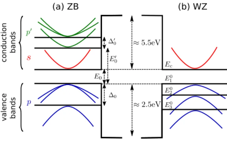
II we present DFT results of the electronic band structure calculation and specifically the spin-orbit coupling induced spin splitting of the bands for a semifluorinated graphene

We introduced realistic spin-orbit coupling model Hamiltonians and provided quantitative values for their parameters that can be used to study spin relaxation, spin transport,

The effective anisotropic exchange model is useful in precise analysis of the physical realizations of quantum computing schemes based on quantum dot spin qubits, as well as in

(a) Electric field induced splittings at the K point as functions of the electric field: (blue circles) and (green squares) shows the splittings of the high-energy conduction

Our new SO term gives rise to a nonzero ballistic spin-Hall conductivity, which changes sign as a function of the Fermi energy (&#34; F ) and can induce an unusual Zitterbewegung

This effect amounts in spin accumulation as a response to an applied in-plane electric field and is therefore a possible key ingredient towards all-electrical spin control