Counting statistics and dephasing transition in an electronic Mach-Zehnder interferometer
A. Helzel,1L. V. Litvin,1I. P. Levkivskyi,2,3E. V. Sukhorukov,4W. Wegscheider,5and C. Strunk1
1Institut f¨ur experimentelle und angewandte Physik, Universit¨at Regensburg, D-93040 Regensburg, Germany
2Theoretische Physik, ETH Zurich, CH-8093 Zurich, Switzerland
3Bogolyubov Institute for Theoretical Physics, 03680 Kiev, Ukraine
4D´epartement de Physique Th´eorique, Universit´e de Gen`eve, CH-1211 Gen`eve 4, Switzerland
5Laboratorium f¨ur Festk¨orperphysik, HPF E 7, ETH Z¨urich, 8093 Z¨urich, Switzerland (Received 31 December 2014; revised manuscript received 12 May 2015; published 16 June 2015) It was recently suggested that a novel type of phase transition may occur in the visibility of electronic Mach-Zehnder interferometers. Here, we present experimental evidence for the existence of this transition. The transition is induced by strongly non-Gaussian noise that originates from the strong coupling of a quantum point contact to the interferometer. We provide a transparent physical picture of the effect by exploiting a close analogy to the neutrino oscillations of particle physics. In addition, our experiment constitutes a probe of the singularity of the elusive full counting statistics of a quantum point contact.
DOI:10.1103/PhysRevB.91.245419 PACS number(s): 73.23.Ad,73.63.Nm The recent discovery of a lobe-type behavior in the visibility
of Aharonov-Bohm oscillations in electronic Mach-Zehnder interferometers (MZI) has triggered extensive theoretical studies in this field. These interferometers were implemented in the edge channels in the integer quantum Hall effect (QHE), mostly for filling factorff=2 [see Figs.1(a)and1(b)] [1–3].
Many sophisticated theories have been proposed to explain the lobes in the differential visibility of Aharonov-Bohm oscillations as a function of the voltage bias [4–11]. While the central lobe and next side lobe are easy to explain, observation of additional side lobes in a number of experiments is considered to be a puzzling phenomenon. Here, we show that this effect can be explained in a rather simple way, if two interacting edge channels are present. The underlying phenomenon turns out to be very similar to that of neutrino os- cillations in high-energy physics: neutrinos oscillate between different flavor states because they are created in a flavor eigenstate, which is not an eigenstate of the Hamiltonian.
Similarly, when an electron wave packet is partitioned by a beam splitter, it excites a collective charge mode, which is not an eigenstate of our model Hamiltonian [6]. At the second beam splitter of the interferometer, this leads to a secondary interference between the collective modes as a function of the applied voltage bias. This model can explain many of the experimental observations [12–16], most importantly the visibility lobes [17] and the phase rigidity of the visibility [1,2].
Dephasing of the Aharanov-Bohm interference results from random fluctuations of the phase that are averaged out by the detector. In our devices, fluctuations are generated by an additional quantum point contact (QPC-0) in front of the interferometer input, which can be controlled by its transmission probability T0. The noisy input current leads to charge fluctuations in the interferometer. The accumulated charge shifts the edge, which leads to the Aharonov-Bohm phase shift. Hence, the strong Coulomb interaction between the edge channels guarantees a strong coupling of the electrons in the interferometer to the noise. The visibility will thus be suppressed by the charge fluctuations induced by partitioning of electrons at QPC-0. Most interestingly, the lobe pattern was predicted to undergo a sudden change atT0 =12 under
such conditions [18]. This noise-induced transition provides a unique experimental signature of the non-Gaussian character of the noise in the MZI visibility.
Current fluctuations at zero frequency are described by the set of irreducible moments (cumulants)Ij, wherej = 1,2, . . ., of the currents’ distribution. Alternatively, the proba- bility distribution can be described by the generatorh(λ)=
jIj(iλ)j/j! of its full counting statistics (FCS) [19].
For Gaussian noise, the FCS generator contains only the first two terms h(λ)= Iiλ− I2λ2/2, where I is the average current andI2is the zero-frequency noise power.
The third cumulantI3vanishes at equilibrium, and thus it provides a measure of the deviations from Gaussian statistics in nonequilibrium state [20–26].
In noise detection schemes in mesoscopic physics the variableλplays the role of a coupling constant, connecting the noise source and the detector [19,27]. The coupling constant is typically very small, which demands long-time measurements. In this case, the high-order cumulants are suppressed because many random events contribute to the detector output signal, and by virtue of the central limit theorem the noise becomes effectively Gaussian. Signatures of non-Gaussian noise have presumably been observed via its effect on the visibility of Aharonov-Bohm oscillations in MZIs [28]. Introducing noise into the copropagating inner edge channel, which was electrically disconnected from the interfering outer edge channel, was shown to reduce the visibility. A particular V-shaped dependence of the visibility νof the interference on the transmission of the copropagating channel was observed and attributed to the non-Gaussian character of the noise. However, that observation could not be reproduced in a similar experiment [29], nor was it linked to the peculiar multiple lobe structure [13,16,17] inν(Vdc) of such interferometers.
Here, we present experimental evidence for a noise-induced nonequilibrium phase transition that was predicted to occur atT0= 12 [18]. This peculiar type of nonequilibrium phase transition is caused by a singularity in the FCS generatorh(λ) of the QPC occurring at λ=π, which leads to a singular dephasing rate of the interferometer under nonequilibrium
d
(e) (f)
(g)
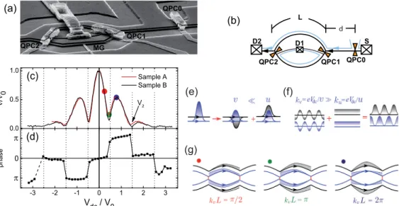
FIG. 1. (Color online) (a) Schematic of the edge channels in the MZI connected to source and drain. The black line is the outer edge channel carrying interfering electrons and the light blue line represents the inner edge channel. (b) Scanning electron micrograph of the sample with marked gates QPC-0, QPC-1, QPC-2 and the modulation gate MG. The black line represents the edge channel used for the interference.
QPC-1 and -2 are set to half transmission and QPC-0 is set to transmit the outer edge with probabilityT0. Ramping the modulation gate alters the area between the electron paths and thus the Aharonov-Bohm phase. (c) Multiple lobe structure: If a dc voltage is applied to the interfering edge channel [black line in panels (a) and (b)] the differential visibility shows a multiple lobe structure with several nodes, which is displayed for two samples A (red line) and B (black line). When the visibility is scaled with respect to the zero-bias maximum visibilityν0and the voltage with respect to the node spacingV0, the curves of the two samples collapse. (d) Phase evolution: The lobes appear as phase-rigid plateaus within the lobes and phase jumps ofπat the nodes. (e) Representation of an electron in terms of charge and dipole plasmon wave packets: In the presence of strong Coulomb interactions, the edge eigenmodes are the fast charged plasmons and the slow dipole plasmons with the linear spectrum in the low-energy limit. (f) Superposition of delocalized charge and dipole modes: An electron injected at the energyeVdcexcites dipole plasmons with wavelengthkv=eVdc/vand charged plasmons with wavelengthku=eVdc/u, so thatkukv. Such superposition of plasmons has alternating zeros and maxima along the edge. (g) Secondary interference of collective modes: At particular values of the voltage bias applied to the interferometer, the plasmon amplitude has a maximum or a minimum at the position of the second QPC, corresponding to constructive or destructive secondary interference.
conditions. This effect can be linked to the perfect entangle- ment between the MZI and the QPC [27], as a consequence of the strong coupling between the two, and may be seen as a manifestation of the quantum origin of shot noise (for details, see AppendixD).
We start by addressing the physics of multiple side lobes in the visibility of AB oscillations in MZIs. This phenomenon was observed experimentally in the visibility functionν(Vdc)=(Gmax−Gmin)/(Gmax+Gmin), whereGis the differential conductance of the interferometer, for a noise- less incident beam and filling factors 2>ff>1.5 [13,16,17].
Figure1 shows an electron micrograph (a) and a schematic (b) of a typical sample, the visibility ν normalized to its valueν0atVdc=0 (c), and the corresponding phase evolution (d). To explain these side lobes, several theories have been proposed [4–11]. Most of the experimental observations can be consistently explained by modeling the QHE edge states as chiral quantum wires supporting copropagating magne- toplasmon modes at ff=2 (for details, see Appendix D).
Coulomb interaction between these modes results in a pair of charged and neutral (dipolar) plasmon modes propagating at different velocities along the edge [see Fig.1(e)]. Because of this velocity difference, charge oscillations introduced in one of the edges can be transferred from one edge to the other, resulting in a collapse of the interference pattern at certain equidistant voltagesVk=(k−1/2)V0, where the node
spacingV0 is inverse proportional to the arms lengthL [6].
This effect is remarkably similar to neutrino oscillations [30], a phenomenon in high-energy physics that manifests itself in the periodic change of the flavor quantum number of freely propagating neutrinos [31].
Next, we sketch the main idea of the theory in Ref. [6], while further details are presented in AppendixD. The many- body wave function of the two interacting edge channels in one of the arms of the interferometer can be decomposed in two components: the charge part |N, where N is total number of electrons in one edge of the interferometer, and the plasmon part|plasmons. An electron tunneling at the first beam splitter (QPC-1) changes the number N by one and excites plasmons:|N → |ψN+1 = |N+1|plasmons. Two components evolve to the final state |ψN+1 at the second beam splitter (QPC-2) and acquire the specific phase shifts.
Combining the two components of the wave functions|ψN+1 and |ψN+1 results in a total probability amplitude for the detection of charge in one of the contacts, say D2:
ψN+1|ψN+1 =e−iπ M1+ei2π M
2 =cos (π M), (1) where the dimensionless parameter
M = eVdcL
2πv (2)
can be interpreted as the average number ofexcesselectrons injected by the source into the outer edge channel during the timeτ =L/vtaken by the slow dipole mode to reach the QPC- 2 (propagating at the speedv). The first factor in Eq. (1) is the phase shift resulting from the voltage-induced accumulation ofM/2 electrons in the outer edge channel, while the second comes from the interference of charge and dipolar plasmons.
The results (1) and (2) indicate that the lobe pattern ob- served in Fig.1(c)originates from the secondary interference controlled byM. The phase rigidity follows from the fact that the overlap is a real function. The only free parameter in the theory of Ref. [6] is the velocityv of dipole plasmons. It is reflected in a characteristic energy
εL=eV0=2πv/L (3) that depends onLonly [32]. For two interferometers of differ- ent arm length,εLis extracted from the position of the second visibility node at voltageV2in Fig.1(c), which corresponds to a value ofV0L=2.8×10⁻¹⁰Vm, orv=1.1×10⁵m/s. For sample A (B), we obtainεL=45.8 (30.6)μeV. In Fig.1(c), a strong damping of the oscillations is seen that has been phenomenologically accounted for by an additional factor D(Vdc)=exp[−(eVdc)2/2ε02] in Ref. [13] with a characteristic energyε0 that is of the same order of magnitude asεL. The damping is an effect of inelastic scattering [33], which is not contained in the theory. In the following, the damping factor will be removed by normalizing the visibilityν(Vdc,T0) with respect toν(Vdc,T0=1).
Next, we give an elementary argument of how the MZI visibility is connected to the FCS generator h(λ) of the quantum point contact QPC-0 with the transparencyT0at the MZI input (see Fig. 1). It is well known [19] that the FCS generator in the long time limit is given by
h(λ)=eVdc
2πln[1+T0(eiλ−1)]. (4) Note that this function displays for λ= ±π a singularity at transmission T0 =12, which in the context of quantum measurements reflects perfect entanglement between the sys- tem (MZI) and the detector (QPC) as a consequence of the strong coupling between the two [27]. The essential point of Ref. [18] is that the overlap of interfering quantum states [Eq. (1)] depends on the number m of excess electrons in the interferometer, injected during the time intervalτ =L/v.
If the transparency of QPC-0T0=1 we have m=M [see Eq. (2)]. Upon reducing T0 below one,m < M becomes a random variable, which fluctuates according to the binomial statistics between 0 andMwith the average valuem =T0M.
For largeM1, we can approximatemto be integer. To find the visibility of the interference patternν one needs to average the overlapψN+1|ψN+1 over the possible particle numbers:
ν(M)=
M
m=0
P(M,m) cos(π m)
, (5)
where P(M,m)=BMmT0m(1−T0)M−m is the the binomial distribution of electron transmissions at the QPC-0, and BMm are the binomial coefficients. The visibility (5) is thus connected to the FCS generator (4) via the Fourier transform
M
m=0P(M,m)eiλm=exp[τ h(λ)]. By setting λ=π, one obtains
ν(M)= |cos[M(2T0−1)]|exp[M ln|2T0−1|], (6) whereis the Heaviside step function, and the nonanalytic structure ofνstems from the singularity inh(λ) atλ=π and T0=12. This is the origin of the noise-induced phase transition predicted in Ref. [18].
The result in Eq. (6) contains an oscillatory and a dephasing factor, which both depend on M and T0. Note that this equation is only valid forM1 and a more rigorous analysis is necessary to find the exact expression (see Appendix D and Ref. [18]). In particular, such analysis shows that first lobe is always present, and its position weakly depends on T0 [34]. For T0> 12, multiple side lobes are expected, with visibility nodes that remain independent ofVdc. For T0<1, the normalized visibility is exponentially damped at large Vdc. From the logarithm in the dephasing term in Eq. (6) one expects a divergence of the dephasing rate at T0=12. The more rigorous treatment in Ref. [18] and our numerical calculations (see AppendixesDandE) take into account the quantum fluctuations ofmand result in a divergence of the spacing between visibility nodes, whenT0approaches12.
In the following, we show that all of these rich and intriguing predictions are observable in our experiment, and provide clear evidence for the non-Gaussian character of the noise. In Fig.2, we present the evolution of the lobe pattern when we introduce noise to the interfering edge channel of
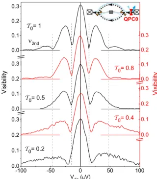
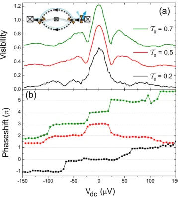
FIG. 2. (Color online) Visibility lobe structure of sample B (L= 8.7μm) for differentT0: When closing QPC-0 (see inset) belowT0= 1 the node positions remain essentially unchanged for transmissions T00.5, i.e., multiple side lobes with the same widths of lobes and position of nodes as forT0=1. The lobe height is strongly reduced at finite dc bias. BelowT0= 12, the lobe structure changes from the multiple side lobe behavior to a single side lobe behavior. The central lobe width increases with decreasing transmission and the first side lobes are stretched to large bias.
-150 -100 -50 0 50 100 150 T0 1.0
0.5
Phase derivative (a.u.)
Vdc (μV)
0.2
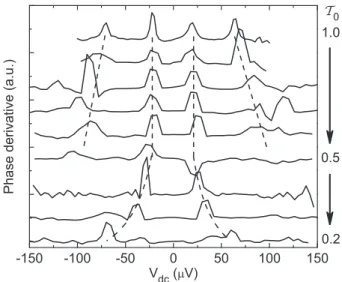
FIG. 3. Phase changes of sample A (L=6.5μm) for different T0: similar to Fig.1(d)the steps in the phase evolution at visibility nodes become discernible as peaks in the numerical derivative dϕ(Vdc)/dVdcof the phase for different transmission of QPC-0 (from 1.0 to 0.2 in steps of 0.1). The width of the inner pair of phase steps remains nearly fixed forT0>0.5. Upon a further decrease ofT0, the width of the central lobe is increasing.
the MZI by closing QPC-0 (see the inset in Fig.2) so that the outer edge channel is only partially transmitted. ForT00.5, the number and position of the visibility nodes stays (almost) constant, while the height of the second side lobe is gradually suppressed. The number of the side lobes and the phase rigidity is more clearly seen in the derivativedϕ(Vdc)/dVdcof the phase plotted in Fig.3. Close toT00.5, a second node is hard to see in Fig.2, but a drop to zero visibility and the phase jump is still apparent in the gate modulation of the MZI current in Fig.3.
Some structure is also seen at T0=0.5 (see Appendix C), namely, the phase jumps shown in Fig.11.
The situation changes drastically forT0 0.5 when multi- ple nodes and multiple side lobes disappear abruptly. This is seen very clearly in Fig.3. The central lobe width is increasing with decreasing QPC-0 transmission, i.e., the remaining single phase step shifts to high voltages and no additional nodes can be seen (see Fig.2).
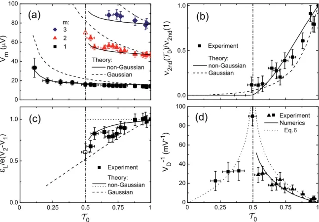
Next, we present a detailed and quantitative comparison of the dependence of the measured position of the visibility nodes and the height of the second side lobe onT0 with numerical calculations (see AppendixE) that extend the predictions of Ref. [18]. In Fig.4(a), we plot the positionsVm of the first three visibility nodes versusT0for sample B. ForT0=1, these are expected atVk =(k−1/2)εL/e. Only the first visibility node is observed in the whole range of transparencies 0.1 T01. The presence of the second and third visibility nodes is limited to the range 0.5T01, as predicted for non- Gaussian noise only. For decreasing transparencyT0, the nodes shift outward in a way that is captured quantitatively by our numerical calculations (full lines) when using the value for the velocity of dipolar plasmons determined from Fig. 1(c).
The dashed lines arise, when Gaussian noise is modeled by truncating the Taylor expansion of the FCS generator [Eq. (4)]
inλafter the quadratic term. In this case, a stronger variation of
all visibility nodes withT0is expected, and the second and third nodes should exist also belowT0 =0.5. The observed absence of visibility nodes withk >1 is thus a strong evidence for the non-Gaussian character of the noise. The position of the first visibility node is slightly reduced with respect to the expected valueεL/2e.
According to our theory, the amplitude of the second side lobeν2nd(T0) vanishes in a universal quasilinear fashion near T0=0.5, i.e., it is independent of the system parameters v andL. In Fig.4(b), we present the ratioν2nd(T0)/ν2nd(T0=1) of the maximal visibility amplitudesν2nd(T0) determined from sweeps of the modulation gate. The normalization with respect to ν2nd(T0=1) is necessary, to divide out the additional dephasing factorD(Vdc) discussed above. Within the limits of the experimental accuracy, our data are again in good agreement with the theory.
In order to illustrate the character of the transition, and demonstrate the agreement of the measured data with the structure of Eq. (6), we illustrate the peculiar variation of the arguments of the cosine and exponential factors in Eq. (6) versusT0. Figure4(c)shows the variation of the inverse node spacingεL/[e(V2−V1)] extracted from Fig.4(a). Instead of a step function (dotted line) expected from the elementary argument leading to Eq. (6), a rounding of the step is found that results from quantum fluctuations ofn and agrees well with our numerical calculation (full line). On the other hand, the Gaussian truncation of the FCS predicts a linear decay from 1 to 0 (dashed line) rather than a step. Again, the absence of higher visibility nodes below T0= 12 demonstrates the essential contribution of the higher cumulants contained in Eq. (4). Moreover, the abrupt decay ofεL/[e(V2−V1)] at the transition pointT0= 12 suggests to consider this quantity as a normalized order parameter for the nonequilibrium phase transition predicted in Ref. [18].
In Fig.4(d), we display the peaked behavior of the dephas- ing rateVD−1(T0)=(e/2L) ln|2T0−1|defined by Eq. (6). The points were extracted from Fig.4(b) for T0>0.5, and the exponential tails ofν(Vdc) in Fig.2forT00.5. We see that VD−1(T0) shows indeed a pronounced peak at the transition pointT0=0.5 which decays in a way that is quantitatively reproduced by the theory, using again the same value for the velocity of dipolar plasmons determined from Fig.1(c).
The singular dephasing rate at the transition point reflects the dominance of the non-Gaussian noise at the nonequilibrium phase transition.
We have seen that our model, despite being simple, is able to explain quite sophisticated phenomena such as the lobes in the visibility of AB oscillations and the non-Gaussian noise- induced phase transition. Therefore, it seems that our model is able to grasp the essential physics of dephasing in MZIs.
However, it remains to discuss to what extent the predictive power of our theory is robust against various modifications of the model. In this connection, we wish to mention the recent paper [11], which investigates AB oscillations in the MZI at integer filling factors using a model with a different form of the interaction potential. Namely, in contrast to our model, where the interaction extends outside the interferometer and is approximated by a short-range potential, the authors of Ref. [11] consider an opposite extreme where the interaction is
6
FIG. 4. (Color online) Nodes, lobes, and the phase transition: (a) Dots: measured visibility node positionsVm vs the transparency of QPC-0. The nodes shift outward, and disappear form >1 atT0= 12. Solid lines: predictions of the full theory using the characteristic energy εL=30.6μeV extracted from Fig.1(c). Dashed lines: Gaussian approximation of the theory. (b) Dots: maximal visibility (ν2nd) of the second side lobes [see Fig.2(sample B)], normalized with respect toν2nd(T0=1). Solid (dashed) line: theoretical prediction for the full theory (its Gaussian approximation). While the Gaussian approximation predicted multiple side lobes for all values ofT0, they appear in the full theory only forT0larger than 0.5. (c) Inverse normalized node spacinge(V2−V1)/εLas a signature of the nonequilibrium phase transition. Full line:
full numerical calculation of the node spacing. Dotted line: expectation from the approximation of Eq. (2). Dashed line: Gaussian approximation of the full theory. The dashed-dotted line indicates the point of the phase transition. In the presence of non-Gaussian noise the inverse node spacing vanished abruptly at the transition pointT0= 12. (d) Dephasing rateVD−1extracted from the exponential decay ofν(Vdc) in Fig.2for T0 12 (squares) and the amplitude of theν2nd(Vdc) in (b) forT0> 12(triangles). The dotted line represents the dephasing rate extracted from Eq. (6), while the solid line is the result of the numerical simulations. No free parameters are adjusted in the theory curves of all four panels.
localized inside the MZI between two QPCs, and the potential is approximated by a “capacitance model,” i.e., it is maximally long range.
Concerning the lobe structure, the results of Ref. [11] for ff=2 and for strong interaction limit fully agree with our findings as well as with the results of the earlier paper [6], where our present model has been thoroughly analyzed. We note that the authors also predict lobes for the case offf=1.
However, their moderate interaction limit, where the lobes are predicted, is not quite consistent because the long-range Coulomb interaction is effectively always strong. Moreover, Ref. [11] neither makes any attempt to interpret the physical origin of predicted lobes, nor it discusses to what extent they are robust against the variation of the transparencies of the QPCs of the MZI. In any case, the predicted behavior atff=1 seems to have no relation to the phenomenon investigated in this paper.
In conclusion, our work constitutes a detailed investigation of the effect of non-Gaussian noise on the visibility of interference in electronic interferometers. The lobe and node structure of the visibility directly reflects the peculiar analytic
structure of the generator of the full counting statistics of a quantum point contact. It provides experimental evidence of a singularity in the FCS that is intrinsic to binomial statistics, and that induces a peculiar type of nonequilibrium phase transition. In addition, the excellent overall agreement of the observed behavior of the visibility with the predictions of the plasmonic edge model provides firm evidence that the latter captures the essential physics behind the complex interference phenomena observed in Mach-Zehnder interferometers with two copropagating edge channels.
We want to thank K. Kobayashi, H. S. Sim, and S.
Ludwig for fruitful discussions and H.-P. Tranitz for growing the GaAs/AlGaAs-material. The work was funded by the Deutsche Forschungsgemeinschaft within the SFB631 “Solid state quantum information processing” and by the Swiss National Science Foundation. C.S. and E.V.S. conceived the experiment. L.V.L. and A.H. fabricated the samples, conducted the measurements, and analyzed the data. I.P.L. and E.V.S.
provided the numerical data. All authors contributed to the writing of the manuscript.
QPC0
QPC1 QPC2
(a)
MG
S QPC1 QPC0
QPC2 D2 D1 (b)
d L
V ~ Vbias
FIG. 5. (Color online) SEM picture and sketch of the sample:
(a) Scanning electron micrograph of the sample with marked gates QPC-0, QPC-1, QPC-2 and the modulation gate MG. The black line represents the interfering edge channel with QPC-1 and -2 set to half transmission of the outer edge channel. QPC-0 fully reflects the inner and partially transmits the outer edge channel. (b) Schematic of the relevant edge channels in the MZI in addition to the source S, the drains D1 and D2, and the QPC-1, -2, and -0. The black line is the outer edge channel carrying interfering electrons and the light blue line represents the inner edge channel. QPC-0 is adjusted to reflect the inner edge channel (blue). Important sample dimensions are the length of the interferometer armsLand the distancedbetween QPC-0 and -1.
APPENDIX A: EXPERIMENTAL METHODS The results are obtained on two samples made from differ- ent wafers. Sample A was structured in a modulation-doped GaAs/GaxAl1−xAs heterostructure with a two-dimensional electron gas (2DEG) 90 nm below the surface. The 2DEG density and mobility are n=2.0×10¹⁵ m−2 and μ= 206 m2/(Vs) at 4 K on the unpatterned wafer. Sample B was patterned in another heterostructure also with a depth of the 2DEG of 90 nm, but with n=2.1×10¹⁵m−2 and μ=289 m2/(Vs) at 4 K on the unpatterned wafer. The exact patterning procedure is described in Ref. [3]. The arm’s length Lof the interferometers is estimated to be 6.5μm for sample A and 8.7μm for sample B. The structures contain not only the MZI, i.e., QPC-1 and -2 and two drains, but also an additional quantum point contact (QPC-0) between source and MZI. This QPC-0 is situated a distance D=5μm for sample A and 8μm for sample B in front of QPC-1 (see Fig.5).
A standard lock-in technique (f ∼300 Hz) was used to measure the output current via voltage drop between terminal D2 and another (grounded) Ohmic contact. An ac voltage of 1 μV plus a dc voltage Vdc were applied to measure the differential conductanceG(Vdc)=dI(Vdc)/dVdc. By comparing the temperature dependence of the visibility in Ref. [13] (the bath temperature of the dilution refrigerator was measured with a RuOx thermometer) with that in Ref. [35], where the electron temperature in the interferometers was measured directly via the thermal noise, we estimate the electron temperature in the present experiment to be close to 30 mK. Sample A was measured at a magnetic field of 4.73 T (ff =1.7) and with ideal configuration of the QPCs a (maximum) visibility of 65% atVdc=0 is achieved, sample B at 4.5 T (ff =1.8) with a maximum visibility of 33.5%.
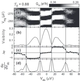
0 0.1 0.2 0.3 -260 -270
Vmg(μV)Visibility
T0 = 0.88
0
-π
Δϕ
π
-80 -60 -40 -20 0 20 40 60 80
(d) (c) (b)
dϕ dVdc
Vdc (μV ) (a)
0.36 0.39
GD2 (e2/h)
FIG. 6. Raw and processed data: (a) grayscale plot of the measured conductance G(Vdc,Vmg) for T0=0.88. Checker-board pattern of dark and bright regions reveals central lobe and two additional lobes on each side. (b) The visibility of the oscillatory conductance in (a), extracted according to Eq. (A1). (c) The AB-phase shiftϕwith respect toVdc=0 obtained from fits of tracesG(Vmg) with Eq. (A2). Constant phase inside lobes and jumps ofπat nodes can be seen. (d) The numerical derivative ofϕfurther highlights the position of the nodes as pronounced peaks.
Analysis
We measured dI /dVdc=G versus Vdc for a range of modulation gate voltageVMG. An example of raw data can be seen in Fig.6(a). The sinusoidal oscillations for rampingVMG and the decaying oscillations forVdcare well defined. In the raw data, the multiple side lobes can be seen as a chessboard pattern that fades out at largerVdc. We extract the differential visibility
ν(Vdc)=Gmax(Vdc)−Gmin(Vdc)
Gmax(Vdc)+Gmin(Vdc) (A1) of the interference pattern at each bias voltageVdc[Fig.6(b)].
The Aharonov-Bohm phase and the visibility in Fig.2of the main part are determined from sine fits of modulation gate traces at certainVdcrelative to the trace at zero bias [Fig.6(c)].
We fit the measured modulation gate traces to
G(Vmg) = Gav+Goscsin(Vmg/Vp+ϕ) (A2) with the four parameters Gav, Gosc, Vp, and ϕ=ϕ(0)− ϕ(Vdc). For a measurement of each transmission T0 we fit the period Vp only once for the large oscillations at zero bias and then keep it fixed for the other traces of one measurement. Examples of typical modulation gate traces and the corresponding fit curves can be seen in Fig. 7 for transmissions 0.57 and 0.54. In this way, we trace the phase evolution at the frequency of interest even if it is nearly buried in noise. This becomes crucial for very small oscillation amplitudes. From such fits we determinedν2ndin Fig.4(b)of the main part for transmissionsT0close to 0.5.
FIG. 7. (Color online) Sine fits of gate traces: On the left the visibilities vs Vdc for TQPC−0=0.57 (top) and 0.54 (bottom) are displayed. On the right are according modulation gate traces (black line) of the markedVdc(dashed vertical lines in the left plots) at the center of the lobes and their sine fits (red line). ForVdc≈75μV, only residual oscillations buried in noise are present.
Figure 6(d) shows the numerical derivative of ϕ(Vdc) to highlight the phase jumps at the nodes, as it is used in Fig.3, main part. For the evaluation of the node positionsVmand the height of the second side lobe in Fig.4of the main part, both visibility and phase evolution are analyzed to determine the node positions.
APPENDIX B: CHARACTERIZATION OF THE INTERFEROMETERS
Two samples are studied, which differ in interferometer arm length L and distance d (see Methods). The maximal two-terminal conductance is≈2e2/ h, corresponding to two transmitted edge channels. We use QPC-0 to selectively bias the outer edge channel, while the source terminal of the inner channel is left grounded (T0=1). QPC-1 and -2 are set to reflect the inner channel, implying that the interference takes place only in the outer edge channel. At zero bias we reach maximal interference visibilities (ν0) of 65% in sample A and 33.5% in sample B. Aside from the maximum visibility ν0 the lobe periodicity V0 is different for the samples. Both parameters depend on the magnetic field, the temperature, and the arm lengthLof the interferometer [13,18,36].
The visibilityν0at zero dc bias decreases exponentially with L, ν∝exp(−2L/ lϕ), with the coherence length lϕ∝T−1, similar to the data in Refs. [13,36]. The different maximum visibilities of the two samples result from the different sizes L, affecting bothν0andV0. The normalized visibility pattern ν(Vdc/V0)/ν0 in Fig. 1(c) of the main part turns out to be independent of L. We can conclude that for T0=1 the differences between both samples are controlled by only one parameter, i.e., the L-dependent characteristic energy εL=2πv/L. The presence of visibility nodes is even more apparent in the evolution of the Aharonov-Bohm phase. In the visibility only two side lobes can be seen clearly, whereas the analysis of the residual oscillations at high-bias voltages by
dc
T0
T0
T0
(a)
(b)
FIG. 8. (Color online) Evolution of the lobe structure in sample A: visibility (a) and phase shift (b) vs dc bias voltage for various transmissions of QPC-0 for sample A. ForT00.5, multiple side lobes are present in the visibility and the phase evolution, similar to sample B. ForT0=0.2, we see a wide central lobe and only single side lobes. The position of the nodes is clearly visible in the phase behavior by jumps and we can deduce the lobe structure.
sinusoidal fitting (see methods) display one more phase jump, revealing a third side lobe in sample B.
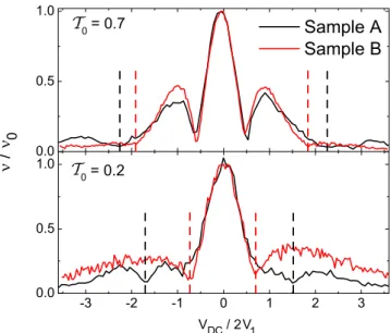
APPENDIX C: COMPARISON OF SAMPLES A AND B In the main part, we mainly display data obtained on sample B. Here, we present an overview of the lobe structure for sample A in Fig. 8. The qualitative behavior in sample A is similar to sample B, i.e., the positionsVm of the multiple side nodes [see Fig.8(a)] and the phase jumps [see Fig.8(b)]
remain fixed forT0>0.5 and the locationV1of the single side node increases forT0<0.5. Such behavior is also seen in the numerical derivative ofϕ(Vdc) (Fig.3 of the main part). For T0=1, we can match the visibility curves for the two samples very well by normalization with respect to the node spacingV0 and the zero-bias visibilityν0[see Fig.1(c)in the main part].
In contrast, for lower transmissions T0<1 of QPC-0, differences between samples A and B remain, which originate from the operation of QPC-0 as a source of current noise at the interferometer input. In Fig. 9, the discrepancies are shown for two exemplary transmissions T0=0.7 and 0.2.
The voltages are scaled with respect to 2V1 extracted from the trace withT0 =1. The measurement of the phase shift in Fig.8(b)allows an unambiguous determination of the node positionsVm, which are marked by the dashed lines in Fig.9.
Because of the scaling the first visibility nodes match, but the second visibility nodes disagree forT0=0.7. Moreover, even
T0
T0
2 1
FIG. 9. (Color online) Differences between samples A and B: the visibility forT0=0.7 and 0.2 of both samples are shown. The dashed lines mark the position of the second nodes (upper panel) and first nodes (lower panel) for samples A (black) and B (red). Although for T0=1 the curves for samples A and B coincide after scaling byν0
andV0, this is different for lower transmission of QPC-0.
the first visibility nodes of the two samples do not collapse for T0=0.2. In addition, a foot develops inνnearVdcV1.
The overall variation ofV1 versusT0 for both samples is shown in Fig.10together with theory curves for the Gaussian and non-Gaussian cases. For lower transmissions, the shift of V1 with transmission is much stronger for sample A, when compared with sample B.
BelowT0 =0.5, a crossover from non-Gaussian to Gaus- sian behavior is observed for sample A. This observation can be made plausible by the following argument: at finite
T 11
T
FIG. 10. Evolution ofV1(T0): The position of the first nodeV1
follows the non-Gaussian prediction for largeT0. For transmissions T0<0.5 the voltage V1 of the first visibility node (dots) grows more rapidly for sample A than for sample B, indicating a crossover from non-Gaussian (solid line) to Gaussian (dashed line) behavior, in particular for sample A.
voltages the statistics of the particle numbers transmitted through QPC-0 is expected to be non-Gaussian [19]. It was shown in Ref. [37], however, that a weak nonlinearity in the spectrum of the plasmon modesk(ω)=ω/v+γ ω2sign(ω) can suppress the contributions of higher-order cumulants in the FCS generator for distancesLg =1/(γ T Vdc)2 that strongly depend on the bias voltage Vdc. Such a nonlinear plasmon dispersion relation can also lead to a nonlinear conductance of the QPC. A crossover to Gaussian noise can result from a decrease ofLg(Vdc) with largerVdc, or from sufficiently strong nonlinearity of the plasmon dispersion relation in sample A, which ensureLg < d already at small voltages. We checked carefully that sample B shows negligible nonlinearities in the current-voltage characteristic of the QPCs. This is consistent with the observed non-Gaussian behavior of the visibility.
On the other hand, we found that sample A has strong nonlinearities in the conductance. Because the arm lengthLof interferometer A is smaller, the important energyεLand thus the required voltagesVmare larger in sample A (the ratioL/d is similar in both samples). Together with the strong voltage dependence of Lg this may explain the observed crossover from non-Gaussian to Gaussian behavior ofV1 forT0<0.5 andV2forT0>0.5 in Figs.9and10. The larger characteristic energyεLof sample A makes it more prone to a suppression of higher-order cumulants at larger voltages, when compared with sample B.
From Ref. [18] it is expected that there are no multiple side lobes atT0=0.5. In contrast to this prediction, we observe traces of a second side lobe in our experimental data atT0 = 0.5, in particular, for sample A (see Figs.8and 2, main part).
Figure11shows the measured phase shifts for both samples at this point. After the jump of the phase from 0 toπ at the visibility node a further gradual shift of the phase towards higher values can be clearly seen. The additional phase shift saturates at π/2 for sample A. In sample B, only residual
dc 2 T0 = 0.5
FIG. 11. (Color online) AB-phase evolution at the phase transi- tion: forT0=0.5 (measured forVdc=0) multiple side lobes are observed for sample A. In sample B, only single side lobes are visible with a width similar toT0>0.5. The phase evolution shows in both samples a jump ofπ at the first node. In sample A, we clearly see a further increase of the phase that saturates near 3π/2. The second side lobes are pronounced. Sample B shows a similar unexpected behavior.
traces of an additional side lobe are visible, which also do not obey phase rigidity. The fact that multiple side lobes are observed nearT0=0.5 may be explained by a variation ofT0
withVdc that are consistent with the observed nonlinearities of the QPCs of sample A [38], and result in a transmissionT0
at finiteVdc, which slightly increases withVdc. On the other hand, the deviations from phase rigidity observed in Fig.11 cannot be understood in this way.
APPENDIX D: THEORETICAL METHOD
In the main part of the paper, we present an explanation of the lobe-type pattern of visibility in electronic MZI in simple physical terms. A more rigorous description of QH interferometers at filling factor 2, proposed in Ref. [6], is based on the so-called bosonization approach. Here, we summarize this approach in order to support the elementary derivation given in the main part of the paper. For simplicity, we set e==1 in the beginning and restore physical units at the end of calculations.
Our experiment addresses the physics of MZIs at low energies compared to the Fermi energy and at long distances compared to the magnetic length. The low-energy spectrum of excitations of chiral edge states consists of the collective charge density oscillation (plasmons). Using second quanti- zation language, these excitations are described by creation and annihilation operators, satisfying the bosonic commutation relations
[asαk† ,asβk]=δssδαβδkk, (D1) where s=1,2 enumerates two arms of the interferometer, α=1,2 enumerates two Landau levels at filling factor 2, and k is the wave vector. Namely, 1D charge densities may be expressed as
ρsα(x)=(1/2π)∂xφsα(x) (D2) in terms of boson fields
φsα(x)=ϕsα+2π Nsαx/W +
k>0
2π/kW(eikxasαk+e−ikxasαk† ), (D3)
which satisfy the canonical commutation relations [∂φsα(x),φsβ(y)]=2π iδssδαβδ(x−y). Here, W is the total size of the system (to be taken to infinity in the end of calculations), and the operatorsϕsαandNsαare the so-called zero modes, i.e, the modes with k=0: Nsα=
dx ρsα(x) is the total number of electrons in the channel (s,α), and operators exp[−iϕsα] increase this number by 1.
The key idea of the bosonization technique is to express the electron creation operators in terms of the boson fields:
ψsα†(x)=exp[−iφsα(x)]. (D4) With the help of Eqs. (D1)–(D3), one can check that (i) so- defined operators obeyfermionic anticommutation relations;
(ii) they create local excitations with unit charge, i.e., they commute with charge density operators as [ρsα(x),ψsα† (y)]= δ(x−y)ψsα†(x). When acting on the state of the interferometer, such operator first increases the total number of electronsNsα
by one, and second, it creates a bunch of plasmon excitations localized near the pointx, as can be easily seen from Eq. (D3).
The convenience of the bosonization approach is in the fact that the Hamiltonian of interacting 1D electrons is quadratic in terms of the boson fields and can be easily diagonalized. In particular, it has been shown in Ref. [6] that the Hamiltonian of electrons interacting via the short-range potentialU(x,y)= U δ(x−y) can be written as
H= 1 2
s,α,β
W
0
dx Vαβρsα(x)ρsβ(x), (D5) where the inverse “capacitance” matrixVαβ=U+2π vFδαβ
contains the Fermi sea contribution with the Fermi velocity vF. It is easy to see that this Hamiltonian can be rewritten in the diagonal form
H=
W
0
dx
4π[u[∂xφ˜s1(x)]2+v[∂xφ˜s2(x)]2] (D6) in terms of the charge and dipole modes φ˜s1,2(x)= [φs1(x)±φs2(x)]/√
2. Note that the velocity of the charge modeu=U/π+vFis much larger then the velocity of dipole modev=vF in the limit of the strong interactionU vF, which applies, e.g., for Coulomb interactions screened at relatively long distances. The new plasmon operators
˜
as1k= 1
√2(as1k+as2k), a˜s2k= 1
√2(as1k−as2k) (D7) have a simple physical meaning: they create and annihilate charge and dipole plasmon excitations with the wave vectork.
Next, we note that the zero-mode contribution VαβNsαNsβ/2Wto the Hamiltonian (D5) can be interpreted as an energy of a capacitor with capacitance matrixW Vαβ−1. Using this fact, one can find the average value of the charge operators in terms of electrochemical potentials μα. In particular, the total number of electrons in the upper outer channel reads as NU1=W
V1α−1μαW μ1/4π v, for μ2=0, and where we have neglected small contribution
∼1/u. Thus, according to Eqs. (D3) and (D4), the excitations created by electron tunneling acquire the following phase from zero modes (restoring physical units and settingμ1 =eVdc):
δϕ0= −W μ1/4πv·2π L/W = −eVdcL/2v, (D8) which explains Eq. (5) in the main text.
Let us now consider the dynamical phase acquired by the plasmons. From the Hamiltonian (D6), it follows that
˜
as1k(t)=e−iukta˜s1k, a˜s2k(t)=e−ivkta˜s2k. (D9) These relations determine the time evolution of the electron operator (D4). On the other hand, the wave-function overlap introduced in the main part of the paper may be written as
ψN+1|ψN+1 ∝
dt eμ1tN|ψU1(0,0)ψU†1(L,t)|N, (D10) where the time integral projects an electron onto the energy μ1, with which it is injected. The similar contribution from the lower arm of the interferometer has been omitted for the sake of simplicity of the argument.
The complication in the next step arises because each electron operator on the right-hand side of (D10) generates an infinite number of terms, when expanded in the plasmon operators, which can be schematically expressed as fol- lowing: ψN+1|ψN+1 ∝
{k,k}C{k}C{k}e−i(K+K)Lδ(μ1+ Ku+Kv), where C{k} and C{k} are the plasmon cor- relation functions for the sets of wave numbers ki and ki, and K=
iki, K=
iki. Here, we have used Eqs. (D3), (D4), and (D9) and integrated over time t to obtain the energy-conserving delta function. It is easy to see that in the large-L limit, the summation over all pos- sible plasmon excitations leads to fast oscillations in the above expression and to the suppression of corresponding contributions. However, two terms in this sum, the sepa- rate contributions of the dipole and charge mode, consti- tute an exception: ψN+1|ψN+1 ∝
{k}C{k}e−iKLδ(μ1+ Ku)+
{k}C{k}e−iKLδ(μ1+Kv). Thus, as a conse- quence of the linear spectrum of plasmons (and of the chirality of the system), we immediately arrive at the expression ψN+1|ψN+1 ∝eiμ1L/u+eiμ1L/v, which justifies our sim- plified approach in the main part of the paper, leading to Eq. (4). In the limituv, restoring physical units and setting μ1=eVdc, the relative phase shift due to the dipole mode reads as
δϕd=eVdcL/v. (D11) Note that the universality of the ratioδϕd/δϕ0= −2, which follows from strong interactions at QH edge, explains the origin of the phase rigidity and phase transition phenomena observed in our experiment.
APPENDIX E: NUMERICAL RESULTS FOR GAUSSIAN AND NON-GAUSSIAN NOISE VERSUS
EXPERIMENTAL DATA
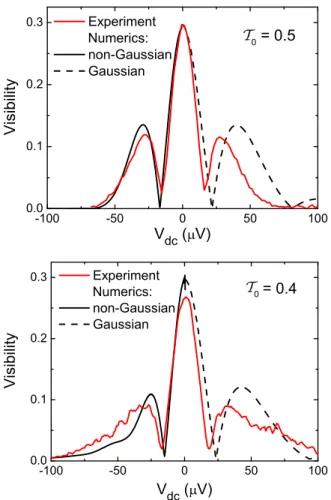
In the main part of this work, we illustrated the qualitative signatures of the phase transition when going fromT0>0.5 to T0<0.5. Here, we want to go more into detail of the expected differences in the visibility characteristics predicted for Gaussian and non-Gaussian noise. In Fig.12, we compare two traces ofν(Vdc) forT0=0.5 and 0.4 with the results of the numerical calculations described in the following.
Reference [18] provides analytically derived large-bias asymptotics of the visibility of AB oscillations in Gaussian and non-Gaussian regimes. These asymptotics are based on the Levitov-Lesovik formula [19] for the long-time behavior of the FCS generator of tunneling currents at the QPC-0.
However, large-bias asymptotics are not sufficient for a direct comparison with our experimental results. For this reason, we follow the approach proposed in Ref. [18] and evaluate the FCS generator numerically. To this end, we use the determinant representation of the FCS generator (see Refs. [19,39]) which allows one to express this generator as a determinant of a single-particle operator:
eiλN(t)e−iλN(0) =det{1−f(ε)+exp[iλU(t)⊗S(ε)]f(ε)}, (E1)
T0
T0
FIG. 12. (Color online) Comparison to theory forT0=0.5 and 0.4 of sample B. In the fits of Gaussian (right half of graphs) and non-Gaussian (left half of graphs) noise, the only free parameters areν0andV2 atT0=1. The better agreement to the non-Gaussian prediction is obvious.
where f(ε) is the energy distribution function, U(t) is the projector on the time interval [0,t], andS(ε) is the scattering matrix of the QPC-0.
We introduce a finite bandwidth for the electrons in the incoming channels of QPC-0 and fix it to be 4000 times larger than the level spacing. Thus, we reduce the problem of finding the FCS generator to the evaluation of the determinant of a finite matrix of the size 4000× 4000. The evaluation of such a determinant as a function of timet and of the transparency T0 can be trivially parallelized and has been done using the Blue Gene/P machine [40]. Then, we evaluate numerically the integral in the Eq. (3b) of Ref. [18], which connects the visibility and the FCS generator via Eqs. (3a), (3b), (4), and (7) of Ref. [18], and find the visibility as a function of the voltage bias and of the transparency.
To compare these numerical data to the experiment we determineν0, from the data of T0=1, and the position of the second nodeV2 atT0=1 as in Fig. 4in the main part.
Figure12shows the bias-dependent visibility forT0=0.5 and 0.4 in sample B with the numerical calculation for Gaussian and non-Gaussian noise. As one can see the nodes for the Gaussian prediction are expected for larger voltages as in the measurement and an additional side lobe should be present
with a height that should be measurable. The curve for the non-Gaussian prediction fits much better and the only small discrepancy is the height of the side lobe. This observation suggests again a strong, almost diverging, dephasing charac- teristic for the non-Gaussian noise distribution expected after QPC-0. The situation is similar for T0=0.4: multiple side lobes and position of nodes of the Gaussian prediction do not fit the measurement.
In conclusion, the two parameters ν0 and V0 determined independently atT0=1 fix the whole set of visibility curves calculated for Gaussian and non-Gaussian noise at different T0. The experimental data agree much better with the non- Gaussian than with the Gaussian curves for all transmissions T0. This provides striking evidence for the noise-induced phase transition proposed in Ref. [18].
APPENDIX F: QUANTUM MEASUREMENTS, ENTANGLEMENT, DEPHASING, AND
NON-GAUSSIAN NOISE
It is instructive to consider the relation of the phase transition phenomena observed in our experiment to the quantum measurement problem. In this section, we show that the comparison of the MZ interferometer to a quantum two- level system, although not being precise, leads nevertheless to an important conclusion that the origin of the observed phenomenon lies in the perfect entanglement between elec- trons injected through the QPC-0 toward the interferometer and those in the superposition of occupying the upper or the lower arm of the interferometer.
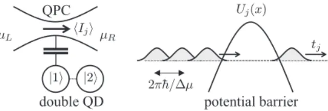
A two-level system, e.g., a double quantum dot (QD) or a spin of electron, which interacts with electrons in a QPC (see Fig.13) is an archetypal example of a quantum measurement setup. This situation is relatively easy to describe theoretically, and nevertheless, it contains essential physics. It also illustrates a dual character of a quantum measurement process. On one hand, one may consider the QPC as a detector of the state of the two-level system. Namely, by applying the electrochemical
FIG. 13. A double quantum dot (QD) capacitively coupled to a QPC as an elementary example of a quantum measurement setup is schematically shown on the left. The QPC connects two electron reservoirs, biased with the electrochemical potential differenceμ= μR−μL. This causes the charge current through the QPC, which takes two average valuesIj,j=1,2, depending on whether the state |1 or |2 of the double QD is occupied. The simplified microscopic picture of the electron transport through the QPC is shown on the right. Electrons at Fermi level, incident from the left reservoir, collide with the potential barrier of the QPC,Uj(x). Because of the capacitive coupling to the double QD, the potential Uj(x) depends on the state|jof the double QD. Therefore, the transmission and reflection coefficientstjandrjand, as a consequence, the average current through the QPCIj, depend on the state of the double QD.
potential differenceμto the QPC, one generates the current, which on the time scale 2π/μ or longer, depending on the character of coupling between two systems, acquires one of the two values I1 or I2, corresponding to the final states of the two-level system. At the same time, in the course of the measurement process, the current noise of the QPC dephases the quantum state of the two-level system, i.e., suppresses the off-diagonal elements of its density matrix.
This leads to the idea [19] to operate the setup in a dual mode, where the two-level system serves as a detector of the noise of the QPC: the off-diagonal elements of the density matrix of the two-level system can be used as a measure of the FCS of the QPC’s current noise.
The advantage of this gedanken experiment is that it can be theoretically described using the single-particle scattering approach. Here, we follow the analysis of Ref. [27], allowing us to account for strong coupling between the QPC and the two-level system. Let us assume that the two-level system is initially in the pure quantum state
jcj|j, j =1,2. The interaction between the QPC and the two-level system affects the QPC’s potential barrierUj(x), which is experienced by the electrons incident at the QPC from the left reservoir (see Fig. 13). The potential barrier reflects an incident electron
|in to the left outgoing state |L with the amplituderj and transmits it to the right outgoing state|Rwith the amplitude tj. As a result, the initial uncorrelated state of the whole system
|in ⊗
jcj|jevolves to the final pure state
|ψ =
j
cj(rj|L +tj|R)⊗ |j. (F1) Taking a partial trace over electronic states|Land|R, one finds that the initial reduced density matrix of the two-level systemρj k(0)=cjc∗kevolves to the following final state:
ρj k(1)=ρj k(0)(tjtk∗+rjrk∗) (F2) after the passage of one electron through the QPC. Applying this stepN times, one finds the reduced density matrix after the passage ofNelectrons:
ρj k(N)=ρj k(0)(tjtk∗+rjrk∗)N. (F3) Thus, if electrons arrive with the rate=μ/2π, the off- diagonal elements evolve as
ρ12(t)=ρ12(0)eht, whereh=ln(t1t2∗+r1r2∗). (F4) It takes time of the order of 1/ to resolve two average current levelsIj =|tj|2from the background of the current noise Ij2 =|tj|2(1− |tj|2) and, thus, to measure the state of the system. This measurement process is intimately related to dephasing: Since|t1t2∗+r1r2∗|1, off-diagonal elements of the density matrix of the two-level system decay with the rate of the order of.
Next, we change the point of view and consider the two- level system as a detector of the current noise created by the QPC. Reference [19] proposes to place the two-level system to the right of the QPC and away from the scattering region, so that the only effect of coupling is to induce the scattering phase shiftλ, so that|t1|2= |t2|2=T. Neglecting the overall phase shift, the functionhin Eq. (F4) acquires the familiar