Tunneling mechanism in a (Ga,Mn)As/GaAs-based spin Esaki diode investigated by bias-dependent shot noise measurements
T. Arakawa ,1,2,*J. Shiogai ,3M. Maeda,1M. Ciorga ,4M. Utz,4D. Schuh,4Y. Niimi ,1,2M. Kohda,5,6,7J. Nitta,5,6,7 D. Bougeard,4D. Weiss,4and K. Kobayashi1,8
1Graduate School of Science, Osaka University, Toyonaka, Japan
2Center for Spintronics Research Network, Osaka University, Toyonaka, Japan
3Institute for Materials Research, Tohoku University, Sendai, Japan
4Institute of Experimental and Applied Physics, University of Regensburg, D-93040 Regensburg, Germany
5Department of Materials Science, Tohoku University, Sendai, Japan
6Center for Spintronics Research Network, Tohoku University, Sendai, Japan
7Center for Science and Innovation in Spintronics (Core Research Cluster) Organization for Advanced Studies, Tohoku University, Sendai, Japan
8Institute for Physics of Intelligence and Department of Physics, The University of Tokyo, Tokyo, Japan
(Received 13 April 2020; revised 20 June 2020; accepted 22 June 2020; published 23 July 2020) Electron transport across a tunneling barrier is governed by intricate and diverse causes such as interface conditions, material properties, and device geometries. Here, by measuring the shot noise, we investigate electron transport in a (Ga,Mn)As/GaAs-based spin Esaki diode junction over a wide range of bias voltage.
The asymmetric electronic band profile across the junction allows us to tune the types of tunneling process.
By changing the bias voltage in a single device, we successively address the conventional direct tunneling, the excess current conduction through the mid-gap localized states, and the thermal excitation current conduction.
These observations lead to a proper comparison of the bias dependent Fano factors. While the Fano factor is unity for the direct tunneling, it is pronouncedly reduced in the excess current region. Thus, we have succeeded in evaluating several types of conduction process with the Fano factor in a single junction.
DOI:10.1103/PhysRevB.102.045308
I. INTRODUCTION
Shot noise is a useful probe for investigating transport phenomena of mesoscopic devices [1]. It is caused by the electron partition process under a finite bias condition, where the current spectral density can be described as SI =2eIF.
Here, e is the elementary charge, I is the time-averaged current, and F is a dimensionless quantity called the Fano factor. It shows a universal value in some ideal situations:
F =1/3 for a diffusive mesoscopic conductor [2],F =1/2 for a dirty interface [3], andF =1/4 for a chaotic cavity [4].
In a classical tunnel barrier, the tunneling is well described by a Poissonian process withF =1 [5–7]. The actual Fano factor, however, often deviates from 1 in the presence of the excess current through localized states (LSs). It is, therefore, of fundamental significance as well as of technical interest to systematically understand the Fano factors in electron transport.
In thin tunneling barriers with LSs, a resonant tunneling is dominant at low temperature where electrons adiabatically transport via a single localized state [8]. A theoretical work predicted a universal caseF =3/4 when LSs are randomly distributed around the center of a tunnel barrier [9]. As this ideal situation is not easy to achieve experimentally,Fusually
*arakawa@phys.sci.osaka-u.ac.jp
ranges from 1/2 to 1 depending on the symmetry of the coupling to both leads and the Coulomb interaction [9–16]. In addition,F >1 was reported for the case of strong Coulomb interaction [17,18], andF <1/2 s observed in the presence of leaky barriers [19,20]. When the tunnel barrier is thick, multiple hopping through the LS network becomes dominant [21]. In this case, F decreases from unity, depending on the number of hopping events (N), the network structure, and dimensionality [22–28]. In a simple one-dimensional network withNidentical barriers, theory givesF =1/N[22].
Thus, tunneling is strongly affected by the material properties, the number of LSs, their spatial distributions, and device geometries.
The Esaki diode [29] is an ideal system for investigating such transport phenomena in a single device. This is because the type of tunneling process can be systematically tuned by changing the bias voltage in a single device: direct tunneling occurs at nearly zero or negative bias, a negative differential resistance is realized at a finite positive bias, and a thermal excitation current develops at large positive bias. In addition, actual devices are affected by the excess current flow through LSs formed by doping or defects [30]. In the case of a (Ga,Mn)As/GaAs-based spin Esaki diode, it has been well studied that the LSs affect the tunneling process [31–40]. A theoretical work where the exchange energy of (Ga,Mn)As and the impurity band are taken into account successfully reproduced theI-Vcharacteristics of the spin Esaki diode [41].
This motivates us to think that investigating shot noise in a (Ga,Mn)As/GaAs-based spin Esaki diode provides consider- able insight into the mechanism of electron transport through LSs and the spin transport in the spin Esaki diode [42,43].
In this article, we report shot noise properties of (Ga,Mn)As/GaAs-based spin Esaki diode junctions. To in- vestigate the electron transport mechanisms in detail, we measured the shot noise over a wide bias voltage range.
We found that the Fano factor shows unity (F =1) around zero-bias (direct tunneling) and at large positive bias (thermal diffusion), while it is reduced (0.87<F <1) for bias values in the region of negative differential resistance and at large negative bias. We argue that the observed noise reduction originates from the excess current via LSs in the tunnel barrier. We also measured the shot noise in a series circuit of two adjacent junctions to verify the influence of the spin accumulation in the GaAs. As a result, we determined that the influence of the spin accumulation on the shot noise was negligibly small in this configuration and the obtained results were well explained based on the measured shot noise in the single junction.
This paper is organized as follows: In Sec.II A, sample fabrication and a typicalI-Vcharacteristic of our sample are provided. In Sec.II B, the measurement setup and the analysis method are described in detail. SectionIIIis devoted to the experimental results and discussion. In Sec. III A, we focus on the results of a single spin Esaki diode junction. The bias voltage dependence of the Fano factor and its origins are discussed. In Sec.III B, we show the results of two junctions connected in series. The consistency with the single junction case is discussed. In Sec.IV, we conclude our study.
II. EXPERIMENTS A. Sample andI-Vcharacteristic
Our device has a lateral spin valve structure [44–47], con- sisting of the p-type (Ga,Mn)As ferromagnetic electrode and n-GaAs channel, which form a spin Esaki diode as shown in Fig.1(a). Such a spin valve structure is important not only for the realization of all-semiconductor spin current devices, but also from the viewpoint of fundamental physics exploring spin injection into a two-dimensional electron system [35–37], control of nuclear spins [38,39], and shot noise associated with spin accumulation [40]. In this study, we focus on transport properties of the spin Esaki diode junction itself.
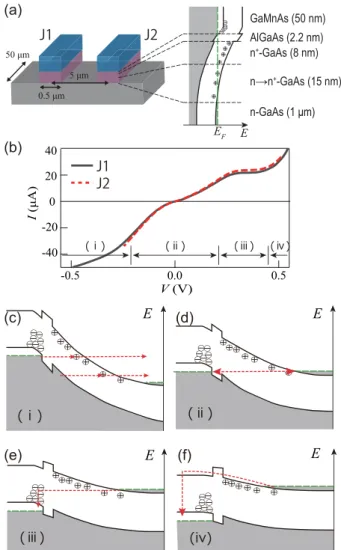
The detail of the sample fabrication is as follows. The epitaxial multilayer stack has been grown on a (001) GaAs substrate by a molecular beam epitaxy. It consists of a GaAs buffer, an AlGaAs/GaAs superlattice, a 1μmn-GaAs chan- nel, a 15-nm GaAs with linearly graded dopingn→n+(n= 2×1016cm−3 andn+=5×1018cm−3), an 8 nmn+−GaAs, a 2.2 nm low-temperature (LT)-grown AlGaAs, and a 50-nm LT-grown (Ga0.945Mn0.055)As. As shown in the right panel of Fig.1(a), due to the large difference in concentration of dopants, the depletion layer forms almost entirely on the GaAs side. The dopants and defects caused by the LT growth are considered to form LSs.
The wafer was patterned into 50-μm wide mesas along the [110] direction by standard photolithography and wet
(a)
(b)
I (μA)
V (V)
n-GaAs (1 μm) n→n+-GaAs (15 nm) n+-GaAs (8 nm) AlGaAs (2.2 nm) GaMnAs (50 nm)
-40 -20 0 20 40
-0.5 0.0 0.5
(c)
EF E
50 μm
0.5 μm 5 μm
(d) E
E (f) E
(e) E
FIG. 1. (a) Schematic illustration of our lateral spin valve devices with two spin Esaki junctions (J1 and J2). Right panel shows the band diagram of the (Ga,Mn)As/GaAs epitaxial multilayer stacks and energy of electrons. In the electron band diagram, the vertical dashed green line represents the Fermi energy. (b) Current-voltage (I-V) characteristics of each spin Esaki diode junctions. (c)–(f) Energy diagrams for several bias voltage conditions; the red dashed arrows sketch typical transport mechanisms, where (c), (d), (e), and (f) correspond to the bias regimes (i), (ii), (iii), and (iv) in (b), respectively.
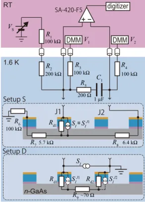
chemical etching. Then the ferromagnetic (Ga,Mn)As elec- trodes with a width of 0.5 µm were formed by electron beam lithography and reactive ion etching, where the etching process was stopped above then-GaAs channel layer. In this study, we used two junctions located in the center of the mesa, namely Junction 1 (“J1”) and Junction 2 (“J2”), with a size of 0.5 µm×50µm and a center-to-center distance of 5 µm, as shown in the left panel of Fig.1(a). Additionally, we used two large Esaki diode junctions of a size 150µm×150µm placed at the edges of the mesa, as reference contacts for electrical measurements [see Fig. 2]. Note that the top (Ga,Mn)As is a heavily doped p-type conductor, the interface between the Au/Ti electrode and (Ga,Mn)As forms an ohmic junction.
All the measurements were performed at a low temperature (1.6 K) to reduce thermal noise, using a variable temperature
1.6 K RT
DMM DMM
digitizer
R1 VS
n-GaAs
100 kΩ V1 V2
R2
200 kΩ
R3
100 kΩ
R4
100 kΩ
R5
200 Ω 1 μF
R6
100 kΩ Rd1
Rd2 Rd1
R7 R8
R9 SI
C1
SIJ1 SIJ2 SI
6.4 kΩ 5.7 kΩ
~70 Ω
SIJ1
=
FIG. 2. Schematics of the noise measurement setups including the equivalent circuit of the sample (see text for detail). By using a homemade sample holder, the low-temperature resistors and a capacitor are placed very close to the sample.
insert (Oxford Instrument plc.) equipped with a superconduct- ing magnet. Although an external magnetic field was applied parallel to the long axis of the ferromagnetic electrodes to sat- urate their magnetization along this direction, it was set to zero before the actual measurement was performed. Figure1(b) shows theI-Vcharacteristics of the J1 and J2 measured at 1.6 K using three-terminal configuration as explained in Sec.II B.
These two curves are almost identical. The nonlinear behavior, typical to the Esaki diode, is clearly pronounced. It consists of the following four regions (i, ii, iii, and iv) as shown in Figs.1(c),1(d),1(e), and1(f), respectively. At the large nega- tive bias region (i), nonlinearity appears due to the expansion of the depletion layer [Fig. 1(c)]. In region (ii) the direct tunneling between the valence band of (Ga,Mn)As and the conduction band ofn-GaAs [Fig.1(d)] dominates. The region (iii) is a so-called negative differential resistance region where the direct tunneling is forbidden [Fig.1(e)]. However, a clear dip, constituting a truly “negative” resistance, expected for an ideal Esaki diode, is not seen in the present spin Esaki diode.
This is due to the excess current through LSs as discussed below. Finally, (iv) is a region where the thermal excitation current across the built-in potential, as in conventional p-n junctions becomes dominant, resulting in a rapid increase of the current [Fig.1(f)].
B. Noise measurement
The equivalent circuit of our noise measurement system is shown in Fig. 2. In this study, electrical measurements were performed in two different experimental setups: single
junction (Setup S) and two junctions connected in series (Setup D) as shown in the bottom panel of Fig. 2. The
“sample” indicates J1 (Rd1) alone in Setup S, and the series circuit of J1 and J2 (Rd1+R9+Rd2) in Setup D, where Rd1 andRd2 are the differential resistance of the J1 and J2, respectively. Here we first describe the common parts. A dc bias current (I) is fed to the sample by using a programmable dc voltage source with the output voltage VS and two re- sistors (R1=100 k at RT and R2=200 k at 1.6 K).
The voltages (V1 and V2) across the sample were monitored by two digital multimeters, respectively. Here, I is deduced byI =(VS−V1)/(R1+R2) and the bias voltage (V) across the sample is given byV =V1−V2. Note that the reference voltages (V2) are measured at the right edge of the channel in Setup S and the contact on J2 in Setup D, respectively. We also measured the differential resistance at a given bias by modulatingIand measuringV in response.
The time domain voltage fluctuation signal was measured by a digitizer (National Instruments PCI-5922) after am- plification with a low-noise amplifier (NF Corporation SA- 420F5). Then, the voltage spectral densitySV was obtained by fast Fourier transformation (FFT). The resistances and the capacitance of the coaxial cables (∼300 pF in total) work as a low-pass filter. To increase the cutoff frequency, we useR5= 200 andC1 =1 μF at 1.6 K in parallel with the sample.
Moreover,R2,R3=100 kandR4=100 kare placed just near the sample to cut the capacitance of the coaxial cables that are connected to the RT measurement system. Here, since R5 is small compared to other resistances, it dominates the conversion from the current spectral density of the sample SI to SV. Thus, SV ≈G2R52SI where G is the gain of the amplifier. The frequency independent component of SV was estimated by fitting the spectrum taking the low-pass cutoff into account in the frequency range between 1.4 and 5 MHz.
In Setup S, SI is equal to the current noise generated by J1 (SI =SJ1I ). However, SV contains not only SI but also the thermal noise from the constant resistors (SIR5 =4kBT/R5
and SIR8=4kBT/R8), and other external current noise and voltage noise contributions (SIoffset andSVoffset) mainly due to the amplifier. The relation betweenSV andSI is given by
SV =G2
Rd1R5
Rd1+R5+R8
2
SI+
(Rd1+R8)R5 Rd1+R5+R8
2
×
SRI5+SoffsetI +
R5R8
Rd1+R5+R8 2
SRI8+SVoffset
.
(1) Since Rd1 varies depending on the bias voltage, two un- known variables (SIoffsetandSVoffset) are carefully calibrated.R7
andR8are the sums of the junction resistance of the reference contact at the left and the right edge of the mesa and the longitudinal resistance of the∼300-µm-long channel between the corresponding reference contact and J1, respectively. The large size of the reference contact, however, makes its resis- tance negligible compared to the channel resistance. Note that, withoutR6=100 k, the noise signalSI leaks to the ground side, resulting in a slight deviation from Eq. (1).
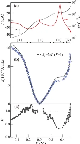
15
10
5
0
0.4 0.2 0.0 -0.2 -0.4 -40 -20 0 20 40
103 104 105 106
SI (10-24A2/Hz)I (μA) Rd1 (Ω)
V (V) (a)
(b)
F
1.0
0.9
0.8 (c)
SI =2eI (F=1)
FIG. 3. (a)IandRd1of junction J1 as a function of bias voltage.
(b) Measured SI in Setup S and calculated full-shot noise (2eI).
(c) EstimatedF(≡SI/2eI) by using the data in (b).
In the case of Setup D, SI is generated by the series circuit of J1, J2, andn-GaAs channel (Rd1+Rd2+R9 ≡Rd).
The relation betweenSV andSI of the series circuit is then expressed as
SV =G2
RdR5
Rd+R5
2
SI+SRI5+SIoffset +SVoffset
. (2) In the absence of spin accumulation in then-GaAs channel, one can expressSIof the series circuit based on the shot noise generated by each single junction. By usingRd1+Rd2 R9
and defining the current noise generated by J2 as SIJ2,SI is expressed as
SI =Rd12SIJ1+Rd22SJ2I
(Rd1+Rd2)2 . (3) III. RESULTS AND DISCUSSION
A. Single junction (Setup S)
Figure3(a)shows the bias voltage (V =V1−V2) depen- dence of I and Rd1 [the dotted curve is the same as shown in Fig.2(b)]. Applying a positive bias voltage,Rd1 gradually decreases, except for a peak in region (iii). This peak reflects the negative differential resistance and reaches its maximum around V ∼0.35V. For a negative bias, Rd1 first similarly decreases, and then increases in regions (i). As mentioned
above, full-shot noise (F =1) is expected for the Poissonian process in a conventional tunnel barrier. To see the difference from this value, the obtainedSI through Eq. (1) and calculated SI =2eI under the assumption that F =1 are plotted in Fig.3(b). In regions (ii) and (iv), the measured shot noise is in good agreement with the calculated curve, while reductions in SIare observed in regions (i) and (iii). To see these reductions more clearly, the bias voltage dependence of the estimated F(≡SI/2eI) is shown in Fig.3(c). In the region (ii),F is very close to unity, although the data points are scattered. On the other hand, in the region (iii),Fhas a broad dip structure with a local minimumF =0.87 atV ∼0.35V, which is in accord with the peak inRd1.
Let us focus on the transport properties in the region (ii). Since the direct tunnel process [see Fig. 1(d)] is sup- posed to be dominant in this region, our result (F ∼1) is not surprising. The experiments on germanium Esaki diodes [48,49] reported full-shot noise in this region. However, it is important to confirm the full-shot noise in the spin Esaki diode junction to evaluate the device quality. In fact, many types of deviation mechanisms from the full-shot noise limit have been studied both theoretically [1,9,10,16,22,24,43] and experimentally [7,11–14,17–19,23,25–27,50,51]. Our result ofF ∼1 indicates that the junction conductance in this bias region is purely governed by direct tunneling without leaking process such as sequential tunneling via defects.
In the previous paper [40], instead ofF =1.0, we reported F =0.78±0.04 in the region (ii) using the same device.
This difference in Fano factor is due to the measurement circuit, namely, the leakage of the noise signal through the ground loop was not well treated in the previous work [40].
This effect results in a systematic deviation in the noise signal, leading to the reported Fano factor less than 1. The important aspect here is the relative relationship between the resistance of the undesired parallel path via ground and the resistance of the signal line. In the present work, to prevent the leakage effect, we have inserted a large resistanceR6and choose a smaller resistance for R5, as shown in Fig. 2. R6
increases the resistance of the parallel path, while the smaller R5 decreases the resistance of the signal line. The proper combination of the used resistances has perfectly eliminated the artifact, enabling us to observe F ∼1.0 as expected.
Note that the difference in the absolute value of the Fano factor does not change at all the validity of the discussion in Ref. [40].
Next, we discuss the region (iv) where Rd1 rapidly de- creases in increasing ofV due to the influence of a thermal excitation current [see Fig.1(f)]. Although the noise signals are scattered, the average value of the Fano factor approaches F ∼1. This full-shot noise behavior has a different origin from that observed in region (ii). The thermal excitation current consists of the following processes. An electron is excited to the conduction band of (Ga,Mn)As by thermal ag- itation, followed by a radiative recombination after diffusion, as shown in Fig.1(f). This process is the same as in a usualp-n junction under forward bias. In this situation, full-shot noise is theoretically expected, as the thermal excitation and radiative recombination generate two-thirds and one-third of the full- shot noise, respectively. Thus full-shot noise is realized in total [52].
Now we discuss the mechanism of the reduced Fano factor in the region (iii). As direct tunneling is energetically pro- hibited here, electrons in the n-GaAs have to pass through LSs within the (Ga,Mn)As [30], as shown in Fig.1(e). In a germanium Esaki diode exhibiting a clear negative differential resistance, full-shot noise is reported in this region [48].
The present reduced Fano factor obtained in region (iii) is most likely due to LSs. The obtained Fano factor >0.87 is always larger than expected for a random distribution (F=3/4=0.75) [9], indicating that LSs are nonuniformly distributed. This is consistent with the concentration of dopants being much larger on the (Ga,Mn)As side than on the n-GaAs side, as shown in Fig. 1(e). The importance of the LSs for tunneling in (Ga,Mn)As spin Esaki diodes has been demonstrated also in other studies. Tunneling anisotropic magnetoresistance measurements on similar devices have shown the change of the transport mechanism between regions (ii) and (iii) [34]. Further, theI-Vcharacteristic of the present junction is well explained by theoretical work taking the impurity band in (Ga,Mn)As into account [41].
Finally, in the region (i), the reduction of the Fano factor can be explained as follows. The negative bias voltage widens the depletion layer [53], resulting in an increase of the contri- bution of sequential tunneling events, as shown in Fig.1(c).
In this region, only the LSs on then-GaAs side can contribute to the sequential process. Consequently, the reduction of the Fano factor is likely due to the sequential tunneling through the LSs in the depletion layer.
B. Double junction (Setup D)
In the Setup D, one has to distinguish between parallel (P) and antiparallel (AP) configurations of the relative mag- netization directions of the two ferromagnetic (Ga,Mn)As electrodes. In the AP configuration, the spin accumulation in the GaAs channel underneath and between ferromagnetic electrodes is typically much larger than in case of the P configuration [37]. Figure 4(a)shows theI-V characteristics for P and AP configurations (the left axis) and the differential resistance of each junction for P configuration (the right axis). AlthoughV shows a clear spin valve signal [33] in the magnetic field sweep, it is just 0.2% of the offset signal due to the large junction resistance. Hence, it is hard to see a difference in I-V characteristics between the P and AP configurations. In this study, the current polarity is defined as the forward direction for J1, which is the opposite direction for J2. Thus, the sign of the bias is opposite for the two junctions, and therefore the negative differential resistance region (iii) is achieved at aroundV = +0.5V and−0.5 V for J1 and J2, respectively. Note that when one junction is in the region (iii), the other is in the direct tunnel region (ii), as clearly seen in the right axis in Fig.4(a).
Figure4(b)shows the bias dependence of the obtainedSI
extracted from Eq. (2).SI is clearly the same for AP and P configurations, which indicates the negligibly small influence of the spin accumulation. Assuming the latter, we can now discuss the relation between SI in Setup D and Setup S.
Equation (3) indicates that SI depends on the quantitative balance betweenRd1 andRd2. Based on the result in Setup S, we first consider the situation that shot noise of each junction
10 8 6 4 2 0
-0.5 0.0 0.5
-20 0 20
104 105 106
SI (10-24A2/Hz)I (μA)
(a)
(b)
V (V) J1 J2 P
AP
P AP 1.0
0.75
0.5
F
(c)
Rd1 , Rd2 (Ω)
SI =2eI (F=1) SI =eI (F=1/2)
F=0.87
FIG. 4. (a) I-V characteristics of the junctions in series as a function of a bias voltage for parallel (P) and antiparallel (AP) configurations. The right axis showsRd1 and Rd2 of each junction for P configuration. (b) MeasuredSI in Setup D for P and AP. The solid and dashed lines show two shot noise limits. (c) Estimated F(≡SI/2eI) by using the data in (b).
exhibits the full-shot noise (SJ1I =SJ2I =2eI). As a result,SI
in the series junction is expected to beeIfor Rd1∼Rd2 and 2eI forRd1 Rd2 orRd1Rd2. In Fig.4(b), the measured SI is compared with these two limits, namely, a solid line for SI =2eIand a broken line forSI =eI. Except for the strong asymmetric case due to the negative differential resistance regions around V = ±0.5 V, SI matches the broken line.
This result indicates full-shot noise in region (ii), which is consistent with the result for Setup S.
In order to see it more clearly, the bias voltage dependence of the estimatedF(≡SI/2eI) is plotted in Fig.4(c). Here, the two limits yieldF =1/2 forRd1 ∼Rd2[horizontal dotted line in Fig.4(c)] andF =1 forRd1Rd2orRd1Rd2. It is clear that the curves are in good agreement with theF =1/2 line except aroundV = ±0.5 V. For these voltages the maximum values ofF are clearly smaller than unity. Now, defining the Fano factor of J1 and J2 junctions asF1 andF2, respectively,
we obtain the relations:F =F1forRd1 Rd2andF =F2for Rd1Rd2. Indeed, the maximum values of theF peaks agree with value ofF1(=0.87) obtained in region (iii) of Setup S, as shown in Fig.4(c)as a horizontal solid line. These results indicate that Setup S and Setup D show consistent results.
The present series circuit consists of a nonmagnetic chan- nel sandwiched by two ferromagnetic materials through a tun- nel barrier. The shot noise in such a system has been studied theoretically [54,55], indicating that the Fano factor depends on the magnetic configuration. In fact, experimental studies on layered double-barrier magnetic tunnel junctions report magnetic configuration dependent shot noise and discuss spin relaxation in the middle layer [56,57]. However, no significant difference of the Fano factor between P and AP configurations was detected in the present study. In our lateral device, the spin accumulation in the n-GaAs channel is energetically small compared to the voltage drop across J1 and J2, thus too small to affect the tunneling current across the junctions.
IV. CONCLUSION
We measured shot noise properties of (Ga,Mn)As/GaAs- based spin Esaki diode junctions over a wide bias voltage range. We have clarified that transport through the Esaki junc-
tion changes dramatically depending on an applied bias. In the low bias voltage regime, full-shot noise (F =1) associated with direct tunneling was observed. This was also observed in the large positive bias region, resulting from recombina- tion of the thermal diffusion current. On the other hand, we observed the reduced Fano factor in the negative differential resistance region and in the large negative bias region. These reductions can be explained by taking the excess current via LSs into consideration. In addition, we also measured shot noise of a series circuit of two spin Esaki diode junctions in a lateral geometry and obtained consistent results for the single junction and double junction cases. Our findings of bias dependence of the Fano factor in the Esaki diode junction provide an important information for in-depth understanding of the transport mechanism in the presence of the LSs.
ACKNOWLEDGMENTS
This work was supported by JSPS KAKENHI Grants No. JP18H01815, No. JP16H05964, No. JP19H00656, No.
JP15H05699, and No. JP19H05826. We also acknowledge funding by the Deutsche Forschungsgemeinschaft (DFG) via the Collaborative Research Center SFB 689.
[1] Y. M. Blanter and M. Büttiker, Shot noise in mesoscopic conductors,Phys. Rep.336, 1 (2000).
[2] Y. V. Nazarov, Limits of Universality in Disordered Conductors, Phys. Rev. Lett.73, 134 (1994).
[3] K. M. Schep and G. E. W. Bauer, Universality of Transport Through Dirty Interfaces,Phys. Rev. Lett.78, 3015 (1997).
[4] H. U. Baranger and P. A. Mello, Mesoscopic Transport Through Chaotic Cavities: A Random s-Matrix Theory Approach, Phys. Rev. Lett.73, 142 (1994).
[5] W. Schottky, Über spontane stromschwankungen in verschiede- nen elektrizitätsleitern,Ann. Phys.362, 541 (1918).
[6] L. Spietz, K. W. Lehnert, I. Siddiqi, and R. J. Schoelkopf, Primary electronic thermometry using the shot noise of a tunnel junction,Science300, 1929 (2003).
[7] Y. Chen and R. A. Webb, Full shot noise in mesoscopic tunnel barriers,Phys. Rev. B73, 035424 (2006).
[8] A. B. Fowler, G. L. Timp, J. J. Wainer, and R. A. Webb, Observation of Resonant Tunneling in Silicon Inversion Layers, Phys. Rev. Lett.57, 138 (1986).
[9] Y. V. Nazarov and J. J. R. Struben, Universal excess noise in resonant tunneling via strongly localized states,Phys. Rev. B 53, 15466 (1996).
[10] L. Y. Chen and C. S. Ting, Noise characteristics of sequential tunneling through double-barrier junctions, Phys. Rev. B 46, 4714 (1992).
[11] P. Ciambrone, M. Macucci, G. Iannaccone, B. Pellegrini, M.
Lazzarino, L. Sorba, and F. Beltram, Noise measurements in resonant tunnelling structures as a function of current and temperature,Electron. Lett.31, 503 (1995).
[12] H. C. Liu, J. Li, G. C. Aers, C. R. Leavens, M. Buchanan, and Z. R. Wasilewski, Shot-noise suppression in resonant tunneling, Phys. Rev. B51, 5116 (1995).
[13] A. Przadka, K. J. Webb, D. B. Janes, H. C. Liu, and Z. R.
Wasilewski, Microwave measurement of shot noise in resonant tunneling diodes,Appl. Phys. Lett.71, 530 (1997).
[14] R. Guerrero, F. Aliev, Y. Tserkovnyak, T. Santos, and J.
Moodera, Shot Noise in Magnetic Tunnel Junctions: Evidence for Sequential Tunneling,Phys. Rev. Lett.97, 266602 (2006).
[15] I. Maione, M. Macucci, G. Iannaccone, G. Basso, B. Pellegrini, M. Lazzarino, L. Sorba, and F. Beltram, Probing Pauli blocking with shot noise in resonant tunneling diodes: Experiment and theory,Phys. Rev. B75, 125327 (2007).
[16] G. Iannaccone, F. Crupi, B. Neri, and S. Lombardo, Theory and experiment of suppressed shot noise in stress-induced leakage currents,IEEE Trans. Electron Devices50, 1363 (2003).
[17] V. V. Kuznetsov, E. E. Mendez, J. D. Bruno, and J. T. Pham, Shot noise enhancement in resonant-tunneling structures in a magnetic field,Phys. Rev. B58, R10159 (1998).
[18] S. S. Safonov, A. K. Savchenko, D. A. Bagrets, O. N. Jouravlev, Y. V. Nazarov, E. H. Linfield, and D. A. Ritchie, Enhanced Shot Noise in Resonant Tunneling via Interacting Localized States, Phys. Rev. Lett.91, 136801 (2003).
[19] T. Tanaka, T. Arakawa, M. Maeda, K. Kobayashi, Y. Nishihara, T. Ono, T. Nozaki, A. Fukushima, and S. Yuasa, Leak current estimated from the shot noise in magnetic tunneling junctions, Appl. Phys. Lett.105, 042405 (2014).
[20] Y. Kim, H. Song, T. Lee, and H. Jeong, Shot noise suppression in sige resonant interband tunneling diodes,Jpn. J. Appl. Phys.
47, 8752 (2008).
[21] Y. Xu, D. Ephron, and M. R. Beasley, Directed inelastic hop- ping of electrons through metal-insulator-metal tunnel junc- tions,Phys. Rev. B52, 2843 (1995).
[22] A. N. Korotkov and K. K. Likharev, Shot noise suppression at one-dimensional hopping,Phys. Rev. B61, 15975 (2000).
[23] V. V. Kuznetsov, E. E. Mendez, X. Zuo, G. L. Snider, and E. T. Croke, Partially Suppressed Shot Noise in Hopping Con- duction: Observation in SiGe Quantum Wells,Phys. Rev. Lett.
85, 397 (2000).
[24] V. A. Sverdlov, A. N. Korotkov, and K. K. Likharev, Shot- noise suppression at two-dimensional hopping,Phys. Rev. B63, 081302 (2001).
[25] F. E. Camino, V. V. Kuznetsov, E. E. Mendez, M. E.
Gershenson, D. Reuter, P. Schafmeister, and A. D. Wieck, Hopping conductivity beyond the percolation regime probed by shot-noise measurements,Phys. Rev. B68, 073313 (2003).
[26] A. K. Savchenko, S. S. Safonov, S. H. Roshko, D. A. Bagrets, O. N. Jouravlev, Y. V. Nazarov, E. H. Linfield, and D. A.
Ritchie, Shot noise as a probe of electron transport via localised states in sub-micrometer barriers, Phys. Status Solidi B242, 1229 (2005).
[27] R. Danneau, F. Wu, M. Y. Tomi, J. B. Oostinga, A. F. Morpurgo, and P. J. Hakonen, Shot noise suppression and hopping con- duction in graphene nanoribbons, Phys. Rev. B 82, 161405 (2010).
[28] E. S. Tikhonov, V. S. Khrapai, D. V. Shovkun, and D.
Schuh, Finite-size effect in shot noise in hopping conduction, JETP Lett.98, 121 (2013).
[29] L. Esaki, New phenomenon in narrow germaniump-njunctions, Phys. Rev.109, 603 (1958).
[30] A. Chynoweth, W. Feldmann, and R. Logan, Excess tun- nel current in silicon Esaki junctions, Phys. Rev. 121, 684 (1961).
[31] M. Kohda, Y. Ohno, K. Takamura, F. Matsukura, and H. Ohno, A spin Esaki diode,Jpn. J. Appl. Phys.40, L1274 (2001).
[32] M. Ciorga, A. Einwanger, U. Wurstbauer, D. Schuh, W.
Wegscheider, and D. Weiss, Electrical spin injection and de- tection in lateral all-semiconductor devices,Phys. Rev. B79, 165321 (2009).
[33] J. Shiogai, M. Ciorga, M. Utz, D. Schuh, M. Kohda, D.
Bougeard, T. Nojima, J. Nitta, and D. Weiss, Giant enhance- ment of spin detection sensitivity in (Ga,Mn)As/GaAs Esaki diodes,Phys. Rev. B89, 081307 (2014).
[34] J. Shiogai, M. Ciorga, M. Utz, D. Schuh, M. Kohda, D.
Bougeard, T. Nojima, D. Weiss, and J. Nitta, In-plane tunnel- ing anisotropic magnetoresistance in (Ga,Mn)As/GaAs Esaki diodes in the regime of the excess current,Appl. Phys. Lett.
106, 262402 (2015).
[35] M. Oltscher, M. Ciorga, M. Utz, D. Schuh, D. Bougeard, and D.
Weiss, Electrical Spin Injection into High Mobility 2D Systems, Phys. Rev. Lett.113, 236602 (2014).
[36] M. Ciorga, Electrical spin injection and detection in high mo- bility 2DEG systems, J. Phys.: Condens. Matter 28, 453003 (2016).
[37] M. Oltscher, F. Eberle, T. Kuczmik, A. Bayer, D. Schuh, D. Bougeard, M. Ciorga, and D. Weiss, Gate-tunable large magnetoresistance in an all-semiconductor spin valve device, Nat. Commun.8, 1807 (2017).
[38] J. Shiogai, M. Ciorga, M. Utz, D. Schuh, T. Arakawa, M. Kohda, K. Kobayashi, T. Ono, W. Wegscheider, D.
Weiss, and J. Nitta, Dynamic nuclear spin polarization in an all-semiconductor spin injection device with (Ga,Mn)As/n- GaAs spin Esaki diode, Appl. Phys. Lett. 101, 212402 (2012).
[39] J. Shiogai, M. Ciorga, M. Utz, D. Schuh, M. Kohda, D.
Bougeard, T. Nojima, D. Weiss, and J. Nitta, Spatial variation of dynamic nuclear spin polarization probed by the non-local Hanle effect,Appl. Phys. Lett.112, 132403 (2018).
[40] T. Arakawa, J. Shiogai, M. Ciorga, M. Utz, D. Schuh, M.
Kohda, J. Nitta, D. Bougeard, D. Weiss, T. Ono, and K.
Kobayashi, Shot Noise Induced by Nonequilibrium Spin Ac- cumulation,Phys. Rev. Lett.114, 016601 (2015).
[41] P. Pereyra and D. Weiss, Exchange energy and impurity band effects in the I−V characteristics of (Ga,Mn)As/GaAs spin injectors,Phys. Rev. B90, 245310 (2014).
[42] F. Aliev and J. P. Cascales, Noise in Spintronics: From Un- derstanding to Manipulation, 1st ed. (Taylor and Francis, New York, 2018).
[43] F. M. Souza, J. Del Nero, and J. C. Egues, Shot noise in a spin- diode geometry,J. Supercond. Nov. Magn.23, 45 (2009).
[44] F. J. Jedema, H. B. Heersche, A. T. Filip, J. J. Baselmans, and B. J. van Wees, Electrical detection of spin precession in a metallic mesoscopic spin valve, Nature (London) 416, 713 (2002).
[45] X. Lou, C. Adelmann, S. A. Crooker, E. S. Garlid, J. Zhang, K. S. M. Reddy, S. D. Flexner, C. J. Palmstrøm, and P.
A. Crowell, Electrical detection of spin transport in lateral ferromagnet–semiconductor devices,Nat. Phys.3, 197 (2007).
[46] H. C. Koo, J. H. Kwon, J. Eom, J. Chang, S. H. Han, and M. Johnson, Control of spin precession in a spin-injected field effect transistor,Science325, 1515 (2009).
[47] Y. Niimi, D. Wei, and Y. Otani, Effect of magnetic fluctuations on spin current,J. Phys. Soc. Jpn.86, 011004 (2016).
[48] J. J. Tiemann, Shot noise in tunnel diode amplifiers,Proc. IRE 48, 1418 (1960).
[49] A. Yariv and J. S. Cook, A noise investigation of tunnel-diode microwave amplifiers,Proc. IRE49, 739 (1961).
[50] T. Arakawa, K. Sekiguchi, S. Nakamura, K. Chida, Y.
Nishihara, D. Chiba, K. Kobayashi, A. Fukushima, S. Yuasa, and T. Ono, Sub-Poissonian shot noise in CoFeB/MgO/CoFeB- based magnetic tunneling junctions, Appl. Phys. Lett. 98, 202103 (2011).
[51] T. Tanaka, T. Arakawa, K. Chida, Y. Nishihara, D. Chiba, K.
Kobayashi, T. Ono, H. Sukegawa, S. Kasai, and S. Mitani, Sig- nature of coherent transport in epitaxial spinel-based magnetic tunnel junctions probed by shot noise measurement,Appl. Phys.
Express5, 053003 (2012).
[52] M. J. Buckingham,Noise in Electronic Devices and Systems (Prentice Hall, Upper Saddle River, NJ, 1983).
[53] S. M. Sze, Semiconductor Devices: Physics and Technology (Wiley, New York, 1986), Chap. 4.
[54] Y. Tserkovnyak and A. Brataas, Shot noise in ferromagnet–
normal metal systems,Phys. Rev. B64, 214402 (2001).
[55] E. G. Mishchenko, Shot noise in a diffusive ferromagnetic- paramagnetic-ferromagnetic spin valve, Phys. Rev. B 68, 100409 (2003).
[56] T. Szczepa´nski, V. Dugaev, J. Barna´s, J. Cascales, and F.
Aliev, Shot noise in magnetic double-barrier tunnel junctions, Phys. Rev. B87, 155406 (2013).
[57] J. P. Cascales, D. Herranz, F. G. Aliev, T. Szczepanski, V. K.
Dugaev, J. Barnas, A. Duluard, M. Hehn, and C. Tiusan, Controlling Shot Noise in Double-Barrier Magnetic Tunnel Junctions,Phys. Rev. Lett.109, 066601 (2012).