Graphene www.ann-phys.org
Terahertz Electric Field Driven Electric Currents and Ratchet Effects in Graphene
Sergey D. Ganichev,* Dieter Weiss, and Jonathan Eroms
Terahertz field induced photocurrents in graphene were studied
experimentally and by microscopic modeling. Currents were generated bycw and pulsed laser radiation in large area as well as small-size exfoliated graphene samples. We review general symmetry considerations leading to photocurrents depending on linear and circular polarized radiation and then present a number of situations where photocurrents were detected. Starting with the photon drag effect under oblique incidence, we proceed to the photogalvanic effect enhancement in the reststrahlen band of SiC and edge-generated currents in graphene. Ratchet effects were considered for in-plane magnetic fields and a structure inversion asymmetry as well as for graphene with non-symmetric patterned top gates. Lastly, we demonstrate that graphene can be used as a fast, broadband detector of terahertz radiation.
1. Introduction
The advent of graphene and topological insulators (TI) started a new research direction in materials science. A distinctive fea- ture of these materials is that their band structure resembles the dispersion relation of a massless relativistic particle being de- scribed by the Dirac equation. Transport effects linear in elec- tric field have been studied extensively in those materials, lead- ing to significant progress both in basic research and a number of applications (see, e.g., Refs. [1–6] for a review). Unique opti- cal properties of this material also caused a rapid development of graphene photonics and optoelectronics, see e.g., Refs. [7–9].
Nonlinear transport effects, being proportional to higher powers of the field, offer a new playground for many interesting phenom- ena in the physics of Dirac fermions (DF).[10] These effects are usually caused by the radiation induced redistribution of charge carriers in momentum/energy space and reconstruction of the energy spectra. The resulting response comprises components which oscillate in time and space, but also has a steady-state and spatially uniform contributions. Therefore, bothac anddccur- rents are generated, consisting of terms whose magnitudes de- pend nonlinearly on the field amplitude and which are controlled by the radiation polarization.
Edge and bulk photocurrents have been detected in many DF systems excited by infrared/terahertz radiation, giving Sergey D. Ganichev, Dieter Weiss, Jonathan Eroms
Terahertz Center University of Regensburg 93040 Regensburg, Germany
E-mail: sergey.ganichev@physik.uni-regensburg.de DOI: 10.1002/andp.201600406
insights into the microscopic mecha- nisms and the requirements for such kind of experiments. Focusing on DFs in graphene, some recent theoretical and experimental examples of such phenomena include the circular dy- namic Hall effect,[11,12] circular and linear photogalvanic effects,[12–14] chi- ral edge photocurrents,[15] coherent current injection,[16–18] magnetic quan- tum ratchet,[19] ratchet effects with lateral potential,[20] and time-resolved photocurrents.[21–24] For a review on nonlinear electron transport in bulk graphene at B=0 see Ref. [10]. These studies demonstrate substantial differ- ences of the microscopic mechanisms of nonlinear transport effects in DF systems and conventional semi- conductors. Thus, the experimental and theoretical research in the field of nonlinear optics and optoelectronics in DF in in- frared/terahertz spectral range becomes already an important task, for reviews see Refs. [10,25–29]. Furthermore, infrared/THz spectroscopy turns out to be an efficient tool providing informa- tion on band parameters, Fermi velocity, symmetry properties, carrier dynamics, etc. From an application point of view, convert- ing anacelectric THz field into adccurrent is a very promising route towards fast, sensitive detection of terahertz radiation at room temperature.[23,24]
In this feature article, we will focus on the effects of the lower- ing of symmetry by various mechanisms on photo-induced cur- rents in graphene. Due to the high symmetry of graphene, such signals are forbidden for normal incidence of the electromag- netic radiation. By changing the angle of incidence or lowering the symmetry, signals are obtained. We will give an overview of the terahertz radiation induced photocurrents in graphene, de- scribe principal experimental and theoretical findings of nonlin- ear physics in graphene and suggest further studies in this re- search area. We will first briefly introduce the methods used to study nonlinear phenomena in graphene. Then, in Sections 3-5 we describe photocurrents generated in pristine graphene and at graphene edges. In Secs. 6-7 we address ratchet effects in graphene. We begin with ratchet effects generated by the ap- plication of an external magnetic field being caused by the pe- riodic radiation field and structure inversion asymmetry. Then we describe ratchet effects in graphene superimposed with peri- odic asymmetric lateral potential. For each effect, we will proceed in the following way: We present symmetry arguments allow- ing a phenomenological analysis of the respective phenomena, then outline the microscopic theory and finally discuss the main
experimental findings. In Sec. 8 we discuss the application of graphene photoelectrical phenomena for fast room temperature detection of infrared/terahertz radiation. Finally, in Sec. 9 we summarize the results and discuss the prospects of future theo- retical and experimental studies of the nonlinear electromagnetic response of graphene.
2. Methods
2.1. Symmetry Analysis
Photocurrents discussed in this paper are phenomenologically described by writing the current as an expansion in powers of the electric field E=E(ω) exp (−iωt)+c.c.at the frequencyωand the wavevectorqof the radiation field inside the medium.[10,30–33]
The lowest order nonvanishing terms yielding adccurrent den- sity jare given by
jλ=
μ,ν
χλμνEμE∗ν+
δ,μ,ν
TλδμνqδEμEν∗, (1)
where Eν∗=E∗ν(ω)=Eν(−ω) is the complex conjugate of Eν. The expansion coefficients χλμν and Tλμνδ are third rank and fourth rank tensors, respectively. The first term on the right-hand side of Eq. (1) represents photogalvanic (PGE) effects. The sec- ond term containing the wavevector of the electromagnetic field describes the photon drag (PDE) effect. Both effects are sensi- tive to the radiation polarization which is defined by the varia- tion of product EμEν∗. In general both, photogalvanic and pho- ton drag effect, yield photocurrents depending on the degree of linear polarization and on the radiation helicity as well as have a contribution being independent of the radiation polarization.
Taking the example of the photogalvanic effects, we obtain the photocurrent contributions attributed to the action of linearly and circularly polarized radiation. The bilinear combination EμEν∗ can be rewritten as a sum of a symmetric and an antisymmetric product
EμEν∗= {EμE∗ν} +[EμE∗ν], (2) with
{EμEν∗} = 1
2(EμEν∗+EνE∗μ) (3)
and [EμE∗ν]= 1
2(EμEν∗−EνEμ∗). (4)
This decomposition of EμEν∗corresponds to a splitting into real and imaginary parts. Due to contraction of the tensorχλμν withEμEν∗the same algebraic symmetries are projected onto the last two indices ofχλμν. The real part ofχλμνis symmetric in in- dicesμνwhereas the imaginary part is antisymmetric. Antisym- metric tensor index pairs can be reduced to a single pseudovec- tor index using the Levi–Civita totally antisymmetric tensorδρμν.
Applying this simplification we obtain for the current due to the antisymmetric part ofEμE∗ν
χλμν[EμEν∗]=i·
ρ
γλρδρμν[EμEν∗]=γλρi(E×E∗)ρ, (5)
with the real second rank pseudotensorγλρ andi(E×E∗)ρ= ˆeρPcircE2, where ˆe=q/q,PcircandE2= |E(ω)|2are the unit vec- tor pointing in the direction of light propagation, degree of light circular polarization (helicity) and the radiation intensity, respec- tively. In summary we find for the total photogalvanic current
jλPGE=
μ,ν
χλμν{EμEν∗} +
ρ
γλρi(E×E∗)ρ, (6)
whereχλμν=χλνμ. In this equation the photogalvanic effect is decomposed into the LPGE (linear photogalvanic effect) and the CPGE (circular photogalvanic effect) described by the first and second term on the right-hand side, respectively. The correspond- ing contributions for the photon drag current can be obtained in a similar way.
Linear and circular photogalvanic and photon drag currents have been observed in various semiconductors and are theoreti- cally well understood (for reviews see, e.g., Refs. [10,30–37]).
Symmetry analysis permits us to describe the various effects and their observability in terms of macroscopic parameters, such as radiation intensity, polarization and angle of incidence with- out detailed knowledge of the microsopic origin. Disregarding the substrate, a homogeneous, infinite pristine graphene layer belongs to the centrosymmetricD6hpoint group. When a sub- strate or asymmetrically placed adatoms are present, the sym- metry is reduced to the the noncentrosymmetric groupC6v, re- moving the equivalence of thezand−zdirections. While the photon drag effect can be detected for both kinds of graphene structures photogalvanic effects, which require the lack of inver- sion symmetry, can not be excited in an infinite homogeneous pristine graphene layer. Symmetry analysis shows that photocur- rents in the graphene systems addressed above can be gener- ated for oblique incidence only and may have a contribution along radiation propagation and normal to it, seeFigure 1(a) and (b). However, in real structures photocurrents excited by perpen- dicularly incident radiation may become become possible, e.g.
when the edges are illuminated, see Figure 1(c), and symme- try is reduced locally, or in samples with ripples or terraces. The photocurrent at normal incidence may further become possible for graphene with asymmetric metal structures on its top, see Figure 1(d), or when an plane static magnetic field is applied.
Since second-order phenomena are sensitive to spatial inver- sion, particular properties of the samples, like the presence of adatoms, terraces, ripples and edges, or the coupling to the sub- strate become important.
Furthermore, those effects depend strongly on angle of inci- dence and the radiation polarization. Studying of these depen- dencies, together with the symmetry analysis, helps to explore microscopic mechanisms responsible for the photocurrent gen- eration. Our works demonstrate that the various possible con- tributions to the nonlinear response are just proportional to the Stokes parameters, which describe the polarization state of radiation. Hence, when performing measurements of nonlinear
Figure 1. Measurement configurations for the detection of longitudinal (a) and transverse (b) photocurrents. The plane of incidence of the radiation is also defined. Black dots: Contacts to graphene. (c) and (d) demonstrate illumination with circularly and linearly polarized light.
high frequency effects in graphene, we vary the radiation polar- ization state by rotating standard dichroic elements likeλ/2 and λ/4 plates or Fresnel rhombs with respect to the polarization plane of the linearly polarized laser radiation with (El x). For light propagating in the direction of the positivezaxis, the Stokes parameters[38,39]are given by
S1= |Ex|2− |Ey|2
|Ex|2+ |Ey|2 ∝cos 2α∝cos22ϕ, (7) S2= ExE∗y+Ex∗Ey
|Ex|2+ |Ey|2 ∝sin 2α∝sin 4ϕ, (8) S3≡Pcirc=iExE∗y−E∗xEy
|Ex|2+ |Ey|2 =sin 2ϕ , (9) where|Ex|2+ |Ey|2defines the radiation intensity,α=2βis the azimuth angle defining the orientation of the polarization plane for linearly polarized radiation andβandϕare the angles be- tweenEl the optical axiscfor half- and quarter wave elements, respectively.
2.2. Experimental
Photocurrents in graphene have been observed and studied ap- plying radiation from near- up to very far-infrared range. To cover a wide frequency range, stretching over three decades from fractions- up to tens of terahertz, various radiation sources have been applied including molecular optically pumpedcwand pulsed lasers at Regensburg Terahertz Center (for laser char- acteristics see, e.g., Refs. [40–45]), free electron lasers Felbe in Rossendorf[23,24,46,47] and Felix in the Netherlands,[48,49] tunable CO2 lasers,[33] quantum cascade lasers[50–52]and backward wave oscillators.[53]Using of various sources of radiation not only al- lowed to explore frequency dependencies of the photocurrents under study, but also made possible demonstration of robustness to high radiation power and examination of the subnanosecond photocurrent dynamics. We emphasize that the photocurrents are detectable at very low power of microWatts and yield response linearly scaling with radiation power up to at least 100 kW with- out samples damage.
The main experimental geometries used for these studies are outlined in Figure 1. We illuminated the graphene samples un- der normal or oblique incidence, with the incidence angle θ0
varying from−40◦to+40◦. The photocurrents have been mea- sured as a voltage drop across a load resistance, RL. For experi- ments with pulsed lasers the photovoltage signal,V, was detected by a digital oscilloscope and forcwradiation modulated with a
chopper by using standard lock-in technique. While for the mea- surements applying pulsed lasers with nanoseconds pulse du- ration RL=50 Ohm has been used for cwradiation in some cases much higher load resistance have been used as well. In the former set-up the photocurrentIrelates to the photovoltage VasI=V/RL, because in all experiments described below the load resistance was much smaller than the sample resistanceRS
(RLRS). The corresponding photocurrent density is obtained as j =I/w, wherewis the width of the graphene sample. The latter configuration greatly increases the magnitude of the volt- age signal but complicates the analysis for the case when sam- ple resistance varies substantially with an external parameter, e.g magnetic field or gate voltage. The radiation was focused onto the samples by a parabolic mirror and its powerPwas controlled by photon drag and pyroelectric detectors. The beam shape of the THz radiation is almost Gaussian, measured with a pyroelectric camera.[54,55]
Photocurrents of different microscopic origins have been ob- served in a large temperature range from 2 up to 300 K. We emphasize that all observed photocurrents have been also de- tected at technologically important room temperature. While studying of the temperature dependence also played an im- portant role for understanding the photocurrent formation the largest portion of the research was focused on room temperature response.
2.3. Samples
Terahertz radiation induced photocurrents have been observed and studied in graphene samples prepared applying different technologies including: (i) epitaxial graphene prepared by high temperature Si sublimation of semi-insulating silicon carbide (SiC) substrates,[56–62](ii) CVD graphene grown in a conventional chemical vapor deposition process using copper as substrate and catalyst and methane as carbon source[19]and (iii) exfoliated graphene[63]deposited on oxidized silicon wafers. Details on the growth and characterization of material used for photocurrent studies can be found in Refs. [11,15,19,20,23,24,58,60–62]. The technologies (i) and (ii) allowed us to prepare large area samples with 5×5 mm2graphene monolayers while the size of the exfoli- ated structures was in the range of tens of micrometers. The large size of the epitaxial and CVD samples was of particular impor- tance for the analysis of the photocurrent formation. While both large and small size samples showed the effects, the response of the micron sized exfoliated samples in all type of experiments had an unavoidable contribution of the edge photocurrents dis- cussed in Sec. 5. This is because the spot size of the terahertz laser of about 1 mm2is much larger than the graphene flakes.
Most experiments were carried out onn- andp-type layers with carrier concentrations in the range of (0.5 to 7)×1012cm−2, Fermi energy EF of several hundreds of meV, and mobilities about 1000 cm2/Vs at room temperature. We note that in all photocur- rent experiments described below were performed in the limit ωEF. Thus microscopic theory of the studied phenomena has been developed for theclassicalregime of light-matter interac- tion. Thus a microscopic description of each photocurrent under study was obtained by solving the Boltzmann kinetic equation for the electron distribution function f(p,r,t). Here pis the free- carrier momentum,ris the in-plane coordinate andtis time.
Electron transport parameters have been obtained from magneto-transport measurements. For some experiments, e.g.
on terahertz ratchet effects described in Sec. 7, concentration and type of carriers have been controllably changed applying top and back gate voltages.
To obtain defined graphene edges an edge trim of about 200μm width was removed by reactive ion etching with an ar- gon/oxygen plasma. To protect graphene from uncontrollable change of transport parameters most of samples were encapsu- lated in a polymer film,[61]consisting of PMMA/MAA thin film followed by ZEP520 polymer. The unprotected samples were sub- ject to contamination from the ambient atmosphere. The latter has been seen from the change in carrier mobility and density on a time scale of months.
For electrical measurements eight contacts were made in the corners and at the middle of the sides of the square shaped large size graphene layer. The contacts have been fabricated by e-beam deposition of 3 nm Ti and 80 nm Au using a laser-cut shadow mask. Each of the electrodes had 200x200μm2lateral dimension.
Raman spectra taken from several points of each of the samples showed high crystallinity, 1-2 atomic layer thick graphene. Metal contacts to graphene flake has been prepared on the periphery of graphene applying standard lithographic deposition of Ti/Au (3/100 nm) and lift-off.
For studying ratchet effects, metal film superlattices were fab- ricated on large area epitaxial graphene as well as on small area flakes. A sketch of the superlattices gate fingers and a correspond- ing optical micrograph are presented in Sec. 7. Preparing gates, first, an insulating aluminium oxide layer was deposited on top of the graphene sheet. The lateral periodic electrostatic potential is created on top of epitaxial graphene by periodic grating-gate fingers fabricated by electron beam lithography and subsequent deposition of metal. On small area graphene flakes we fabricated inter-digitated metal-grating gates TG1 and TG2 having different stripe width and stripe separation. This allowed us to apply dif- ferent bias voltages to the individual subgrating gates forming the superlattice. The samples were glued onto holders with con- ductive epoxy utilizing the highly doped silicon wafer as a back gate which enabled us to change type and density of free carriers in graphene. Contact pads were placed in a way that the photo- induced currents can be measured parallel and perpendicular to the metal fingers.
3. Photon Drag Effect
We demonstrated the photon drag effect in graphene produced both by exfoliation and epitaxial techniques[10–13]under oblique
incidence of radiation. Electric currents were obtained both in the direction of the radiation propagation (longitudinal geome- try) as well as perpendicular to it (transverse geometry). Using the Boltzmann kinetic equation we obtain a microscopic descrip- tion of the photon drag:
∂f
∂t +v∂f
∂r +e(E+v×B)∂f
∂p=Q{f}. (10)
Here,v=dε/dpis the velocity,εis the kinetic energy, andQ{f} is the collision integral described in terms of relaxation timesτn
(n=1,2. . .) for corresponding angular harmonics of the distri- bution function.[10,12,64] The electric current density is given by the standard equation
j =4e
p
v f(p), (11)
wheree is the electron charge and a factor of 4 accounts for spin and valley degeneracies. We expand the distribution func- tion in powers of electric and magnetic fields, retaining linear and quadratic terms only. Calculations of f(p) and j are car- ried out using the energy dispersionεp= ±vpof free carriers in graphene and the relationv≡vp=vp/|p|between the velocity and the quasi-momentum (v≈c/300, withcbeing the speed of light). The photon drag current can be generated either due to combined action of the electric and magnetic field of the electro- magnetic wave (E B-mechanism or the dynamic Hall effect) or due to the spatial gradient of the in-plane projection of the ra- diation electric field (q E2-mechanism). Since in plane waves the complex amplitudes of electric and magnetic fields in Eq. (10) are coupled,B(ω,q)= c|q|1 [q×E(ω,q)] (taking0=1 andμ0=1), both mechanisms share the same origin. Therefore, the dynamic Hall effect∝EβBγ∗can be expressed in terms of the photon drag effect, i.e.∝qδEβE∗γ. When the effect is treated microscopically in terms of the number of photons (quantum mechanical pic- ture), we speak of the photon drag effect, while the classical pic- ture using the action of electromagnetic fields results in the term dynamic Hall effect.
The model of the dynamic Hall effect excited by linearly polar- ized radiation is illustrated inFigure 2(a). At one given moment in time,t1, the Lorentz force caused by the radiation electric and magnetic fields results in a drift in the direction of the light prop- agation. Half a radiation period later, at timet2, both fields have changed their sign, therefore, the drift direction remains. Aver- aging over time, this leads to a time-independent Hall current with fixed direction. The latter depends on the electric field vec- tor orientation and is odd in the angle of incidence,θ0. The ad- ditional contribution caused by theq E2-mechanism is also odd inθ0and vanishes for normal incidence. The terms of the fourth- rank tensorTαβγ μwhich are symmetric and antisymmetric under βγ ↔γβ, yield a photon drag contribution responding to lin- early and circularly polarized radiation, respectively (in short: lin- ear and circular photon drag effects).[65–68]While the longitudinal current can be understood intuitively for arbitrary polarization, the transverse current obtained by circularly polarized radiation is not obvious. It changes its sign upon reversing the helicity of the radiation, and retardation the electric fieldEand the instant velocity of charge carriervhas to be taken into account.[11] It is
Figure 2. (a) Sketch illustrating the dynamic Hall effect assuming posi- tively charged carriers for clarity. HereEandBzare the radiation in-plane component of electric field andz-component of the magnetic field, respec- tively.vis the electron velocity induced by electric field of the radiation.
These vectors are shown for two moments in time,t1andt2, separated by half a period of the field oscillations. Microscopically, action of these fields results inFLand, correspondingly,jare the Lorentz force anddccurrent, respectively, see text for details. (b) Longitudinal photon drag current as a function of the azimuth angleαdefining orientation of the radiation elec- tric field vector. Data are given after Refs. [10,11].
most pronounced forωτ ∼1. Now, in the schematic model of Figure 2, the carriers will follow an elliptic orbit instead of a linear trajectory. Due to retardation, the velocityvdoes not immediately track the instantaneousE||-field direction. Instead, a phase shift equal to arctan(ωτ) between the electric field and the electron ve- locityvensues. Ultimately, this results in ay-component of the Lorentz forceFL, which depends on the direction of electron mo- tion and, consequently, on the radiation helicity. The microscopic theory for the photon drag effect in graphene was developed in Refs.[11,12]for the classical frequency range and in Ref. [10,13] for the quantum frequency range.
Experimentally, the photon drag effect, including dynamic Hall effect contribution, was demonstrated both in exfoliated and epitaxial graphene samples for a wide frequency range from frac- tions of terahertz up to tens of THz.[10–13]We used highly resis- tive Si or semi-insulating SiC substrates to rule out high losses or shunting by conductive substrates. Due to the mm-size di- ameter of the Gaussian beam, illumination of the sample edges could not be avoided in the exfoliated samples. This leads to an additional edge current contribution, which is covered in Sec 5.
Circular and linear photon drag effects have been observed in a wide range of temperatures (from room temperature down to liq- uid helium temperature) in bothn- andp-type layers with carrier
20˚
Figure 3. Dependence of the photocurrent jyon the angleϕ. The polar- ization states for variousϕare illustrated by ellipses (top). Dashed lines:
fits tojy=JA+jB=Aθ0sin 2ϕ+Bθ0sin 4ϕincluding the circular con- tribution jA(full line) and the linear contribution jB(dotted line). Data are given after Ref. [11].
concentrations in the range of (3 to 7)×1012cm−2and mobilities about 1000 cm2/Vs at room temperature, and in a wide range of radiation intensities, from mW/cm2up to MW/cm2.
An example of the polarization dependence of the longitudi- nal photon drag effect is shown in Figure 2(b).Figure 3shows transverse photocurrent excited by elliptically polarized radia- tion in epitaxial single layer graphene. The rotation angleϕof the quarter-wave plate controls the polarization state of light.
The Figure reveals that the photocurrent is composed of circu- lar and linear terms of comparable strength. Changing from left- to right-handed circular polarization, the circular contribution (j ∝Pcirc=sin 2ϕ) changes its sign. In transverse direction, we observe the both the linear and circular contribution, while the signal detected in the incidence plane consists of a linear contri- bution together with polarization independent current, in agree- ment with symmetry arguments. The microscopic theory yields
jx/E2=T1qx
|ex|2+ |ey|2 2 +T2qx
|ex|2− |ey|2
2 , (12a)
jy/E2=T2qx
exe∗y+e∗xey
2 −T˜1qxPcircˆez. (12b) whereT1,T2,T3and ˜T1denote linearly independent components of the tensorTλδμν,xandyare the axes in the graphene plane, and zis the structure normal, the radiation is assumed to be incident in (xz) plane, ˆeis the unit vector in light propagation direction andeis the (complex) polarization vector of radiation,Pcircis the circular polarization degree andq is the radiation wave vector.
The dependence of the photocurrent components on the radia- tion polarization state, incidence angle and frequency fully agrees with the theory developed in Refs. [10–12]. Moreover, only as- suming short-range scattering, the microscopic theory yields the absolute value of the photocurrent without fitting parameters.[11]
Since conduction and valence band are symmetric with respect
to the Dirac point, the signal reverses its sign by changing from pton-type carriers.
In order to investigate the coherent photocurrent arising on subpicosecond timescale the THz radiation emitted by the cur- rent pulse has been measured.
Time resolved experiments on the photon drag effect in graphene under photoexcitation with femtosecond pulses allowed studying the dynamics of this effect. A technical realiza- tion of these challenging experiments is similar to the Auston- switch,[69,70]based on study of terahertz radiation emitted by cur- rent pulses by means of THz time domain spectroscopy.[33,71,72]
First experiments extending this method for studying photocur- rents in graphene have been carried out in Ref. [16] and resulted in the observation of ballistic photocurrents in multilayer epitax- ial graphene. The time resolved photon drag effect due to inter- band optical transitions has been reported in Refs.[73,74]. In these works the authors discussed the possibility of efficient conver- sion of infrared light into broadband terahertz radiation making use of the significant absorption in gapless graphene.
4. Photogalvanics and Reststrahl Band Assisted Photocurrents in Epitaxial Graphene Layers
To break inversion symmetry, necessary to observe photogalvanic effects,[75] flat infinite graphene layers can be placed on a sub- strate or host adatoms on one surface only. This structure in- version asymmetry[37]removes thezand−zequivalence and re- duces the symmetry to theC6v point group. The photogalvanic effects give rise to the linear and circular photocurrents[12]:
jx/E2=χlexe∗z+e∗xez
2 , (13a)
jy/E2=χleye∗z+e∗yez
2 +χcPcircˆex, (13b)
described by two independent parameters χl and χc. Unlike in conventional semiconductor quantums well or heterostruc- tures, where the wavefunctions spread over many atomic layer, in graphene carriers are strongly confined to strictly two dimen- sions and therefore almost do not react to an electric field inz- direction. Consequently, the PGE in graphene is reduced when a z-component of the radiation field is present. Since both PGE and photon drag show a similar response to polarization, the stronger drag effect usually masks the PGE. To observe the PGE more clearly, the photon drag contribution needs to be reduced, for in- stance by using high radiation frequencies.
Similar to the orbital mechanisms of the PGE in conventional semiconductor nanostructures, the THz induced PGE here is caused by the quantum interference of the Drude-like indirect op- tical transitions.[76–78]We observed both linear and circular PGEs in epitaxial graphene samples using mid-infrared radiation of about 30 THz. The observation of PGE is facilitated by the sup- pression of the photon drag effect at high frequencies and also by the fact that photogalvanic and drag effects lead to opposite signs in their respective contributions to photocurrent. There- fore, by varying the radiation frequency a sign change in the pho- tocurrent was observed, confirming the existence of a PGE with substantial amplitude.[13] The photocurrent due to the circular
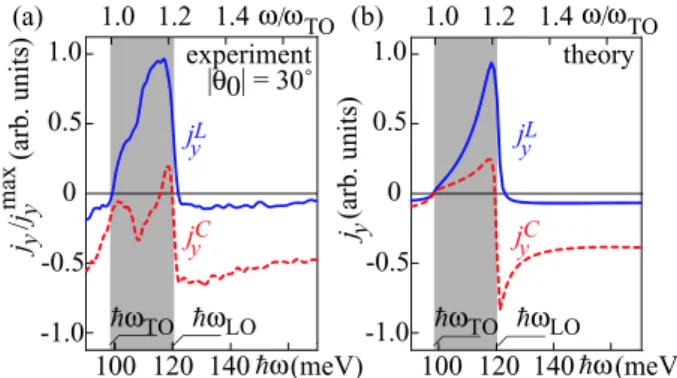
Figure 4. Spectral behaviour of the linear (solid lines) and circular (dashed lines) photocurrents excited by radiation in the frequency range of rest- strahlen band of SiC substrate indicated by a grey background. (a) Exper- imental results. (b) Calculated photocurrents using a ratio of the photon drag to photogalvanic effects equal to−0.3. Data are given after Ref. [14].
PGE closely matches the value obtained by a theoretical estimate for a sufficiently strong degree of asymmetry,V0V1/V02 ≈0.5.
We stress that the PGE requires structure inversion asymmetry, which is not present in graphene where thez→ −zsymmetry is preserved, for example, clean, free standing graphene. As will be detailed in Sec. 6, the observation of the magnetic quantum ratchet effect in epitaxial graphene constitutes a nice example of a large structure inversion asymmetry[19] caused by adatoms or the substrate. Our studies revealed a further interesting feature of photoelectric effects in graphene: A resonance-like frequency dependence for frequencies lying within the reststrahl band of the SiC substrate,[14]seeFigure 4(a). In particular, photocurrents excited by linearly polarized radiation are strongly enhanced just in the range of reststrahlen band, i.e. for frequencies at which the reflection coefficient is close to 100 %. The photocurrent con- sists of photon drag and PGE contributions of similar strength, responding to the in-plane and out-of-plane components of the local electric field felt by the electrons in the graphene layer. The field distribution at a distanced≈2 ˚A from the SiC surface (the position of the graphene layer in our samples, see Ref. [79]) can be calculated using the macroscopic Fresnel formulas. This model describes the observed resonance surprisingly well. The result of the corresponding photocurrent calculations is shown in Figure 4(b). Importantly, those observations demonstrate that by engineering the substrate material and spectral range, we can greatly enhance nonlinear optical and opto-electronic effects in 2D materials.
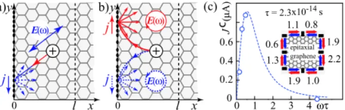
5. Edge Photocurrents
According to the symmetry analysis given in Sec. 2.1 illumi- nation of pristine graphene by radiation at normal incidence does not cause an electric current. When the sample edges are illuminated, however, inversion symmetry is broken, and edge photocurrents can be observed. InFigure 5(a) we illustrate the microscopic process actuating the edge photocurrent. Linearly polarized radiation acts on the free carriers in the semi-infinite graphene plane (x>0). Forωτ <1, the drift motion of the car- riers follows the radiation electric field. In one half of the ra- diation cycle, carriers are moving away from the sample edge.
c
Figure 5. (a) Sketch of the generation of edge photocurrents under illumi- nation by linear polarized radiation (fieldE(ω), blue double arrow). Charge carriers (holes in this case) follow the external field. In one half-cycle of the radiation, they are accelerated towards the sample edge (red arrow), where they are scattered and lose their momentum memory (dashed blue arrows), leading to an edge current jwithin a mean free pathfrom the edge. (b) For circularly polarized radiation, carriers move on circular or- bits, whose sense of rotation depends on the radiation helicity. Similar to (a) they are scattered at the sample edges and generate a net current.
(c) Frequency dependence of the circular component of the edge current showing a maximum atωτ=1. Inset: Magnitude and direction of the cir- cular edge current for opposite helicities (red and blue arrows) showing that the same direction of rotation is maintained along the entire sample boundary. Data are given after Ref. [15].
In the other half cycle, they are accelerated towards the sample edge and eventually scattered by edge roughness, randomizing their momentum. On average, they perform a directed motion which is dependent on the angle between linear polarization and the sample edge, resulting in the linear photogalvanic effect. In a narrow stripe close to the sample edge, up to a distance of roughly the mean free path, an electric current is generated. Un- der circularly polarized radiation, curved trajectories emerge (see Figure 5(b)), as the carriers try to follow the external electric field.
This results in a current reversing its sign, when the radiation helicity changes fromσ+(solid) toσ−(dashed). For fixed helicity irradiation of opposite sample edges also results in the opposite sign of the photocurrent.
Boltzmann kinetic equation for f(p,x,t) describing the edge photocurrents is given by:
∂f
∂t +vx
∂f
∂x+qE(t)∂f
∂p=Q{f}, (14)
where coordinatex≥0 for a semi-infinite layer,qis the carrier charge (q = +|e|for holes and−|e|for electrons), andQ{f}is the collision integral. The distribution function can be expanded in series of powers of the electric field,
f(p,x,t)= f0(εp)+[f1(p,x)e−iωt+c.c.]+ f2(p,x)+ · · · ,(15) where f0(εp) is the equilibrium distribution function, f1∝ |E|, and f2∝ |E|2. The oscillating with frequencyωfirst order in elec- tric fieldE correction f1∝ |E|does not contribute to adccur- rent. Thus, thedccurrent along the structure edge is due to the second orderE-field correction f2and given by
Jy=4q
∞
0
d x
p
f2(p,x)vy. (16)
Here factor 4 takes into account the spin and valley degener- acy. The analysis shows that the total current consists of several
contributions proportional to four Stokes parameters, which all are observed in experiment.
While the edge photocurrents are detected in both epitaxial and in exfoliated samples, in large-area graphene the analysis of the experiments is substantially easier. In exfoliated graphene, opposite edges ofμm-sized flakes are illuminated inevitably. In contrast in large-area samples only a single edge can be illumi- nated. In particular, scanning the laser beam across the sample edges, demonstrated that the coordinate dependence of the signal almost reproduce the Gaussian beam profile. The red and blue ar- rows in the inset in Figure 5(c) illustrate the current directions for σ+andσ−circularly polarized radiation and the numbers show the magnitude of the circular photocurrentJAfor various contact pairs. In these measurements the laser spot is always placed be- tween the contacts at which the signal is picked-up, preventing a temperature gradient between contacts. Remarkably, the edge photocurrent proceeds in the same sense of rotation along the edges of the square shaped samples and changes its direction when reversing fromσ+toσ−polarization.
Edge photocurrents have been detected in a wide range of radi- ation frequencies. Figure 5(c) shows the circular edge photocur- rent JA∝sin 2ϕexcited by THz radiation as a function ofωτ, whereτis the scattering time at a sample edge. The frequency dependency and magnitudes of the circular edge current agrees well with theory. The only parameter used for fit in Figure 5(c) is the scattering time close to the edge, which was found to be quite close to the average bulk scattering time. The small differ- ences can most probably be explained by inhomogeneities in the distribution of scatterers Moreover, the sign of the photocurrent excited at fixed helicity reflects the type of the charge carriers close to the edge. The latter has been shown to be holes even forn-type epitaxial graphene. This is in accordance with scan- ning Raman experiments pointing to ap-type doping at graphene edges,[80,81]transport measurements, where a transition fromn- to p-type at the edges of graphene flakes on SiO2is reported[82]
and growth details of epitaxial graphene.[58,60,83]Thus, edge pho- tocurrents may be used to characterize graphene edge properties up to room temperature.
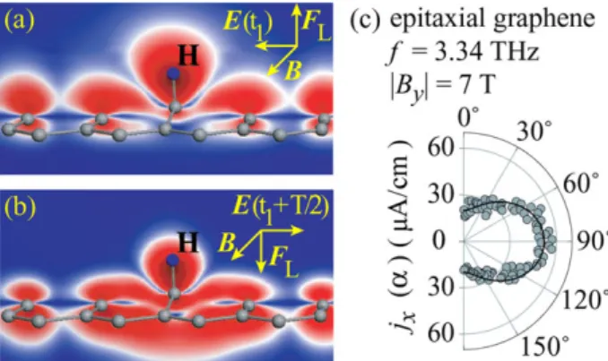
6. Magnetic Quantum Ratchet Effect
The magnetic quantum ratchet effect has been observed in single-layer graphene samples excited with a pulsed molecular terahertz laser and subjected to an in-plane magnetic field. The physics behind the magnetic quantum ratchet effect is illustrated inFigures 6(a) and (b). Dirac electrons are driven by the time- dependent electric fieldE(t) and move in alternating directions in the graphene plane. The external static magnetic fieldBleads to a Lorentz force, deflecting the right-moving electrons upwards and the left-moving electrons downwards (see Figure 6 for an il- lustration at timest1andt2=t1+T/2 differing by a half a period Tof the radiation electric field). For spatially symmetric systems this would lead to a zerodccurrent. However, when, e.g., top ad- sorbates are present, spatial symmetry is broken and electrons shifted above or below the graphene plane experience different degrees of disorder, which results in a non-zerodccurrent. We note that a similar mechanism was discussed for inversion chan- nels in Si and semiconductor quantum wells[78,84,85]and applied to study the inversion asymmetry.[86–88]
Figure 6. (a,b) Electron density distribution in graphene with a hydrogen adatom for two moments in time separated by half a radiation period. (c) Angular dependence of the ratchet current.αdenotes the angle between the external magnetic field and the radiation electric field. Dots: experi- mental data taken atT=115 K,B=7 T and field amplitude of 10 kV/cm.
Solid line: theory. Data are given after Ref. [19].
The current is proportional to the square ofacelectric field am- plitude and the magnetic field strength. Reversing the direction of static magnetic field changes the sign of the photocurrent. It also depends on the angleαbetween theacelectric fieldE(t) and the static magnetic fieldB. A characteristic polarization depen- dence of the magnetic ratchet current is shown in Figure 6(c). The current is maximal for perpendicular electric and magnetic fields and remaining non-zero for parallel fields. The current is well fit- ted by the equation jx= j1cos 2α+j2with two contributionsj1
and j2. Exactly this behaviour follows from the phenomenologi- cal and microscopic theory developed in Ref. [19] and described below.
As an important fact, when comparing two kinds of graphene samples with different surface treatment, we find opposite signs of the slope jx(|By|). While surfaces of samples with graphene encapsulated in a thin polymer film exhibit a positive slope pho- tocurrent, in the sample with unprotected surface the slope is negative, proving differents signs of structure inversion asym- metry (SIA) for both kinds of samples.
We developed a microscopic theory of the observed effect, which agrees with the experiments and is supported by first- principles calculations. The electric current density is calculated using the general expression Eq. (11)
j =4e
p
vf(p,t). (17)
The distribution function can be obtained from the Boltzmann equation
∂f(p,t)
∂t +eE(t)·∂f(p,t)
∂p =Q{f}. (18)
For elastic scattering, it has the form Q{f} = 2π
p
|Vpp|2[f(p,t)− f(p,t)]δ(ε−ε), (19)
where the angular brackets denote impurity ensemble averaging andVppis the matrix element of electron scattering between the
initial and final states with the momenta pand p, respectively.
The ratchet currents originate in the asymmetry of electron scat- tering, which is caused by theσ −π hybridization around the Dirac points in the in-plane magnetic field. Formally, for the mag- netic fieldBy, it is described by the matrix element
Vpp=Vππ−By(px+px) zπσe
επσm0cVπσ, (20)
wherezπσ is the coordinate matrix element between theπ- and σ-band states,επσis the energy distance between the two bands, Vππ andVπσ are the intraband and interband matrix elements of scattering at zero magnetic field,m0is the free electron mass, andcis the speed of light.
After solving the Boltzmann equation, the analysis of the pho- tocurrent as a function of the radiation polarization reveals that the total current consists of several contributions proportional to four Stokes parameter. Individual contributions proportional to the Stokes parameters describing the degree of linear polar- ization and the one given by the radiation helicity describes the linear and circular magnetic quantum ratchet photocurrents. Ex- periments applying radiation with different polarization states demonstrate that all these photocurrents can be excited efficiently in graphene.
Magnetic quantum ratchet effect has also been treated theoret- ically for bi-layer graphene[89]and graphene superimposed by an asymmetric lateral superlattice.[90,91]The former work considered the orbital effect of an in-plane magnetic field on electrons in bi- layer graphene, deriving linear-in-field contributions to the low- energy Hamiltonian arising from the presence of either skew in- terlayer coupling or interlayer potential asymmetry. Estimations revealed that the effect in bi-layer graphene should be by two or- ders of magnitude greater than that in monolayer graphene dis- cussed above. The magnetic ratchet effect is shown to be sensitive to the origin of disorder and to be tunable by gate voltage. A great enhancement of the magnetic ratchet effect is also expected for graphene with asymmetric lateral potential introduced by peri- odic metallic structure on top of graphene,[90,91]see next section.
It has been demonstrated that in this case electric current gener- ation is caused by both radiation-induced heating of carriers and by acceleration in the radiation electric field in the presence of a space-oscillating Lorentz force. The electric currents sensitive to the linear polarization plane orientation as well as to the ra- diation helicity are also calculated. Furthermore, it is shown that in quantized magnetic fields the magnetic ratchet current exhibit 1/B-oscillations resulting from Landau quantization.[91]
7. Terahertz Ratchet Effects in Graphene with a Lateral Superlattice
Ratchet effects discussed in the previous section require a static magnetic field. Another efficient way to generate adcelectric cur- rent caused by ratchet effect implies symmetry reduction due to deposition of a periodic asymmetric lateral metal structure on the top of graphene. This type of graphene ratchets has been ex- perimental realized and systematic study in both (i) epitaxially grown and (ii) exfoliated graphene with an asymmetric lateral pe- riodic potential.[20]The modulated potential has been obtained by
Figure 7. Cross-section (a) and an optical micrograph (b) of the interdig- itated grating-gates: The supercell of the grating gate fingers consists of metal stripes having two different widthsd1=0.5μm andd2=1μm separated by spacingsa1=0.5μm anda2=1μm. This asymmetric su- percell is repeated six times to create a periodic asymmetric potential with periodd=d1+d2+a1+a2=3μm, see panel (b). Data are given after Ref. [20].
fabrication of either a sequence of metal stripes on top of graphene or inter-digitated comb-like dual-grating-gate struc- tures. The latter structure is shown inFigures 7(a) and (b). Our work demonstrated that a polarization dependentdccurrent can be generated by exposing a modulated device to THz laser radi- ation. By applying different voltages to the two gratings, we can control the photocurrent behaviour at different structure asym- metry, carrier type and density. A typical behaviour of the ratchet photocurrents upon variation of back gate potential is shown inFigure 8(a) and (b) for various combination of the top dual- grating-gate potentials. Figure 8(a) shows the data for equipoten- tial top gates as a function of the effective back gate which is de- fined asUBG−U0i, whereUBGis the applied back gate voltage and U0iare back gate voltages of the charge neutrality point measured for the corresponding top gates voltages. It is seen that the signals are strongly enhanced in the vicinity of the Dirac point and have opposite sign for opposite top gate voltages. A substantial signal is also obtained for zero top gate voltage. This signal is due to the electrostatic potential caused by metal film placed in the proxim- ity of graphene. The data presented in Figure 8(b) reveal that the photocurrent reflects the degree of asymmetry induced by differ- ent top gate potentials and even vanishes for a symmetric profile.
The measurements together with a beam scan across the lateral structure prove that the observed photocurrent stems from the ratchet effect.
The experimental data and the theoretical model are discussed by taking the calculated potential profile and near-field effects explicitly into account. The ratchet current consists of the See- beck thermo-ratchet effect as well as the “linear” and “circular”
ratchets, sensitive to the corresponding polarization of the driv- ing electromagnetic force. The results are analyzed in terms of electronic and plasmonic mechanisms of a photocurrent in peri- odic structures. The ratchet photocurrent appears due to the non- centrosymmetry of the periodic graphene structure unit cell. The effect of the grating is twofold: (i) it generates a one-dimensional periodic electrostatic potentialV(x) acting upon the 2D carriers and (ii) it causes a spatial modulation of the THz electric field due to the near field diffraction.[20,92–95]These one-dimensional asymmetries result in the generation of adcelectric current. The ratchet current may flow perpendicular to the metal fingers or along them. The mechanism leading to the photocurrent forma-
Figure 8. (a) Photocurrent jx(α=0) normalized by the radiation power as a function of the relative gate voltageUBG−U0i, whereU0iis defined as the back-gate voltage for which the resistance is the largest at correspond- ingUTG, see panel (a). (b) Gate voltage dependence of the photocurrent jx(α=0),UTG1=UTG2. Insets show carrier density and energy band off- set profiles atUBG= −20 V. Data are given after Ref. [20].
tion can be illustrated on the basis of the photocurrent caused by the Seebeck ratchet effect (thermo-ratchet). This type of ratchet currents can be generated in the direction perpendicular to the metal stripes and corresponds to the polarization independent photocurrent.
The spatially-modulated electric field of the radiation heats the electron gas toT(x)=T¯+δT(x).[96]Here ¯Tis the average elec- tron temperature andδT(x) oscillates along thex-direction with the superlattice period d. In turn, the nonequilibrium correc- tionδT(x) causes an inhomogeneous correction to thedccon- ductivity,δσ(x)∝δT(x). Taking into account the spatially mod- ulated electric field (−1/e)dV/d xwe obtain from Ohm’s law the thermo-ratchet current[95]
jxS= −1 e
dV d xδσ(x)
. (21)
Heree<0 is the electron charge, and angular brackets denote averaging over a spatial period. This photocurrent vanishes if the temperature is spatially uniform, therefore it is called the Seebeck ratchet current.[97]
Besides the thermo-ratchet effect the THz radiation can in- duce additional photocurrents being sensitive to the linear polarization plane orientation or to the helicity of circularly
polarized photoexcitation. These photocurrents have been ob- served in epitaxially grown graphene with lateral superlattice.[20]
Apart from a novel experimental access to the light matter in- teraction in graphene these results may also have an application potential. Photon helicity driven ratchet current can be utilized for a novel kind of all-electric ellipticity meter. So far such de- vices implements circular photogalvanic effect in semiconductor quantum wells.[98,99]Unique nonlinear properties of graphene to- gether with the advantages of ratchet photoresponse[94,100–104]can substantially improve detectors detectivity and time resolution as well as extend the operation spectral range.
To summarize this part, experiments on two different types of graphene structures provided a self-consistent picture demon- strating that the photocurrents (i) are generated due to the pres- ence of asymmetric superlattices, (ii) are characterized by specific polarization dependencies for directions along and across the metal stripes, (iii) change direction upon reversing the in-plane asymmetry of the electrostatic potential as well as changing the carrier type, (iv) are characterized by a complex sign-alternating back gate voltage dependence in the vicinity of the Dirac point, (v) are strongly enhanced around the Dirac point and (vi) have potential for development of the all-electric ellipticity meter.
8. Fast Room Temperature Detectors of THz Radiation
Finally, studying THz radiation induced opto-electronic phenom- ena in graphene is of particular importance not only for for ex- ploring the physical properties of these materials but also for the development of novel THz radiation detectors. In this section we describe an ultrafast bolometric room temperature graphene based THz detector showing 40 picosecond electrical rise time over a spectral range that spans nearly three orders of magni- tude, from the visible to the far-infrared.[23,24]The detector em- ploys a graphene active region with inter-digitated electrodes that are connected to a log-periodic antenna to improve the long- wavelength collection efficiency, seeFigure 9(a), and a silicon car- bide substrate that is transparent throughout the visible regime.
The detector exhibits a noise-equivalent power of approximately 100μW·Hz−1/2 and is characterized at frequencies from 0.6 to 384 THz (wavelengths from 500μm to 780 nm). To estimate the noise-equivalent power a calibrated photon-drag detector was used.[105]
Low frequency measurements have been performed with a pulsed THz CH3F laser operating at a frequency of 0.6 THz.[106]
The laser pulses (about 200 ns duration) are composed of many short peaks (about 1 ns). The repetition rate is 1 Hz and the sig- nals are recorded with a standard digital oscilloscope.
Figure 9(b) shows the graphene detector signal. While the rise time of the detector is less than the pulse duration the detector can be used to analyze the pulse shape. Similar results have been obtained at higher frequencies ranging from 1 to 5 THz by using NH3as laser active medium.
To explore the time resolution of the graphene detector and extend frequency range to higher frequencies measurements at the free-electron laser FELBE (Dresden-Rossendorf) were per- formed. The laser provides a pulse train with a repetition rate of 13 MHz at frequencies between 1.3 and 60 THz. Pulse traces for
Figure 9.(a) Micrograph of the antenna with the graphene flake below the inter-digitated electrodes. Fast response of the detectors at different frequencies obtained with two types of lasers. (b) 0.6 THz , (c) 7.1 THz, (d) 27.8 THz. Data are given after Ref. [24].
frequencies 7.1 and 27.8 THz are shown in Figures 9(c) and (d), respectively. The rise time is mainly limited by the parasitic capac- itance of the antenna and the inductance of the electrical connec- tions. The intrinsic response time of graphene was determined to be about 10 ps using optical autocorrelation measurements.[23,107]
To our knowledge, a similar broad and continuous frequency range of a fast detector was not reported before, and is unique to our device, where graphene as a detector material and SiC sub- strates are combined. Also, we did not find a significant change in detector response when changing the excitation frequency from inside to just outside the reststrahlen band. The pulse trace shown in Figure 9(d) is obtained for frequency f =27.8 THz ly- ing within the reststrahlen band.
Our graphene-based detector enables ultrafast room- temperature detection in a broad frequency range. Given the extremely low heat capacity of charge carriers in graphene, which are heated directly by the incoming radiation, the electron temperature responds strongly. On the other hand, electrons can cool quickly and efficiently via optical phonons.[28] The presented detector is well suited for a great variety of pulsed laser sources like optical-parametric oscillators and amplifiers or difference-frequency mixers, which makes it a very promising device for multicolor ultrafast spectroscopy.
9. Conclusions and Outlook
The physics of nonlinear electron transport and optical phenom- ena in graphene has already resulted in a great variety of fasci- nating effects. We still need to develop a full understanding of many of the effects using new experimental and theoretical con- cepts. For example, tuning the nonlinear response using exter- nal magnetic fields, strain or by combining graphene with other 2D materials will lead to new insights. Moving beyond graphene, similar effects have been already studied in topological insula- tors and applied for their characterization[108–130]and considered