Nuclear Instruments and Methods in Physics Research A 512 (2003) 341–349
First measurements with a frame store PN-CCD X-ray detector
Norbert Meidinger
a,b,*, Stefan Bonerz
a,b, Rouven Eckhardt
a,d,
Jakob Englhauser
a,b, Robert Hartmann
a,d, G unther Hasinger .
b, Peter Holl
a,d, Norbert Krause
a,b, Gerhard Lutz
a,c, Rainer Richter
a,c, Heike Soltau
a,d,
Lothar Str uder .
a,b, Joachim Tr umper .
baMPI Halbleiterlabor, Otto-Hahn-Ring 6, 81739 Munchen, Germany.
bMax-Planck-Institut fur extraterrestrische Physik, Giessenbachstra. Xe, 85741 Garching, Germany
cMax-Planck-Institut fur Physik, F. ohringer Ring 6, 80805 M. unchen, Germany.
dPNSensor GmbH, Romerstrabe 28, 80803 M. unchen, Germany.
Abstract
The PN-CCD camera on the XMM-Newton X-ray astronomy satellite is the most advanced X-ray spectrometer combining high quantum efficiency, high-speed readout and excellent energy resolution. According to the fullframe concept, the whole 6 6 cm
2large CCD-chip area is used as image area, i.e. is sensitive and exposed to X-rays. The camera operates since January 2000 successfully in space without performance degradation. Based on the concept and technology development of the XMM-Newton PN-CCD, the ‘frame store PN-CCD’, a further development of the detector has been proposed. For the new detector a frame store area is added, adjacent to the image area, to allow in parallel photon exposure in the image area and signal readout of the previous image in the frame store area. The concept and the new features of the device will be described here. This comprises in particular a reduced probability of out-of-time event occurrence, the optimization of electronic noise and charge transfer losses as well as a method to obtain a cleaner low-energy response. The first measurements with the new frame store PN-CCD are presented with focus on the above addressed detector parameters. It is planned to apply the device as focal plane instrument for the ROSITA mission that has the aim to extend the ROSAT all-sky survey towards higher energies.
r
2003 Elsevier B.V. All rights reserved.
PACS: 07.85. m; 29.30.Kv; 29.40.Wk
Keywords: Fullframe; Frame store; X-ray spectrometer; PN-CCD; ROSITA; XMM-Newton
1. Introduction
In the previous decade, we had a 6 6 cm
2large PN-CCD developed as focal plane detector for the XMM-Newton X-ray astronomy mission of the European space agency ESA. It detects single X-ray photons from cosmic sources that are
*Corresponding author. Max-Planck-Institut fur extraterres-. trische Physik, GiessenbachstraXe, 85741 Garching, Germany.
Tel.: +49-89-839400-22; fax: +49-89-839400-11.
E-mail address:nom@mpe.mpg.de (N. Meidinger).
0168-9002/03/$ - see front matterr2003 Elsevier B.V. All rights reserved.
doi:10.1016/S0168-9002(03)01912-0
imaged by a Wolter-I-type telescope to the focal plane CCD-detector. The photon’s X-ray energy is measured in the energy band from 0.1 up to 15 keV as well as its position and time of incidence on the detector.
The main characteristics of the PN-CCD detector performance are the high quantum efficiency, e.g. about 90% at an energy of 10 keV, and the ultra-fast readout, which allows for a frame rate of 14 images per second in the fullframe mode [1]. The energy resolution is close to the theoretical Fano noise limit for X-ray energies above 1 keV. For example, the FWHM of the Mn-Ka line at 5894 eV amounts to 155 eV for the PN-CCD camera aboard XMM-Newton. The pixel size was matched to the angular resolution of the telescope and for this reason a relatively large format of 150 150 mm
2was realized.
The XMM-Newton satellite was launched in December 1999. Since first commissioning in space in January 2000, the PN-CCD camera operates without degradation of energy resolution. This is in agreement with the expected high radiation hardness of the backside illuminated PN-CCD.
Only the impact of a micrometeoroid on the photon entrance window during revolution x156 had produced several bright pixels [2].
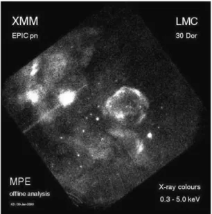
In spite of the successful PN-CCD camera in orbit, there is potential for further detector improvement. An example is the probability of out-of-time (OOT) event occurrence. A photon shows up as OOT event if it hits the CCD during the transfer of the image to the anodes and not during integration time. The consequential corrup- tion of position information of OOT events in transfer direction results in a slight smearing of the image over the whole transfer channel. A look at the ‘first light’ image of the PN-CCD camera in orbit, which is shown in Fig. 1, illustrates the effect of out-of-time events. Several suggestions for PN- CCD improvement concerning noise, charge transfer efficiency (CTE) and low-energy response resulted in the development of a new device, called
‘frame store PN-CCD’ (FS PN-CCD).
An application for this novel PN-CCD type will be the ROSITA project [3,4]. ROSITA which means ROentgen Survey with an Imaging Tele- scope Array, extends the all-sky survey of ROSAT
(0.1–2.4 keV) [5] to higher energies up to 12 keV and achieves a better energy resolution. It is planned to accommodate ROSITA on the Inter- national Space Station (ISS). Each of the seven Wolter I-type telescopes focuses the X-rays on the image area of a dedicated FS PN-CCD detector.
As minimum frame rate are 20 images per second required. Otherwise, the position resolution would be substantially lowered due to the scan motion of ROSITA. The thermal budget allows on the other hand no considerably higher frame rate due to the increase in power dissipation.
2. Concept of the frame store PN-CCD
The concept of the FS PN-CCD is based on that of the PN-CCD [1]. The device is fully depleted by reverse biased voltages applied to PN-junctions on the front and backside of the CCD, i.e. to the transfer registers and to the photon entrance window (see Fig. 2). By the choice of appropriate
ARTICLE IN PRESS
Fig. 1. ‘First light’ image of the PN-CCD camera on the XMM-Newton satellite. It shows a part of the 30 Doradus Nebula in the Large Magellanic Cloud (LMC) observed with the 66 cm2large detector, which is subdivided into an array of 26 CCD units. On the left a slight smearing of the brightest X-ray source, the N157B, along the transfer channels is clearly visible. It is caused by out-of-time events whose ratio is 6% of all detected photons in fullframe mode.
N. Meidinger et al. / Nuclear Instruments and Methods in Physics Research A 512 (2003) 341–349 342
voltage values, a potential shape is created in the n-type silicon with maximum in a depth of about 7 mm. Incoming X-rays enter the image area of the CCD from the backside through a large area thin p-implanted layer, called back contact. The electron–hole pairs, generated by the X-ray photon, are separated due to the electric field.
The electrons drift to the potential maximum that is located inside a layer of low resistivity (approxi- mately 40 O cm) on top of the bulk material with high resistivity (2–5 kO cm). During photon inte- gration time, the signals are stored in the potential wells of the pixels built-up by three transfer registers with two different voltage levels applied.
Then the signals are transferred with high speed from the image to the frame store section that is shielded against X-rays. The frame store concept is already known from X-ray MOS-CCDs. For this
CCD-type it is necessary due to the long readout time of the image. The frame store comprises the same number of pixels as the image section but of smaller format in order to save device area. While X-ray photons are accumulated in the image area for a new picture, the previous image in the frame store is read out row by row. As already realized in the PN-CCD, each transfer channel is terminated with an anode. Thus, no serial charge transfer like in other spectroscopic CCDs is necessary. The anode again, is connected to the gate of a JFET, called ‘first FET’, which is monolithically imple- mented on the CCD-chip (on-chip electronics).
Wire bonds connect the source of the JFET with a dedicated preamplifier channel.
Thus, charge transfer as well as signal readout is performed simultaneously for all channels. The signals of the next row are read in, while the data
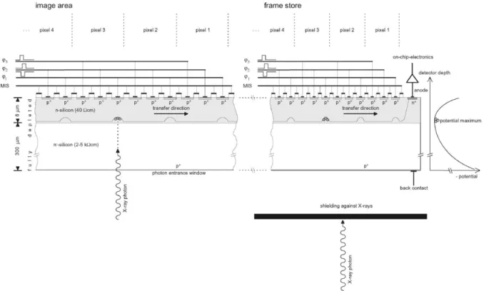
Fig. 2. The schematic diagram shows a cross-section through a frame store PN-CCD along a transfer channel and to the right, the shape of the electric potential in the device vs. depth. The device thickness of about 300mm is fully depleted by reverse biased diodes on the front and backside of the CCD. The X-rays enter the CCD from the backside. The frame store area is shielded against X-rays. The generated signal electrons are collected and transferred in a depth of about 7mm inside a layer of relatively low resistivity. Each FS PN- CCD channel comprises the pixels of the image area, the pixels of the frame store area (same number but of smaller format) and an anode connected with the gate of an on-chip JFET for signal amplification.
of the previous row are multiplexed to the output line of the preamplifier chip. By this method, a high-speed readout is achieved.
The radiation hardness of the PN-CCD is also valid for the FS PN-CCD because the concept concerning radiation hardness and the fabrication technology are the same (for details see Ref. [6]).
In particular, the self-shielding of the backside illuminated PN-CCD by the device thickness is important for detector applications in space because Wolter telescopes focus protons with energies up to more than hundred keV onto the focal plane detector [7]. As the critical charge transfer depth is far-off the radiation entrance window of the detector, separated by a distance of almost 300 mm, even protons with an energy of 5 MeV do not reach the transfer channel.
The fact that the transfer registers and the photon entrance window of the PN-CCD are realized by PN-diodes, explains the device’s name, whereas all other CCDs use MOS-gates for the charge transfer. Since the frame store is the most obvious feature of the improved PN-CCD type, the device is called frame store PN-CCD to distinguish it from the PN-CCD of XMM-Newton.
3. First measurements and performance characteristics
The methods, used for the FS PN-CCD to improve the performance characteristics of the PN-CCD, are described in this section. The first measurement results with FS PN-CCDs demon- strate the benefit of the device development.
3.1. Out-of-time events
The probability that a photon appears as out-of- time event is given by the ratio of the transfer time in the image area to the total exposure time. The latter is defined by the sum of integration time and transfer time.
In the case of the PN-CCD without frame store all pixels of the detector belong to the image area and are thus exposed to X-rays. For redundancy reasons the 6 6 cm
2large flight PN-CCD is
divided into an array of 2 6 independent subsystems, each comprising 64 transfer channels and 200 rows. After the transfer of the image by one row, the signal charges on the anodes are amplified and processed. While the same operation is carried out for the next row, the signals of the previous row are read out to the ADC. The transfer is performed fast (within less than a ms) but the low-noise signal processing and the multi- plexing of 64 preamplifier channels to the single output channel respectively, is time consuming.
The transfer and readout of one row takes 23 ms and 4.6 ms for the entire CCD-subsystem with 200 rows. The PN-CCD is exposed to X-rays during the whole cycle time that is 73 ms in the standard fullframe mode. Thus the probability of out-of- time events amounts to 4.6 ms/73 ms=6.3%.
The FS PN-CCD allows for a fast transfer of the complete image into the frame store. The slow read out, row by row, is then performed without suffering from more out-of-time events since the frame store area is shielded against X-rays.
The advantage of the frame store mode con- cerning OOT events has been demonstrated in an experiment. A recently fabricated FS PN-CCD prototype was operated once in full frame mode and another time in the frame store mode. In full frame mode the whole device area, i.e. all 250 rows, were exposed to X-rays. In frame store mode, only 125 rows of the CCD were used for imaging whereas the other 125 rows served as frame store and were shielded for that purpose.
The pixel format in the image area is 75 75 mm
2and it is 75 51 mm
2in the frame store section.
The frame rate has been chosen in both modes to 20 images per second, as planned for the ROSITA mission. A mask with three pinholes was mounted in front of the CCD so that out-of-time events could be easily recognized by their location outside the illuminated spots on the detector. The CCD was exposed to the same photon flux in both operating modes (see Fig. 3). In full frame mode the transfer including the readout of the 250 rows lasted 7.0 ms yielding an out-of-time event prob- ability of 14%. Using the new operating mode, the fast transfer of the image (125 rows) into the frame store could be carried out within 175 ms, resulting in 0.35% out-of-time events. The comparison
ARTICLE IN PRESS
N. Meidinger et al. / Nuclear Instruments and Methods in Physics Research A 512 (2003) 341–349 344
shows that the occurrence of out-of-time events was reduced by a factor 40 in this experiment when the CCD was operated in frame store mode (with a reduction in image area by a factor of two).
For the test, we had not yet optimized the transfer speed. In former experiments with PN- CCDs operated in fast modes, a transfer time shorter by a factor of three had already been achieved. This means again a factor of 3 less out- of-time events in frame store mode operation or 0.12% in total for the example above.
3.2. Electronic noise
The electronic noise determines together with the dark current noise, the Fano noise, the transfer noise, and the noise contribution associated with partial and split events, the energy resolution of a spectroscopic CCD detector. In particular, for low X-ray energies E
xwhere the Fano noise contribu- tion is small since it increases with E
1=2x[8], the electronic noise is one of the main noise contribu- tions. For the FS PN-CCD, the electronic noise was improved in consequence of a reduction in readout capacitance from 120 to 50 fF. This was mainly achieved by the waiving of the reset FET, which is part of the on-chip electronics and of same type as the first FET. The function of the reset FET is to clear the charge on the anode by an appropriate voltage pulse applied to the gate. For the FS PN- CCD an alternative way of charge reset was chosen.
It is a continuous clear mode by means of the gate to drain current of the First FET, which is operated in source follower configuration [9]. The ‘weak’
avalanche breakdown mechanism which occurs between gate and drain in the transistor channel, is self-regulating in dependence on the current to the anode. By application of this clear mechanism, the capacitance arising from the reset FET and its feed lines could be saved.
The measurement of the electronic noise of the FS PN-CCD yielded a value of 3.5 electrons equivalent noise charge (ENC). The improvement is evident by a comparison with the PN-CCD of XMM-Newton where an electronic noise of 5 electrons was achieved.
3.3. Charge transfer inefficiency
After the end of integration time, the signal electrons stored in the pixels are transferred along the channels to the anodes. The transfer causes signal charge losses due to the capture of single electrons in traps within the silicon lattice. The charge transfer inefficiency (CTI) characterizes the charge loss per pixel transfer in relation to the signal charge. The CTE is the complement to CTI, i.e. CTE=1 CTI. The signal transfer losses cause a noise contribution, called transfer noise, which increases with the number of lost electrons.
Fig. 3. Operation of a FS PN-CCD in fullframe mode (left figure) and in frame store mode with 125 rows for the image area and the other 125 rows as frame store (right figure). A mask with three different pinhole sizes was mounted in front of the detector. The same frame rate (20 images/s) and the same Al-K X-ray flux was used for both measurements. The out-of- time events appear outside the illuminated spots distributed all over the transfer channels. The fast transfer of the image into the frame store (frame store mode) instead of transfer and read out row by row as performed in the fullframe mode, reduces the out-of-time event occurrence by a factor of 40 to a value of 0.35%.
The CTI of the PN-CCD is for typically applied temperatures of 90
C mainly determined by titanium traps, which are present in the silicon with a concentration in the order of 10
10cm
3. The origin of the titanium impurity was due to the epitaxy process [10].
Another method to provide a layer of relatively low resistivity for signal charge storage and transfer, avoiding the epitaxy process, is a high- energy implantation of phosphorus atoms. The doping profile is extended to a depth of about 8 mm according to the maximum penetration depth of 20 MeV phosphorus ions in silicon.
The CTI measured for the new FS PN-CCDs with high-energy implant, gave a value of 5 10
5for Al-K X-rays (1486 eV) at a temperature of 90
C. With the PN-CCD on XMM-Newton, a CTI value of 6.6 10
4was determined for the same X-ray energy and temperature. The compar- ison shows that an improvement in charge transfer losses by a factor of about 13 was achieved with the FS PN-CCD (see Fig. 4).
3.4. Energy resolution
The decrease in CTI and consequently transfer noise, improves together with the reduction of electronic noise, the energy resolution of the spectro- scopic detector. For the analysis, the FS PN-CCD was exposed to a flat field illumination with Al-K X- rays. Fig. 5 shows the spectrum of the Al-K line. The full-width at half-maximum (FWHM) of the line gives a value of 76 eV. The result of the measure- ments with the PN-CCD flight camera yielded a FWHM of about 110 eV for the same X-ray line.
3.5. Low-energy response
If electronic and transfer noise contributions are already small, a high charge collection efficiency is the most critical point, to achieve a good low- energy response for the CCD. This is because the penetration depth of low-energy photons is rela- tively small but close to the photon entrance window the density of traps is relatively high and the electric drift field is weak.
A substantial improvement of the charge collection efficiency was obtained by the choice
of / 1 0 0 S silicon instead of / 1 1 1 S silicon which has been used for the XMM PN-CCD.
The benefit of / 1 0 0 S silicon is a lower density of traps at the Si–SiO
2interface. A detailed description of early measurements and modeling, analyzing the different low-energy response of / 1 1 1 S and / 1 0 0 S silicon is given in [11]. Fig. 6 shows the spectrum of the C-K line (277 eV) for which the 1/e absorption length (i.e. attenuation length) in silicon is about 120 nm. The FWHM
ARTICLE IN PRESS
Fig. 4. The scatter plot shows the signal amplitudes of Al-K X- rays (1486 eV) in dependence on the number of pixel transfers to the anode for a FS PN-CCD. The measured CTI of 510 5 is equal to a drop of the signal amplitudes for about 1.2% after 250 pixel transfers. The corresponding decline of the Al-K signal amplitudes of the PN-CCD on XMM-Newton is plotted for comparison. The FS PN-CCD has been operated here in fullframe mode for conformance reasons with the PN-CCD and the frame store area was not shielded. The above-described larger pixel format in the image area (row 126–250) than in the frame store explains the evidently higher number of photons collected in the image area.
N. Meidinger et al. / Nuclear Instruments and Methods in Physics Research A 512 (2003) 341–349 346
of the line amounts to 82 eV; the ‘peak to background’ ratio is 25.
Nevertheless, the charge collection of the generated signal electrons is still incomplete resulting in a broadening of the signal peak and a shift of about 40 eV towards lower energies.
However, it is a substantial improvement com- pared to the XMM PN-CCD because the C-K line is now clearly separated from the noise peak and appears with an approximately Gaussian shape.
For a further improvement regarding the shift of the peak position and the energy resolution, the drift field at the PN-junction of the entrance window has to be increased. This is accomplished by the implantation of boron atoms through a
SiO
2-layer to obtain a shallower doping profile and by an additional phosphorus implant. First test results of the method are described in Ref.
[11]. The thereby enhanced electric field at the photon entrance window reduces the probabilities for recombination of generated electron–hole pairs and for trapping of signal electrons because of the increase in the drift velocity of the charge carriers.
3.6. Split events
After the generation of the signal electrons by an X-ray photon, they drift to the potential max- imum. During the drift time, the charge carriers disperse due to diffusion and mutual electrostatic
Number of Events
Energy (keV)
0 0.5 1 1.5 2 2.5
0 500 1000 1500 2000 2500 3000 3500 4000 4500 5000 5500 6000
Fig. 5. Spectrum of the Al-K line (single events only) measured with a FS PN-CCD. All pixels of the 250 rows have been illuminated with X-rays in this flat field measurement. The analysis of the energy resolution gives a FWHM of 76 eV for the line after correction of the charge transfer losses, which has been carried out as usual.
Fig. 6. Low-energy response of the present FS PN-CCDs measured with the C-K line (277 eV). The line is clearly separated from the noise peak and its FWHM was determined to 82 eV. The shift of the peak position for about 40 eV to a lower energy indicates a still incomplete charge collection. An optimized implantation profile of the photon entrance window PN-diode will further reduce the peak shift and improve the FWHM.
repulsion. Finally, the signal electrons either are collected in a single pixel or spread over up to four pixels in dependence of the position of the X-ray photon relative to the pixel border. The terms for the different signal patterns are single and split events, respectively. The benefit of split events is the improvement of position resolution, which is then no more determined only by the pixel size.
However, there is a disadvantageous effect regard- ing the energy resolution because the electronic noise increases with the number ‘n’ of the involved pixels by a factor of n
1=2:
The smaller pixel size of the FS PN-CCD (75 75 mm
2) in comparison to that of the XMM PN-CCD (150 150 mm
2) causes a higher prob- ability for event splitting. The difference in numbers is exemplified by measurements with Al- K X-rays and an event detection threshold set to 100 eV (chosen to allow a comparison with the PN-CCD of XMM):
Pixel size: (75 mm)
2(150 mm)
2Single events: 57% 70%
Double events: 38% 28%
Triple events: 3.0% 1.6%
Quadruple events: 2.0% 0.4%
The probabilities may vary a little for different operating voltages of the devices, but single events are the most frequent pattern type for both pixel sizes. However, for the smaller pixel size of 75 75 mm
2, more than 40% of the events appear as split events. Their ratio increases when a lower event detection threshold is applied.
4. Further development of frame store PN-CCDs Presently we fabricate FS PN-CCDs with a pixel size of 50 51 mm
2. The increase in split event probability of these devices is important for applications with higher requirements for position resolution.
Up to now, wafers with a diameter of 4 inches and a thickness of about 300 mm have been used for device fabrication in the MPI Halbleiterlabor.
In the near future, we will process wafers of six inches diameter providing a thickness of about
500 mm. Since the wafer thickness is according to the device concept almost equal to the depletion depth, it determines the quantum efficiency for high-energy X-ray photons which have large absorption lengths. As a result, the quantum efficiency is higher for the new devices, e.g. it rises for 10 keV photons from 90% to 98%, and for 15 keV X-ray energy we find 67% instead of 49%. The increase of device thickness causes furthermore a longer drift time of the signal electrons and thus more signal spreading. Conse- quently, the ratio of split events to single events becomes higher.
The times for fast transfer and for readout of the rows were chosen relatively conservative in the first performance tests. After optimization of transfer and readout times, the probability of out-of-time event occurrence will be further minimized as well as the charge transfer losses by traps. The latter is a consequence of the reduced potential capture time for electrons during the transfer.
5. Summary and outlook
The first measurements with frame store PN- CCDs showed very encouraging results. The device can be operated either in frame store mode or it runs in full frame mode, like the PN-CCD for XMM-Newton using then all pixels for imaging.
The benefit of the frame store mode is the minimization of out-of-time event occurrence by a fast transfer of the image into the shielded frame store area. The improved energy resolution of the CCD is demonstrated by a FWHM of 76 eV for the Al-K line at 1486 eV. This was achieved by a low electronic noise of 3.5 electrons and a CTI of 5 10
5. The low-energy response is demonstrated by the C-K spectrum (277 eV) showing a FWHM of 82 eV and a peak to background ratio of 25. The performance parameters of the FS PN-CCD show essential improvements compared with the PN-CCD on XMM-Newton. Methods have been presented for a further improvement of detector performance.
The pixel size of the first devices was chosen to 75 75 mm
2in the image area as required by the
ARTICLE IN PRESS
N. Meidinger et al. / Nuclear Instruments and Methods in Physics Research A 512 (2003) 341–349 348
main project for the development of FS PN- CCDs, the German ROSITA X-ray astronomy mission. It is a follow-up mission of the ROSAT all-sky survey.
Another possible field of application for the FS PN-CCD could be ‘adaptive optics’. A wave front sensor needs a smaller pixel size of about 50 50 mm
2as well as a higher frame rate.
Approximately 1000 images per second are likely attainable with the multi-parallel readout archi- tecture of the detector.
Finally, the FS PN-CCD has the capability to fulfill the demands on the wide field imager for the XEUS project, ESA’s future X-ray astronomy project after XMM-Newton.
Acknowledgements
The authors would like to thank all people contributing to this paper, in particular the colleagues of the MPI Halbleiterlabor for the fabrication and mounting of the devices.
The project was supported by the Heidenhain foundation.
References
[1] L. Struder, et al., Astron. Astrophys. 365 (1) (2001). L18.
[2] L. Struder, et al., PN-CCDs on XMM-Newton-30 Months. in Orbit, Nucl. Instr. and Meth. A, these Proceedings.
[3] P. Predehl, Proc. SPIE 4851 (2003) 314.
[4] N. Meidinger, et al., Proc. SPIE 4851 (2003) 1040.
[5] W. Voges, et al., Astron. Astrophys. 349 (1999) 389.
[6] N. Meidinger, B. Schmalhofer, L. Struder, Nucl. Instr. and. Meth. A 439 (2000) 319.
[7] L. Struder, et al., Proc. SPIE 4012 (2000) 342..
[8] P. Lechner, L. Struder, Nucl. Instr. and Meth. A 354. (1995) 464.
[9] C. Fiorini, P. Lechner, IEEE Trans. Nucl. Sci. NS-46 (3) (1999) 761.
[10] N. Krause, H. Soltau, D. Hauff, J. Kemmer, D. Stotter,. L. Struder, J. Weber, Nucl. Instr. and Meth. A 439 (2000). 228.
[11] R. Hartmann, D. Hauff, P. Lechner, R. Richter, L. Struder, J. Kemmer, S. Krisch, F. Scholze, G. Ulm,. Nucl. Instr. and Meth. A 377 (1996) 191.