Frame Store PN-CCD Detector for Space Applications
Norbert Meidinger* a , Ladislav Andricek b , Stefan Bonerz a , Jakob Englhauser a , Robert Hartmann c , Günther Hasinger a , Sven Herrmann a , Peter Holl c , Rainer Richter b , Heike Soltau c , Lothar Strüder a
a Max-Planck-Institut für extraterrestrische Physik, Giessenbachstrasse, 85741 Garching, Germany
b Max-Planck-Institut für Physik, Föhringer Ring 6, 80805 München, Germany
c PNSensor GmbH, Römerstrasse 28, 80803 München, Germany
ABSTRACT
The fully depleted PN-CCD detector is meanwhile field-tested in several experiments on ground and in space. Its application as focal plane detector aboard ESA’s XMM-Newton observatory can be considered as the most impressive one. The further development of this detector type including its readout chip in the MPI semiconductor laboratory is presented here. The new device, called frame store PN-CCD, shows substantial improvement of performance, in particular concerning the energy resolution and the probability of out of time event occurrence. Moreover, the detector offers features which are of great importance for its application in space. This is, besides the radiation hardness of the CCD, the variety of feasible pixel sizes and the high frame rates in combination with the small power consumption of the detector. Because of the thin radiation entrance window and the full depletion of the chip, the detector provides a high quantum efficiency for soft X-rays as well as for optical light and the near infrared. The frame store PN-CCD detector will be applied for the proposed X-ray astronomy missions DUO and ROSITA.
Keywords: DUO, frame store, PN-CCD, ROSITA, XEUS, XMM-Newton, X-ray detector.
1. INTRODUCTION
The PN-CCD is one of three focal plane detectors aboard ESA’s XMM-Newton satellite
1. After launch of the observatory in 1999 with an ARIANE V, the PN-CCD detector operates in the meantime successfully for more than 3.5 years. The same detector type was also employed for the German ABRIXAS mission
2. However, the satellite failed immediately after launch in 1999 because of a defect in the main power supply system. On ground, the PN-CCD detector is applied in numerous experiments, for example in multi-photon
3and transition radiation
4experiments, in X-ray microscopy
5and in channeling
6experiments as well as for the search of axions
7, theoretically predicted elusive particles.
The further development of the PN-CCD and its dedicated CAMEX readout chip is presented in the next sections. They are the main components of the focal plane detectors for the planned X-ray astronomy missions DUO, a NASA satellite, and ROSITA
8,9,10, a German experiment accommodated on the International Space Station. For ESA’s next great X-ray astronomy mission XEUS
11, the frame store PN-CCD could be the right choice too, as the detector has the capability to meet all the requirements for the wide field imager (WFI). This includes the demanded high frame rate of 10
2– 10
3per second for an image area of approximately 60 cm
2.
2. DETECTOR CONCEPT
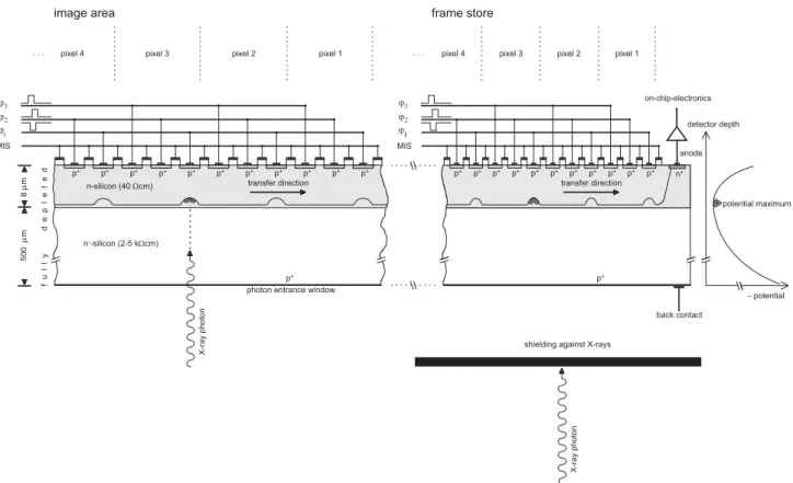
The PN-CCD is structured by pn-diodes in contrast to other charge coupled devices
12. This applies in particular to the transfer registers of the pixels, the photon entrance window and the first stage of signal amplification on the CCD chip (see Figure 1). A fill factor of 100 % is achieved for the image area. The chip thickness of 300 P inch wafer) and 500 PLQFKZDIHUUHVSHFWLYHO\LVIXOO\GHSOHWHGLHVHQVLWLYHWRLRQL]LQJUDGLDWLRQ The photon or particle radiation enters the device from the backside through a large area homogeneous boron implant of ultra-shallow depth. By means
* nom@hll.mpg.de
of reverse biased diodes on both chip surfaces, a potential maximum is created deep in the silicon. Thus storage and transfer of the generated signal electrons is accomplished in a depth of about 7 PZLWKLQDOD\HU which shows about two orders of magnitude lower resistivity than the ultra-pure n-doped substrate. The layer is meanwhile manufactured by a high-energy (20 MeV) implant of phosphorus, while for the XMM PN-CCD it was epitaxially grown. As a result of the high-energy implant method the impurity concentration in the transfer depth was minimized, and we achieved a substantial improvement in charge transfer efficiency
14. The depth of the charge transfer allows for a large variety of feasible pixel sizes. To date, devices with pixel sizes between 50 PDQG PKDYHEHHQIDEULFDWHG The signals are amplified by a JFET which is monolithically integrated on the CCD chip at the end of each transfer channel. The source of the transistor is connected by a wire bond with the input stage of the multi-channel CAMEX readout chip, an ASIC fabricated with a JFET-CMOS process. Signal processing is performed in the CAMEX chip simultaneously for all pixels of a CCD row, i.e. 2 x 128 pixels in the case of a DUO and ROSITA detector (Figure 2). The parallel architecture of the detector system for charge transfer, on-chip signal amplification and signal readout, permits very short readout times of the images.
on-chip-electronics detector depth
- potential potential maximum
500 µm 8µm
n--silicon (2-5 kΩcm)
anode
transfer direction ϕ
ϕ2 ϕ3
1 MIS
p+ p+ p+ p+ p+ p+ p+ p+ p+ p+ p+ n+
photon entrance window
p+
back contact
f u l l y d e p l e t e d
pixel 1 pixel 2
pixel 3 pixel 4
. . .
X-ray photon
p+ p+ p+ p+ p+ p+ p+ p+ p+ p+ p+
p+ pixel 1 pixel 2
pixel 3 pixel 4
. . .
transfer direction ϕ
ϕ2 ϕ3
1 1
MIS
image area frame store
shielding against X-rays
X-ray photon
n-silicon (40 Ωcm)
Figure 1: Schematic cross section through a frame store PN-CCD along a transfer channel (left hand) and shape of the electric potential vs. depth (right hand). The device is depleted over its full thickness of 300 PR r 500 PE\UHYHUVHELDVHGGLRGHVRQWKH front side and backside of the CCD. X-rays enter the image area from the backside of the CCD. The generated electrons are stored and transferred in a depth of about 7 PEHORZWKHIURQWVLGHZLWKLQDUHJLRQRI higher dopant concentration than in the substrate. Each individual channel is terminated by an anode. The anode is connected with the gate of a JFET which is integrated on the chip for signal amplification. The source is again connected with the input of the dedicated CAMEX channel.
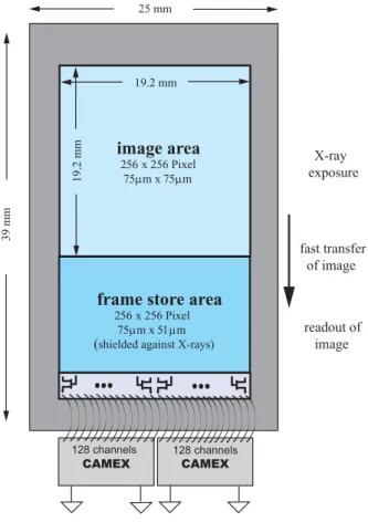
The fast readout allows for the choice to operate the imaging detector in frame store mode or in fullframe mode without
crucial drawbacks. In frame store operation the readout section is shielded against X-rays. In this mode we achieve a
smaller probability for out of time (OOT) event occurrence. Only the fraction of X-rays which hit the image area during
the fast transfer (which lasts 75 V IRU WKH '82 ROSITA detector with 256 rows), suffers a corruption in position
information regarding the transfer direction. Thus about 0.15 % of the X-ray photons will be affected in the case of DUO and ROSITA. An alternative operational mode is to extend the image area over all pixels of the CCD. The larger image area which is obtained in fullframe mode has the disadvantage to suffer for more out of time events. Their ratio is given by the readout time and the cycle time. The PN-CCD detector aboard XMM is for example operated in fullframe mode. The OOT fraction amounts to 6 % in fullframe mode. Without fast readout the imaging would be strongly affected in fullframe mode due to the high fraction of OOT events or alternatively, the time resolution of the CCD would be low because of a necessarily long cycle time to reduce the OOT event fraction.
image area
256 x 256 Pixel 75µm x 75µm
frame store area
256 x 256 Pixel 75µm x 51µm
25 mm
39 mm
X-ray exposure
fast transfer of image
readout of image (
shielded against X-rays)19.2 mm
19.2 mm
CAMEX CAMEX
128 channels 128 channels
Figure 2: Schematics of the frame store PN-CCD detector for the DUO and the ROSITA project. The X-rays are focused by a Wolter telescope onto the image area comprising 256 x 256 pixels. After 50 ms exposure time the image is transferred to the frame store section within 75 V . Then, the signals are amplified on the chip and read out row by row. This is accomplished by the use of 256 anodes assigned to 256 JFETs on the CCD. The transistors are again connected by wire bonds with two CAMEX chips providing 128 channels each. After amplification and filtering of the 128 signals in parallel, they are stored to be multiplexed to both or to only one of the CAMEX output nodes. In the case of DUO and ROSITA where no extreme fast readout is required, only one node per CAMEX is used to limit the number of ADCs. The readout of an image takes a time of about 5 ms.
3. DETECTOR CHARACTERISTICS
3.1 Key parameters
The frame store PN-CCD detector has been developed and fabricated in the MPI semiconductor laboratory. The main
performance parameters of the new CCD detector are summarized below. They are completed by most recent
measurement results about charge handling capability, operation with minimum clock voltage amplitudes, and chip
surface passivation.
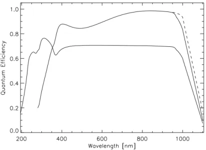
The quantum efficiency for X-rays is in the whole energy band from 0.3 keV to 12 keV at least 90 % for the 500 P thick PN-CCD
10. In the domain of visible light and near infrared a similar high quantum efficiency is obtained (see Figure 3).
Figure 3: Quantum efficiency of the PN-CCD for optical and near infrared light calculated for two different antireflective coating layers. The layers consist of different SiO
2and Si
3N
4layers to enhance the response to “red” and near infrared respectively to “blue”
light. The dashed line shows the quantum efficiency for a wafer thickness of 500 P ZKLOH WKH VROLG OLQHV DSSO\ IRU P thickness
13.
With the revised on-chip electronics of the frame store PN-CCD an electronic noise figure of 3.5 electrons rms is achieved
14. In single photon counting mode we measure an energy resolution of 76 eV FWHM for the Al-K line (1486 eV) generated by an X-ray tube. The quality of the photon entrance window is demonstrated by the excellent response at low energies which shows a FWHM value of 82 eV for the C-K line (277 eV).
The time resolution of the CCD is limited by the minimum readout time for the image. A signal processing time of at most 20 VSHU row (128 pixels) results in a readout frequency of more than 6 Mpixel/s. The ROSITA CCD is read out by two CAMEX128 chips in parallel which yields a readout time of 5 ms for the 3.7 cm
2large image area. The decision to operate the detector with a longer cycle time of 50 ms and thus less heat dissipation, originates from the small thermal budget in space for the cooled focal plane detector.
The outstanding radiation hardness and long term stability of the detector is evident by the experiences gathered with the PN-CCD detector aboard the XMM-Newton satellite
15. This is mainly due to the fact of self-shielding of the thick backside illuminated device, the fast readout, and the deep transfer.
For applications in X-ray astronomy a spectroscopic detector has to be shielded against visual light to achieve highest energy resolution. For the PN-CCD this can be realized on chip by a deposition of a thin and homogeneous aluminum layer (e.g. 50 nm or 100 nm) on the photon entrance window
10. The experience to accomplish such thin layers with homogeneous thickness is gained from the fabrication of silicon drift detectors (SDD) in our laboratory.
3.2 Charge handling capability
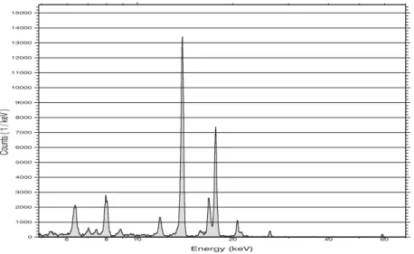
A spectroscopic (i.e. open) Am
241source HPLWV -particles in a small energy band from 5.4 MeV to 5.5 MeV. Due to
their short range in silicon of less than 30 PWKHLUHQ ergy is completely absorbed in the PN-CCD. In addition WRWKH -
particles, lower energetic X-rays and gamma rays are emitted in consequence of the radioactive decay process of the
Am
241isotope (see Table 1). The most energetic line (with significant emission probability) appears at 60 keV.
-particles X- -rays Energy Emission
probability Energy Emission probability
5.388 MeV 1.4 % 11.9 keV 0.8 %
5.443 MeV 12.8 % 13.9 keV 13.0 %
5.486 MeV 85.2 % 17.6 keV 20.2 %
21.0 keV 5.2 % 26.3 keV 2.4 % 59.5 keV 35.7 %
Table 1: Energies of alpha particles and most important photon lines which are emitted from an Am
241source
16. The associated emission probabilities are presented as well.
For an estimation of the charge handling capability of the PN-CCD we exposed the detector to an Am
241source. The CAMEX64B ASIC was operated in low gain mode for these measurements. Thereby, signal energies up to about 300 keV can be resolved. Figure 4 shows the spectrum of the Am
241source measured with a PN-CCD detector. The - SDUWLFOHVFDQEHHDVLO\GLVFULPLQDWHGIURPWKHSKRWRQVE\WKHLUHQHUJ\$QDQDO\VLVRIWKH -particle events revealed that their generated signal electrons are spread over four or more pixels 7KHGLYHUVHHYHQWSDWWHUQVRIWKH -particles (see Figure 5) result from their different positions of incidence referring to the pixel borders and the relatively large size of the charge clouds after drift to the potential maximum. The size of the charge cloud is caused by the diffusion and mutual electrostatic repulsion of the signal electrons during their drift length of almost 300 m. Although the amount of signal charge per pixel is beyond the upper limit of the ADC, we can find a lower limit for the charge handling capability. From the number of about 1.5 x 10
6generated electrons SHU -particle we conclude a charge handling capability of more than 3.7 x 10
5electrons per pixel (according to the worst case of equal distribution of the electrons over four pixels).
Energy (keV)
Counts(1/keV)
6 8 10 20 40 60
0 1000 2000 3000 4000 5000 6000 7000 8000 9000 10000 11000 12000 13000 14000 15000
Figure 4: The displayed spectrum of an Am
241source was measured with a PN-CCD detector operated in low gain mode. In addition
to the photons of the radioactive source (see Table 1), fluorescence lines of the surrounding materials appear in the spectrum. The
most intense fluorescence lines are excited in the iron housing of the Am
241source (Fe-K at 6.398 keV and Fe-K at 7.057 keV) and
in the copper cooling mask of the detector (Cu-K
at 8.040 keV and Cu-K at 8.904 keV). The strongest Am
241line at 59.5 keV
generates only a small peak in the spectrum. This is due to the small attenuation coefficient of high energy photons which leads to an
absorption (i.e. detection) probability of only 2 % in the 300 P WKLFN VLOLFRQ GHWHFWRU (Please note that the energy coordinate is
plotted in a logarithmic scale.)
2000 3000 4000
0 20 40 60
0 50 100 150
Figure 5: This single PN-CCD frame (raw data) demonstrates the diverse event patterns and energies which are observed by a detector exposure with an Am
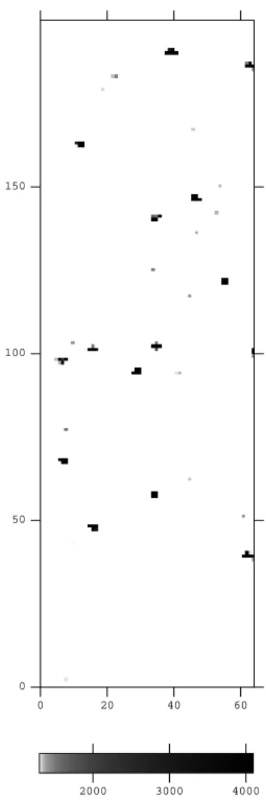
241source. The dark image appears with an offset level of about 1000 adu, and the maximum signal of 4095 adu corresponds to an energy of approximately 300 keV. The photon events show typically up in a single pixel and appear in grey color according to their relatively small energy of less than 60 keV 7KHHYHQWSDWWHUQVRIWKH - particles extend over at least four pixels and the deposited energies per pixel exceed the upper limit of the ADC.
3.3 Clock voltage amplitude
For the test of the charge handling capability a customary clock voltage amplitude of 8 V had been used. Clock voltage amplitude means the difference between the two bias voltage levels which are applied to the transfer registers VHH
1 2,
3
in Figure 1). It defines the potential well of the pixels within the transfer channel for the storage of signal electrons.
With smaller amplitude the charge storage and transfer capability will be lower because of the smaller potential barrier respectively the smaller electric field. However, small clock voltage amplitudes offer several advantages too. First of all, we achieve more operational safety because of the smaller electric fields between the transfer registers. Furthermore, faster clocking pulses can be achieved and finally, less power is dissipated.
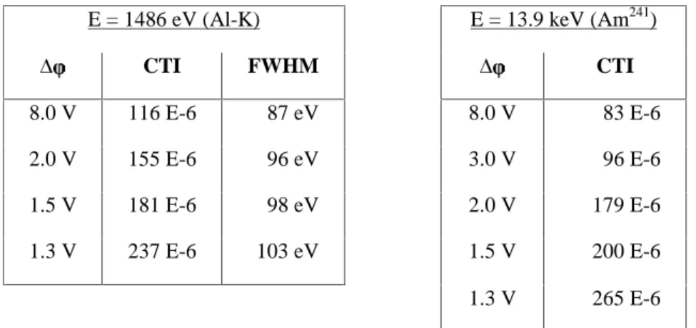
In a test series the frame store PN-CCD was operated with different clock voltage amplitudes to study the effects on
charge transfer inefficiency (CTI) and energy resolution. The results obtained for an X-ray energy of 1486 eV (Al-K
line) are summarized in Table 2 . We found, as expected, that the CTI and energy resolution degrade continuously with
smaller amplitudes. Nevertheless, even for a clock voltage amplitude of only 1.3 V, we achieve a reasonable transfer
efficiency and still a high energy resolution of 103 eV FWHM for the line.
A very small clock voltage amplitude limits, as above mentioned, the charge handling capability. For a test whether signals with an order of magnitude higher energy are already affected, we repeated the measurements with X-rays from an Am
241source. The CAMEX was again operated in low gain mode to match the energy range of the detector with the X-ray spectrum. Unfortunately, an accurate determination of the energy resolution was no more possible because one adu corresponds to an energy interval of about 100 eV in this mode. An analysis of the strongest single line in the Am
241spectrum, the 13.9 keV line, revealed a slightly stronger dependence of CTI on clock voltage amplitude compared to the previous measurements with the lower X-ray energy of 1486 eV. The moderate rise in CTI permits still high performance, even for the smallest amplitude of 1.3 V (see Table 2 ).
E = 1486 eV (Al-K) E = 13.9 keV (Am
241)
¨ CTI FWHM ¨ CTI
8.0 V 116 E-6 87 eV 8.0 V 83 E-6
2.0 V 155 E-6 96 eV 3.0 V 96 E-6
1.5 V 181 E-6 98 eV 2.0 V 179 E-6
1.3 V 237 E-6 103 eV 1.5 V 200 E-6
1.3 V 265 E-6
Table 2: CTI values of two different X-ray energies measured for diverse clock voltage amplitudes ¨ . For the detection of X-rays with an energy of 1486 eV, the detector was operated in high gain mode. This permits an accurate determination of the energy resolution, expressed as FWHM of the line. In a second test series with the CAMEX operated in low gain mode, the 13.9 keV line of an Am
241spectrum was analyzed. The CTI values increase continuously with reduction of clock voltage amplitude for both X-ray energies. Even for the smallest amplitude of 1.3 V, the frame store PN-CCD yields a relatively good charge transfer inefficiency and energy resolution. For comparison, the PN-CCD detector aboard XMM-Newton provides a CTI of 660 x 10
-6and a FWHM of 110 eV for the Al-K line.
3.4 Coating of the frame store PN-CCD chip
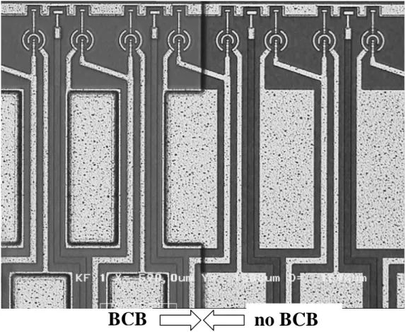
A detector application in space requires a high level of operational reliability. An enhancement in failure safety is realized for the new PN-CCD generation by coating of the chip surface. The detector is thus better protected against contamination and conductive particles which could be caused for example during assembly of the camera. We have tested a coating of the PN-CCD chip with Benzocyclobutene (BCB). BCB is a commercially available polymer dielectrics and widely used in industry e.g. for device passivation for packaging. Photo lithography is applied to structure the coating layer. Further advantages of BCB as coating material are the low curing temperature and low water absorption.
For a first test, half of the area of a PN-CCD was coated with a 3 PWKLFN%&%OD\HUH[FHSWIRUWKHUDGLDWLRQHQWUDQFH
window and the bond pads (see Figure 6). Then the chip was thermally stressed by cooling down several times to a
temperature of 130 K. The visual inspection afterwards with a microscope showed no cracks in the BCB layer and no
evidence for delamination from the CCD. During operation of the detector and in the data analysis afterwards, no
substantial performance deterioration could be observed compared to the non-coated area of the CCD chip.
Figure 6: The microscopic photograph shows a detail of the PN-CCD comprising the anodes and the circular JFETs of the on-chip electronics at top of the image and the rectangular bond pads below. The left part of the chip is covered with a 3 PWKLFN%&%OD\HU (except for the bond pads), whereas the right part is not coated. No effect of thermal stress could be observed after cooling the device down to a temperature of 130 K.
4. CAMEX READOUT CHIP
As already mentioned above, a multi-channel VLSI ASIC chip, called CAMEX64B
12, had been developed for the readout of the XMM-Newton PN-CCD detector. The chip which was fabricated with a JFET-CMOS process performs the task to amplify, filter, and multiplex 64 analog input signals of the PN-CCD in parallel. The timing of the CAMEX64B is controlled by the TIMEX chip, a custom designed ASIC chip.
An improved version of the CAMEX chip has been developed and fabricated. It is currently under test. A programmable timing generator is monolithically integrated in the new CAMEX type and takes over the function of the TIMEX chip.
This enables a larger variety of operating modes and a more compact detector assembly. Instead of 4-fold correlated double sampling like with the CAMEX64B, the new CAMEX offers 8-fold correlated double sampling (see Figure 7 ).
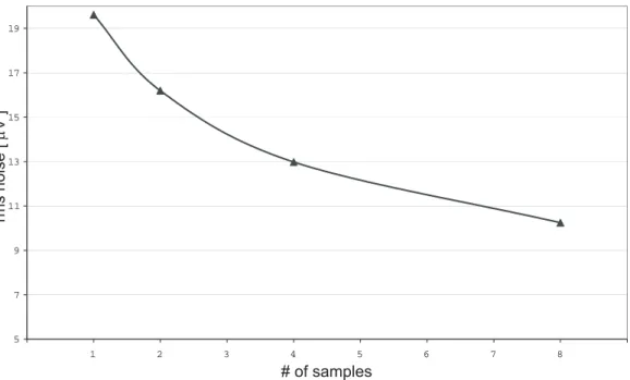
The benefit for the electronic noise resulting from a higher number of samples is demonstrated in Figure 8 . Two switchable capacitors in the amplifier stage allow a selection out of four different gains for an optimum match to the energy range of interest. The relative gain factors amount to 1, 1/5, 1/32 and 1/160 corresponding to a maximum energy of 20 keV for the highest gain and energy resolution and 3 MeV for the lowest gain, respectively. By the use of only 4 of the 8 samples, the maximum energy can be increased to 6 MeV.
The number of available input channels has been increased to 128 channels for a better match to the new CCD devices.
As a result of an optimized cable driver in the CAMEX chip, the readout speed can be increased to a rate of 10 MPixels/s.
BCB no BCB
After readout of the image, the CAMEX can be switched in standby mode to keep the power consumption and associated heat dissipation of the cooled detector small. This is of great importance for applications in space where the amount of cooling power is very small at the low detector operating temperatures between -100ºC and -80ºC. A measurement of the CAMEX power consumption (without input stage) yielded a value of 5 mW per channel for a readout speed of 6MPixel/s and in standby mode 0.2 mW per channel.
Now we evaluate the total power dissipation of 128 CCD channels with dedicated CAMEX channels. The CCD’s first FET (on-chip electronics) and the CAMEX input stage consume a power of 0.1 W during readout. The remaining CAMEX stages need, according to the measurements reported above, a power of 0.6 W at a readout speed of 6 MPixel/s and 0.03 W in standby mode.
A DUO/ROSITA detector comprises a CCD with 256 rows and two CAMEX128 preamplifiers to read out the 256 CCD channels. The cycle time was decided to 50 ms which corresponds to a frame rate of 20 images/s. With a readout time of 5 ms for the 256 rows after a warm up time of 2 ms for the CAMEX, the mean power consumption amounts to approximately 0.3 W for the detector. The focal plane is composed of seven detectors and thus we obtain about 2 W of power consumption there.
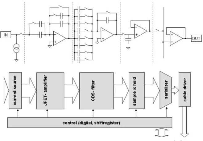
Figure 7: Block diagram of one CAMEX channel consisting of the input stage with current source, the charge sensitive
JFET-preamplifier, the correlated double sampling filter, the sample and hold stage and the serializer (multiplexer) of the 128 parallel
channels to the common cable driver. The anode of a CCD channel is connected with the gate of the on-chip JFET which is biased by
the current source of the CAMEX. The JFET amplifier stage offers two switchable capacitors which allows for a choice between four
different gains. The sampling stage (CDS-filter) consists of 8 capacitors and switches for the purpose of 8-fold sampling of the CCD
signal at the input.
5 7 9 11 13 15 17 19
1 2 3 4 5 6 7 8