Terahertz Magnetospectroscopy of Cyclotron Resonances from Topological Surface States in Thick Films of
Cd x Hg 1 x Te
Maximilian Otteneder, Daniel Sacré, Ivan Yahniuk, Grigory V. Budkin,
Kilian Diendorfer, Dmitry A. Kozlov, Ivan A. Dmitriev, Nikolay N. Mikhailov, Sergey A. Dvoretsky, Vasily V. Bel ’ kov, Wojciech Knap, and Sergey D. Ganichev*
1. Introduction
The discovery of the quantum spin Hall effect in HgTe quantum wells
[1,2]and of topological insulators
[3–5]stimulated rapidly growing interest in fundamental properties and possible applica- tions of HgTe-based materials. An attractive feature of these materials is that the band inversion, crucial for the formation
of time-reversal symmetry-protected gap- less states, can be obtained in several differ- ent ways. In particular, the topological phase transition can be realized via the var- iation of the thickness of HgTe quantum wells, by changing temperature, or by applying strain. This, together with a high quality of materials grown by molecular beam epitaxy (MBE), provides unique opportunities to study helical Dirac fermions (for reviews, see, e.g., refs. [5,6]) as well as induced superconductivity and phase-controlled Josephson junctions.
[7,8]Due to their speci fi c energy dispersion, HgTe quantum wells and strained bulk fi lms have revealed fascinating effects in magnetotransport
[2,9](for recent achieve- ments, see refs. [10 – 19]), as well as in magneto- and terahertz-spectroscopy.
[20–30]More recently, a considerable attention has been attracted to bulk Cd
xHg
1xTe fi lms with the Cd content x equal or lower than the critical one, x
c, de fi ning the phase tran- sition from inverted to noninverted band order.
[31]This interest has been driven by the observation of 3D massless Kane fermions in fi lms with x ¼ x
c,
[32]followed by detailed studies using magneto- and terahertz-spectroscopy.
[33–35]Topological insulators (TIs) based on bulk fi lms with Cd contents below
M. Otteneder, D. Sacré, K. Diendorfer, I. A. Dmitriev, S. D. Ganichev Terahertz Center
University of Regensburg 93040 Regensburg, Germany
E-mail: Sergey.Ganichev@physik.uni-regensburg.de I. Yahniuk, W. Knap
CENTERA Laboratories
Institute of High Pressure Physics Polish Academy of Sciences PL-01142 Warsaw, Poland
The ORCID identification number(s) for the author(s) of this article can be found under https://doi.org/10.1002/pssb.202000023.
© 2020 The Authors. Published by WILEY-VCH Verlag GmbH & Co. KGaA, Weinheim. This is an open access article under the terms of the Creative Commons Attribution License, which permits use, distribution and reproduction in any medium, provided the original work is properly cited.
DOI: 10.1002/pssb.202000023
G. V. Budkin, I. A. Dmitriev, V. V. Bel ’ kov Ioffe Institute
194021 St. Petersburg, Russia
D. A. Kozlov, N. N. Mikhailov, S. A. Dvoretsky Rzhanov Institute of Semiconductor Physics 630090 Novosibirsk, Russia
W. Knap
Laboratoire Charles Coulomb University of Montpellier and CNRS F-34095 Montpellier, France
Herein, studies of the cyclotron resonance (CR) in thick Cd
xHg
1xTe fi lms with different cadmium contents corresponding to materials with and without band inversion, as well as critical content corresponding to an almost linear energy dispersion are presented. The results demonstrate that the formation of 2D topological surface states requires sharp interfaces between layers with and without band inversion, in which case the corresponding CR is clearly observed for the out-of-plane orientation of magnetic fi eld but does not show up for an in-plane orientation. In contrast, all samples having more conventional technological design with smooth interfaces (i.e., containing regions of Cd
xHg
1xTe with gradually changing Cd content x) show equally pronounced CR in both in-plane and out-of- plane magnetic fi eld revealing that CR is excited in effectively 3D states. Modeling of the surface states for different fi lm designs supports main observations. In all samples, additional broad helicity-independent resonances are observed, which are attributed to photoionization and magnetic freeze-out of impurity states.
www.pss-b.com
the temperature-dependent critical x
cremain less studied so far.
[36,37]These materials, however, have a number of advantages with respect to HgTe TIs. As demonstrated by Tomaka et al.,
[36]the topologically protected surface states in Cd
xHg
1xTe are characterized by 1) two times higher Dirac fermion velocity (approximately the same as in graphene) than in pure HgTe, and 2) a larger band gap and a higher position of the Dirac point on the energy scale than that obtained in strained HgTe fi lms.
These signi fi cant advantages make TIs based on HgCdTe alloys promising for future applications.
Herein, we present a detailed study of terahertz cyclotron res- onances (CRs) of thick undoped fi lms observed in transmission, photocurrent,
[25,38]and photoconductivity.
[39]The fi lms under study are characterized by different values of the Cd content x , corresponding to both normal and inverted band order. In all samples with band inversion, two CRs have been observed in the Faraday con fi guration, where both magnetic fi eld and laser beam are oriented perpendicular to the sample surface. Evolution of these two distinct resonances with radiation frequency and helicity dependencies of the resonance amplitudes allow us to conclude that they represent CRs produced by two kinds of negatively charged carriers with slightly different masses. The cyclotron masses (below 0 : 01 m
0), obtained from the positions of the CRs, may be attributed to both bulk electrons and electrons in topological surface states, which are expected to exist in fi lms with band inversion.
Our central observations come from CR measurements in Voigt con fi guration, still with normally incident THz radiation, but with a static magnetic fi eld applied parallel to the sample sur- face. In this geometry, we obtain qualitatively different results for fi lms with abruptly changing and gradually varying Cd content x at the interfaces between layers with and without band inversion.
The combination of measurements with magnetic fi eld applied in-plane and out-of-plane provides an unequivocal experimental test on whether 2D or 3D carriers are responsible for the observed CRs. While samples with smoothly varying x manifest almost identical resonant behavior in Faraday and Voigt con fi gurations, in the sample with an abrupt transition to the cap layer one of the electron CRs disappears in the Voigt geometry. This observation clearly indicates a 2D nature of one group of electrons, apparently located at the abrupt interface and associated with a topological surface state. These conclusions are supported by theoretical modeling of the edge states in the fi lms with abrupt and smooth interfaces. Therefore, the presence of a sharp interface appears to be a crucial technological requirement for studies of fundamental topological properties of such structures.
In samples without band inversion, we detect only one CR, with a CR mass close to that calculated for the bulk material.
In all studied fi lms, we also observe an additional broad resonance located in higher magnetic fi elds. This helicity-independent reso- nance manifests slower kinetics and decays rapidly with tempera- ture. We assign this resonance to photoionization and magnetic freeze-out of impurity states.
2. Samples
The investigated samples are MBE-grown Cd
xHg
1xTe fi lms having a common general layer structure shown in Figure 1.
For each sample, a 30 nm ZnTe buffer layer was grown on top of a (013)-oriented GaAs substrate, followed by a 6 μ m layer of CdTe. After that, Cd
xHg
1xTe fi lms with different composition (as described later) and thickness ranging between 5 and 12 μ m were fabricated. All wafers were cleaved into square 5 5 mm
2samples. Ohmic indium contacts have been soldered to the sample edges and corners. In addition, for detailed magnetotransport studies, Hall bar samples were fabricated from several wafers.
Figure 1b – f shows the cadmium content x in Cd
xHg
1xTe fi lms selected for the presentation as a function of the distance d from the top of the preceding CdTe layer. In the initial step of growth of the fi lm ( d ≲ 1.5 μ m), the cadmium content x was gradually decreased to reduce the strain related to a lattice mismatch, as well as to avoid possible interface disorder effects.
Such smooth interfaces with varying x are conventionally used to improve optoelectronic and transport properties of Cd
xHg
1xTe fi lms, which are widely used for the detection of infrared radia- tion. The region of varying x is followed by a wide region with constant x ¼ 0.15 (samples #A, #B, and #C), x ¼ 0.18 (sample #D),
0 1 2 3 4 5 6
0.2 0.4 0.6
0
(a) (b) Sample #A
Cd concentration, x
Cd concentration, x Cd concentration, x
x = 0.151
Thickness, d (µm)
Thickness, d (µm)
Thickness, d (µm) Thickness, d (µm) Thickness, d (µm)
0 2 4 6 8 10 12
(f) Sample #E
x = 0.179 Cd H g
x 1-xTe
CdTe
ZnTe (013) GaAs substrate
0 1 2 3 4
0.2 0.4 0.6 0.8 1.0 0
x = 0.151 (d) Sample #C
Cd
0.85Hg
0.15Te
0 2 4 6 8
(e) Sample #D
x = 0.223 0
1 2 3 4 5
0.2 0.4 0.6
0
Cd concentration, x
0.2 0.4 0.6
0
Cd concentration, x
0.2 0.4 0.6
0 (c) Sample #B
x = 0.150
Figure 1. a) Schematic layer structure of all investigated Cd
xHg
1xTe
fi lms. b – f ) The Cd content pro fi le x ð d Þ in the top layer as a function of
the distance d from the top of the preceding CdTe layer. The values of x
in the fl at region between interfaces are indicated in the corresponding
panels. Note that unlike other structures with smoothly varying x ð d Þ ,
the sample #C in part (d) has a sharp interface between the fl at region
made of Cd
0.15Hg
0.85Te with band inversion and a 30 nm cap layer made
of Cd
0.85Hg
0.15Te without band inversion.
or x ¼ 0.22 (sample #E) which will be called the fl at region in the following. After that, a cap layer with gradually increasing Cd content was grown in all samples except for the sample #C.
In sample #C, the fl at region with x ¼ 0.15 was capped by a 30 nm layer of Cd
0.85Hg
0.15Te, which resulted in a sharp bound- ary between the fl at region with band inversion and the cap layer without band inversion.
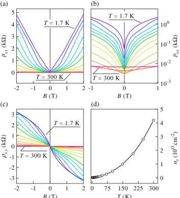
All samples were characterized by transport measurements performed using standard low-frequency lock-in technique in the temperature range from 2 to 300 K and an out-of-plane magnetic fi eld up to 10 T. For wafers with no Hall bars available, the corresponding longitudinal and Hall resistivities have been calculated from data obtained on the van der Pauw samples using permutation method. These studies established that all samples exhibit similar transport behavior that is apparently insensitive to the presence of band inversions and to the type of interfaces.
At low temperatures, all samples show strong positive magneto- resistance and a nonlinear Hall effect. A typical example is shown in Figure 2 showing the longitudinal and Hall resistivities obtained from the magnetoresistance data recorded on a Hall bar sample made from wafer #A. The slope of the Hall resistivity at low magnetic fi eld corresponds to negatively charged carriers (electrons), whereas at strong fi eld the Hall slope typically changes to a hole-like. Such behavior is conventional for electron – hole systems
[40]in conditions when the hole density exceeds the elec- tron density (although both have the same order of magnitude), whereas electrons are characterized by a signi fi cantly higher
mobility. The values of sheet densities and mobilities for different types of carriers can be extracted using the two-component classical Drude model, which was successfully implemented for thin HgTe fi lms.
[11,38,41]The values of sheet electron density n
sobtained from such modeling are shown in Table 1. In this table, we also provide the values of average volume electron density n , which are obtained from the corresponding sheet electron densities n
sas n ¼ n
s=w , where w denotes the corresponding Cd
xHg
1xTe fi lm thicknesses (Figure 1b – f ).
It should be emphasized that the aforementioned technique does not allow one to distinguish possible different groups of elec- trons (or holes) and yields the total electron and hole densities and average mobilities only. We also mention that the agreement between measured transport data and fi ts using the two-component model was not very good in the region of low magnetic fi elds.
Therefore, in Figure 2d, we present results of an alternative simpler treatment within the single-component Drude model, where the effective sheet density of electrons in the fi lm n
sis obtained from the linear slope of the Hall resistivity at low magnetic fi elds.
Overall, transport measurements demonstrate that, at low temperatures, the electron sheet density is rather small and lies in a range of n
s¼ 2 ÷ 4 10
11cm
2. The hole sheet density is slightly larger than the electron one. The holes do not contribute to the observed CRs, so their properties will not be discussed in detail. However, they play an important role in keeping the overall electroneutrality. At higher temperatures, both electron and hole densities increase, mainly because of the usual temp- erature smearing of the energy distribution, but temperature variation of the bulk energy gap may also play an important role.
[33]Typically, at 77 K, the electron sheet density reaches n
s¼ 2 ÷ 3 10
12cm
2for all samples, whereas at 300 K the density rises to n
s¼ 3 10
13÷ 1.2 10
14cm
2. It is worth noting that at liquid nitrogen temperature every sample shows an order of magnitude increase in density in comparison with low tempera- tures, and, at the same time, the values of n
sare very similar for all samples independent of the value of the band gap in the fl at region. Such behavior suggests that at T < 77 K, the bulk carriers do not play any essential role in transport and points to the for- mation of inversion/accumulation quasi-2D layers at the interfa- ces of the fi lm, or, alternatively, to the formation of topological surface states with similar properties in samples with band inver- sion. Note that in both cases the bulk holes play an important role in maintaining overall charge neutrality in the sample.
-2 -1 0 1 2
0 1 2 3 4 5
-2 -1 0 1 2
-3 -2 -1 0 1 2 3
0 75 150 225 300 0 1 2 3 4 5
-1 0 1 10
-310
-210
-110
0B (T) T = 1.7 K
T = 300 K
xy
(k )
B (T) T = 1.7 K
T = 300 K
(b)
n
s(1 0
13cm
-2)
T (K) (d)
(c)
xx
(k )
xx
(k )
B (T) T = 1.7 K
T = 300 K (a)
Figure 2. Magnetoresistivity obtained on a Hall bar made from wafer #A with x ¼ 0.15 at different temperatures, T ¼ 1.7, 10, 15, 20, 25, 30, 40, 50, 70, 100, 150, and 300 K. a,b) The longitudinal sheet resistivity ρ
xxin linear and logarithmic scale, respectively. c) The Hall resistivity ρ
xy. d) The effec- tive sheet electron density n
sð T Þ obtained from the linear slope of ρ
xyat B ¼ 0 in part (c).
Table 1. Basic parameters of the investigated samples #A – #E including the Cd content x, the corresponding type of the band order in the fl at region, type of the top interface, the effective sheet electron density n
sobtained from low-frequency magnetotransport measurements at T ¼ 4.2 K, and the corresponding average volume density n (obtained as n
sdivided by the total Cd
xHg
1xTe fi lm thickness).
Sample Cd content, x Band structure Top interface n
s½ 10
11cm
2n ½ 10
14cm
3#A 0.151 Inverted Smooth 2.9 4.8
#B 0.150 Inverted Smooth 2.2 3.7
#C 0.151 Inverted Sharp 3.3 6.7
#D 0.179 Normal Smooth 4.2 4.2
#E 0.223 Normal Smooth 2.4 1.9
3. Methods
For optical excitation, we used linearly polarized radiation from a continuous wave molecular gas laser operating at frequen- cies f ¼ 2.54 THz (wavelength λ ¼ 118 μ m, photon energy ℏω ¼ 10.5 meV), 1.63 THz ( λ ¼ 184 μ m, ℏω ¼ 6.74 meV), and 0.69 THz ( λ ¼ 432 μ m, ℏω ¼ 2.87 meV).
[40,42]The laser provided radiation power ranging between 40 and 120 mW depending on the wavelength. The radiation was modulated by an optical chopper operating at a frequency of about 80 Hz. The samples were placed in a temperature controllable optical cryostat with z -cut quartz and polymethylpentene windows. To block visible and near-infrared radiation, the windows were additionally covered by black polyethylene foil. The laser beam was focused using off-axis parabolic mirrors and controlled by a pyroelectric camera.
[43]It had an almost Gaussian shape with the spot diameter ranging from 1.5 to 3 mm depending on the wave- length. Room-temperature lambda plates made of x -cut quartz were used to modify the state of polarization, in particular, to obtain circularly polarized right-handed ( σ
þ) and left-handed ( σ
) radiation. For time-resolved measurements, we additionally used a pulsed optically pumped THz laser with a pulse duration of about 100 ns, a repetition rate of 1 Hz, and a peak power P of up to 60 kW.
[44–46]The laser emitted frequency lines in the range between 0.6 and 2.6 THz.
A split coil superconductive magnet was used to study magnetic fi eld dependencies of radiation transmission and pho- tocurrents. Most of the experiments were performed with normally incident THz radiation and magnetic fi eld oriented either perpendicular to the fi lm surface (Faraday geometry) or in-plane (Voigt geometry) (Figure 3a,b). In addition, experiments in Faraday geometry with the sample tilted by an angle θ were conducted (Figure 3c).
For experiments on radiation transmission, a pyroelectric detector was placed behind the sample (Figure 3). Photo- voltage and photoconductivity measurements were conducted
using a standard lock-in technique. Photovoltage was measured using the phase-locked voltage drop across the sample under the in fl uence of the chopper-modulated THz radiation in the absence of external DC bias. To measure the photoconductivity, an external DC bias was applied and photoresponses for positive and negative bias polarities were subtracted to exclude photogal- vanic contributions and extract the photoconductivity signal.
Alternatively, in some photoconductivity measurements, we applied a low-frequency AC bias and used a double-modulation technique described in previous studies.
[39,47]Because main conclusions of this work are based on the com- parison of results obtained using the three setups in Figure 3, it is important to recall the basic distinctions between them in application to 3D and 2D electron systems. In a 3D system, CR is expected to emerge in all three setups; the orientation of both the laser beam and static magnetic fi eld with respect to the sample surface is immaterial for a 3D isotropic system;
the dynamics of carriers is different for parallel (Faraday) and perpendicular (Voigt) relative orientation of the magnetic fi eld and THz radiation propagation directions. This different dynam- ics may lead to a substantial shift of the resonance position in Voigt geometry with respect to Faraday geometry (see ref. [48]
and Section 5 for details).
For a 2D system localized at an interface parallel to the sample surface, the decisive role is played by the orientation of the mag- netic fi eld with respect to the surface. Only the normal compo- nent of the magnetic fi eld affects the in-plane dynamics of carriers and leads to the development of the cyclotron motion and the formation of Landau levels. In contrast, the in-plane static magnetic fi eld can only slightly modify the con fi nement energy and the corresponding common wave function describing the localized 2D electron states. In the case of normal orientation of magnetic fi eld (as in Faraday geometry in Figure 3a), one thus expects a usual CR dip in transmission for both 2D and 3D elec- trons. On the contrary, for in-plane magnetic fi eld (as in Voigt geometry in Figure 3b) 2D electrons should manifest no CR, whereas 3D electrons can still experience CR.
4. Results
4.1. Cyclotron Resonances in Cd
0.15Hg
0.85Te Films with Band Inversion and Smooth Interfaces
We begin with the presentation of results of magnetotransmis- sion and photovoltage measurements performed on almost identical Cd
0.15Hg
0.85Te fi lms #A and #B (Figure 1b,c). The fl at layer in both samples has a Cd content x ≃ 0.15, corresponding to inverted bands for temperatures below T ≃ 90 K.
[33]On both sides of the fl at layer, the Cd content gradually increases, thus providing smooth interfaces to regions without band inversion.
Magnetotransmission data recorded in Faraday geometry (Figure 3a) for samples #A and #B are presented, correspond- ingly, in Figure 4 and Figure 5. The data here and later generally manifest three resonant dips for both negative and positive values of the out-of-plane magnetic fi eld B . The positions of observed resonances at B ¼ B
CR1,2, B ¼ B
CR, and B ¼ B
i, marked by arrows in Figures 4 and 5, are always symmetrically offset from the origin B ¼ 0.
(b) (a)
o t c e t e d r
o t c e t e
d r
t g i o V y
a d a r a F
(c) V
phV
phV
phdetector B B
B
Faraday with tilted sample
Figure 3. Experimental setups for transmission and photovoltage measurements: a) Faraday con fi guration with both magnetic fi eld and the incident THz beam oriented along the normal to the sample surface;
b) Voigt configuration with an in-plane magnetic field; c) Faraday configu-
ration with the sample being tilted by an angle θ with respect to the
common direction of the laser beam and magnetic field.
The main focus of this work concerns the sharp dips at low B which, as shown later, originate from the CR of free conduction electrons. In contrast, the broad minima at B ¼ B
iare attrib- uted to photoionization of impurities and will be addressed separately in Section 4.4. The data in Figures 4 and 5a show that the low- fi eld resonances are sensitive to the radiation helicity.
Although, for the right-handed circular polarization σ
þ, they appear only at positive B , for the left-handed circular polarization σ
, they are present at negative B only. The position of these res- onances scales linearly with the radiation frequency (Figure 5b).
All these features indicate that the low- B sharp dips are indeed caused by the CR of negatively charged free carriers.
More speci fi cally, magnetotransmission traces in Figure 4a that were recorded at the highest radiation frequency f ¼ 2.54 THz show two distinct sharp dips at B ¼ B
CR1and B ¼ B
CR2, which clearly reveals the presence of two kinds of electrons with different cyclotron masses (the corresponding values are shown in Table 2). It is worth mentioning at this point that the corresponding cyclotron masses below 0 : 01 m
0may be attributed
both to bulk electrons and electrons in topological surface states, which are expected to exist in the fi lms with inverted bands. At lower frequency f ¼ 1.63 THz, the CR dips start to merge, and become indistinguishable at the lowest frequency f ¼ 0.69 THz where a single merged CR dip B
CRis observed (Figure 4b,c). The positions of the resolved CR dips for f ¼ 2.54 THz and f ¼ 1.63 THz are found to be almost identical for both samples
#A and #B (Figures 4 and 5 and Table 2).
Solid lines in Figure 4 show magnetotransmission fi ts obtained using a two-component Drude model with account for interference effects due to multiple re fl ections in the substrate. Speci fi cally, the complex THz conductivity σ is mod- eled as a sum of contributions σ
jfrom each electron transport channel j , with individual σ
jgiven by the Drude formula σ
j¼ en
sjμ
1jþ iðB
CRjBÞ (1)
Here, e is the elementary charge, n
sjand μ
jare the electron sheet density and mobility in the transport channel j , B
CRj¼ m
j2 πf =e de fi nes the position of CR for a given THz frequency f through the cyclotron mass m
j, and the þ ( ) sign before B corresponds to the left-handed (right-handed) circular polarization of the THz radiation. The fraction of transmitted power in Faraday geometry is then expressed through σ ˜ ¼ σ= 2 ϵ
0c as
[49,50]TðBÞ ¼
ð 1 þ σÞ ˜ cos ϕ i 1 þ n
2rþ 2 σ ˜ 2 n
rsin ϕ
2(2)
-2 -1 0 1 2
0.5 1.0
0
-2 -1 0 1 2
0.4 0.6 0.8 1.0
-2 -1 0 1 2
0.5 1.0
0
− +
f = 2.54 THz (a)
B
CR1transmission, transmission, transmission,
− +
f = 1.63 THz (b)
B
iB
CR2B
iB
CR2B
CR1magnetic field, B (T)
− +
(c)
f = 0.69 THz B
CRB
iFigure 4. Magnetotransmission normalized to its maximal value for sam- ple #A with band inversion in the flat region. Measurements were done in Faraday geometry (Figure 3a) at T ¼ 4.2 K using σ
þand σ
polarized radi- ation at three different frequencies: a) f ¼ 2.54 THz, b) f ¼ 1.63 THz, and c) f ¼ 0.69 THz. In all panels, the experimental data points are shown by circles, whereas the solid lines present the fits described in the text. In all cases, we observe sharp deep minima at positions of CRs [B ¼ B
CR1and B ¼ B
CR2in (a,b), and B ¼ B
CRin (c)], see arrows marked at the posi- tive B side. These CRs show up at either positive or negative B depending on the helicity of incoming radiation. At higher B, we observe symmetric wide minima centered at B ¼ B
i, which are not sensitive to the radiation helicity. The resonance field values and corresponding cyclotron masses are shown in Table 2.
0 1 2 3
0.5 1.0 1.5
0
-2 -1 0 1 2
0.5 1.0
0
resonance field (T)
radiation frequency, f (THz) B
iB
CR1B
CR2sample #A
sample #B
− +f = 1.63 THz
B
iB
CR2B
CR1magnetic field, B (T) sample #B
transmission,
(a)
(b)
Figure 5. a) Normalized magnetotransmission of f ¼ 1.63 THz radiation
measured on sample #B in Faraday geometry at T ¼ 4.2 K. Two well-
resolved CR dips emerge at either B ¼ B
CR1,2or B ¼ B
CR1,2depending
on the helicity (σ
þor σ
) of incoming radiation. Additional helicity insen-
sitive resonances are detected at B ¼ B
iin both traces. Solid lines are
fits according to Equation (2) including additional Lorentzians at B
i.
b) Magnetic field positions of the observed resonances B
CR1, B
CR2, and
B
i(as marked) plotted against radiation frequency for samples #A (circles)
and #B (stars) (see also Table 2). Dashed lines present linear fits to the data.
where ϕ is the interference phase accumulated after single re fl ec- tion in the substrate, n
ris the refractive index of the substrate, ε
0the permittivity of free space, and c the speed of light. Using Equation (2), we were able to precisely fi t all magnetotransmis- sion traces. This demonstrates that the model based on Drude approximation is capable to reproduce the experimental observa- tions. At the same time, the magnetotransmission traces do not provide suf fi cient data to convincingly extract all relevant param- eters of the model. The fi ts to experimental data required an addi- tional constant offset accounting for nonresonant contributions of other transport channels. Two identical Lorentzians centered at B ¼ B
iwere included into the model to account for the impu- rity resonances discussed in Section 4.4.
The CRs were also detected in photovoltage experiments.
A typical photovoltage trace, shown in the inset of Figure 6a, features two peaks coinciding with the positions of the CR dips in magnetotransmission as indicated by vertical dashed lines.
Similar to the transmission dips, the position of the peaks scales linearly with the radiation frequency (Figure 6a). Note that, in the photovoltage response, two CR peaks are clearly resolved even for the lowest frequency f ¼ 0.69 THz, in which case the CR dips in magnetotransmission get merged (Figure 4c).
Strikingly, applying a tilted magnetic fi eld (see the experimen- tal setup in Figure 3c), we obtain that the CR positions are inde- pendent of the tilt angle θ (Figure 6b). This observation provides a fi rst clear evidence that the resonances are excited in a 3D elec- tron gas. Indeed, for a 2D system, one would expect a signi fi cant up-shift of the resonance position with the increase in the tilt angle because in this case the CR should be sensitive only to the normal component of the magnetic fi eld. Here, it is important to stress that the tilted fi eld measurements are performed in Faraday geometry, in which case the resonance position for an isotropic 3D system is expected to be independent of the tilt angle.
Measurements of the magnetotransmission in Voigt geometry (Figure 3b) con fi rm the aforementioned conclusions showing that even for a magnetic fi eld oriented in-plane both CRs are still present (Figure 7). This observation rules out the possibility that any of the observed resonances originates from 2D electrons.
We note that, as expected, in Voigt geometry, the CR dips become helicity-independent and show up symmetrically for two polarities of magnetic fi eld. The CR fi eld values detected for sample #A are found to be slightly smaller in Voigt geometry than in Faraday geometry, which could be attributed to the 3D Table 2. Magnetic-field positions of resonances and corresponding cyclotron masses extracted from magnetotransmission and photovoltage traces obtained at T ¼ 4.2 K. Note that resonances marked with an asterisk were visible in photovoltage only, and were not resolved in magnetotransmission.
Sample Cd content x Frequency, f ½THz B
CR1½T or B
CR½T B
CR2½T B
i½T B
VCR1½T or B
VCR½T B
VCR2½T m
CR1½ m
em
CR2½ m
e#A 0.15 2.54 0.38 0.50 1.45 0.0042 0.0055
1.63 0.20 0.27 0.77 0.16 0.24 0.0035 0.0046
0.69 0.09* 0.11 0.52* 0.0035 0.0044
#B 0.15 2.54 0.33 0.49 1.25 0.36 0.50 0.00365 0.0053
1.63 0.20 0.28 0.92 0.20 0.28 0.0034 0.0047
#C 0.15 2.54 0.30 0.46 1.35* 0.46 – 0.0033 0.0051
#D 0.22 2.54 0.81 – 2.33* 0.82 – 0.0089 –
1.63 0.49 – 1.45* 0.45 – 0.0084 –
#E 0.18 2.54 0.28 – 0.77* 0.0031 –
0.69 0.065 – 0.25* 0.0026 –
0 1 2 3
0.5 1.0 1.5
0
0 10 20 30 40 50
0.2 0.4 0.6 0.8 1.0
0
0.2 0.4 0.6 -0.1 0.0 0.1 0.2 0.3
resonance field (T) resonance field (T)
radiation frequency, f (THz)
B
CR1B
CR2B
iB (T)
tilt angle, (°) f = 1.63 THz
B
iB
CR2B
CR1V
ph(mV)
f = 2.54 THz
B
CR2B
CR1(a)
(b)
Figure 6. a) Resonance field values B
CR1, B
CR2, and B
i(as marked) extracted from photovoltage measurements on sample #A at T ¼ 4.2 K in Faraday configuration. The low-B part of a typical photovoltage trace, obtained at radiation frequency f ¼ 2.54 THz, is shown in the inset.
b) Dependence of the resonance field values on the tilt angle obtained
from photovoltage measurements on sample #A at T ¼ 4.2 K under f ¼
1.63 THz radiation in the Faraday con fi guration with tilted sample
(Figure 3c). Dashed lines are linear fits to the data.
plasmonic shift (see ref. [48] and Section 5). Surprisingly, such shifts were not detected for other samples (Table 2).
4.2. Cyclotron Resonances in Cd
0.15Hg
0.85Te Film with Band Inversion and Sharp Top Interface
For sample #C, the behavior of resonances becomes qualitatively different despite the fact that this sample has almost the same design and that the Cd content in the fl at region remains the same as in samples #A and #B. The only difference is that, instead of a smooth top interface as in samples #A and #B, sam- ple #C has an abrupt boundary between the Cd
0.15Hg
0.85Te fi lm and the Cd
0.85Hg
0.15Te cap layer (Figure 1d).
Similar to samples #A and #B, in Faraday geometry, sample
#C clearly manifests two CRs in both magnetotransmission (see, e.g., blue curve in Figure 8a) and photovoltage (Figure 8c).
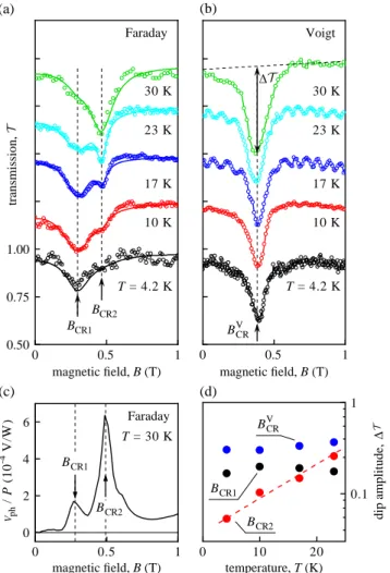
However, in sharp contrast to samples with two smooth interfa- ces, in Voigt con fi guration only one CR dip remains (Figure 8b).
The fact that one of the resonances disappears in Voigt geometry provides a clear evidence that it originates from 2D con fi ned elec- tron states. Figure 8d shows the temperature dependence of the dip amplitude ΔT . For resonances at B
CR1(Faraday geometry) and B
VCR(Voigt con fi guration), we observe that ΔT is almost independent of temperature. In contrast, the strength of the CR resonance at B
CR2, which is present in Faraday geometry only, strongly increases with rising temperature. Such tempera- ture evolution is strikingly similar to that found recently for topological surface states in strained 80 and 200 nm HgTe fi lms.
[25,38]Taken together, the aforementioned observations clearly indicate the formation of 2D surface states at the abrupt interface between materials with and without band inversion.
4.3. Cyclotron Resonances in Films without Band Inversion
We proceed to results obtained on fi lms #D (with x ¼ 0.22) and
#E ( x ¼ 0.18) which are expected to have normal band order.
Indeed, the data we are going to discuss were obtained at liquid helium temperature at which the critical Cd content marking the
transition from normal to inverted band order is x
c≃ 0.17.
[33,51]Thus, in both samples, the Cd content in the fl at region is higher than x
cmeaning that they should behave as conventional narrow- gap semiconductors.
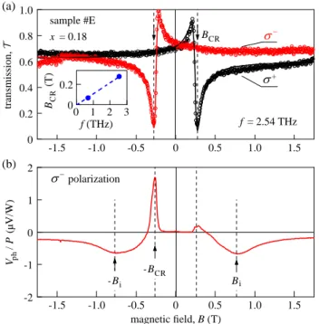
In contrast to previously discussed materials with x ¼ 0.15, for these samples, we observe a single CR in both Faraday and Voigt geometries. Magnetotransmission data for samples
#D and #E is shown in Figure 9a,b and Figure 10a. The data in Figure 9a,b are obtained with linearly polarized THz radiation.
Correspondingly, the CR dip is present for both polarities of magnetic fi elds. For circularly polarized radiation, the CR dip appears either in positive ( σ
þ) or negative ( σ
) B (Figure 10a).
It is worth mentioning that the CR positions and the corre- sponding cyclotron masses obtained on samples #D and #E (see Table 2 and insets in Figures 9 and 10) are substantially
0.5 1
0.50 0 0.75 1.00
10 K 17 K 23 K 30 K
Voigt Faraday
B
CR1B
CR2magnetic field, B (T) magnetic field, B (T)
magnetic field, B (T)
0.5 1
0 T = 4.2 K
10 K 17 K 23 K 30 K
T = 4.2 K
B
VCR0 10 20
0.1 1
dip amplitude, '
temperature, T (K) B
CR2B
CR1B
VCR'
0.5 1
0 0 2 4 6
Vph
/ P (10
-4V/ W )
T = 30 K Faraday B
CR1B
CR2transmission,
(a) (b)
(d) (c)
Figure 8. Normalized magnetotransmission of f ¼ 2.54 THz radiation obtained on sample #C at different temperatures (as marked) in a) Faraday and b) Voigt con fi gurations. Traces are vertically offset by 0.25 for better visibility. Solid lines in part (a) are fi ts using Equation (2). c) Photovoltage measured on sample #C in Faraday con fi guration at T ¼ 30 K. d) Temperature dependence of the amplitudes ΔT of the CR dips at B
CR1,2and B
VCR(as marked) extracted from the magnetotrans- mission data presented in parts (a) and (b). The dashed line shows a linear fi t for the amplitude of the CR dip at B
CR2. The corresponding CR fi eld values are shown in Table 2.
-1.5 -1.0 -0.5 0 0.5 1.0 1.5
0.6 0.8 1.0
magnetic field, B (T) f = 1.63 THz Voigt
- +
B
CR1VB
VCR2B
iVtransmission,
Figure 7. Normalized magnetotransmission of f ¼ 1.63 THz radiation measured in Voigt configuration on sample #A at T ¼ 4.2 K. Two pairs of well resolved CR dips emerge symmetrically at B ¼ B
VCR1,2and B ¼ B
VCR1,2for both circular polarizations σ
þ(black curve) and σ
(red curve).
Additional broad resonances are detected at B ¼ B
iin both traces.
All resonance field values are shown in Table 2.
different from those obtained on the other samples with x ¼ 0.15. This is consistent with our expectations: the largest cyclotron mass is obtained for sample #D with x ¼ 0.22 which is supposed to have the largest band gap, whereas the lowest mass is obtained for sample #D with x ¼ 0.18, closest to the criti- cal Cd content x
c≃ 0.17 corresponding to a gapless material with a linear spectrum. We also mention that a strong asymmetry of the CR feature in Figure 10a is well captured by our fi tting model and manifests signi fi cant role of interference effects included into Equation (2). Indeed, according to this formula, a symmetric shape of the transmission dip is expected either in conditions of constructive interference (sin ϕ ¼ 0) or destructive interference (cos ϕ ¼ 0). For intermediate values of ϕ , the shape can be highly asymmetric,
[49]and the observation of such strong asymmetry is a clear indication of the importance of interference effects.
The CRs were also detected in the photovoltage response.
Under linearly polarized radiation as in Figure 9c, two symmetric CR peaks emerge in positive and negative B , whereas the circu- larly polarized radiation in Figure 10b gives rise to a single pronounced CR peak for the corresponding active magnetic fi eld polarity only. In this particular case, an additional peak with sub- stantially smaller magnitude was detected for the CR passive
magnetic fi eld B > 0, most probably caused by parasitic antenna effect produced by contact wires.
4.4. Impurity-Related Resonances
Apart from the sharp CRs at low jBj which constitutes the main subject of this work, all samples manifested broad resonant features at higher magnetic fi elds which, as discussed later, can be naturally attributed to photoionization of impurities and thus are referred here as impurity resonances. The main properties of the impurity resonances, observed in magneto- transmission as well as in photovoltage and photoconductivity, can be summarized as follows. First of all, impurity resonances appear symmetrically with respect to B ¼ 0 at B ¼ B
iin both Faraday and Voigt geometries, and are insensitive to the radia- tion helicity (Figure 4). This fact alone provides a clear evidence that they may not be caused by the CR. The resonance positions B ¼ B
iscale linearly with radiation frequency, as exempli fi ed for samples #A and #B in Figure 5b. In contrast to the CR, in which case the amplitude of dips in transmission is either inde- pendent of temperature or increases with rising T , the amplitude of dips at B ¼ B
idecreases quickly with growing T and vanishes at T 30 K (Figure 11a). The position B
iof impurity resonances shifts to lower jBj as T grows (Figure 11b), whereas the CR positions are T -independent. The photoconductivity sig- nal, as shown in Figure 11c, signi fi cantly increases around the position of the impurity resonance. The positions of impurity resonances for a given radiation frequency are substantially 0
0.90 0.95
1.00 sample #D
Faraday
B
CRx = 0.22
f = 1.63 THz
1 . 0 1 . 5
0.7 0 0.8 0.9 1.0
Voigt
B
CR V0 1 2 3
0.5 1.0
0
R
B
C(T)
f (THz)
-1.5 -1.0 -0.5 0.5 1.0 1.5
-1.5 -1.0 -0.5 0.5
-3 -2 -1 0 1 2 3
-0.5 0.5 1.0
0
magnetic field, B (T) V
ph(mV)
B
CRFaraday
B
itransmission,
(a)
(b)
(c)
transmission,
Figure 9. Normalized magnetotransmission of f ¼ 1.63 THz linearly polarized radiation recorded on sample #D without band inversion (x ¼ 0.22) at T ¼ 4.2K in a) Faraday and b) Voigt con fi gurations. Solid lines in part (a) are fi ts using Equation (2). c) Photovoltage measured under the same conditions in Faraday con fi guration. The inset shows the CR fi eld extracted from data obtained in Faraday con fi guration for two frequencies. All resonance fi eld values are shown in Table 2.
0.2 0.4 0.6 0.8 1.0
0
0 1 2 3
0.2 0
-1.5 -1.0 -0.5 0 0.5 1.0 1.5
-1.5 -1.0 -0.5 0 0.5 1.0 1.5
-2 -1 0 1 2
sample #E
−B
CRf = 2.54 THz
+
B
CR(T)
f (THz)
magnetic field, B (T) V
ph/ P (µV/W)
x = 0.18
-B
CR-B
i −polarization
B
itransmission,
(a)
(b)
Figure 10. a) Magnetotransmission of circularly polarized f ¼ 2.54 THz
radiation measured on sample #E with x ¼ 0.18 in Faraday geometry
at T ¼ 4.2 K. The CR fi elds extracted from magnetotransmission data
display a linear frequency scaling shown in the inset. b) Photovoltage
measured under the same conditions for σ
polarization. The extracted
resonance fi eld values are shown in Table 2.
different for samples with different cadmium content x (Table 2).
In samples with x ¼ 0.15 in the fl at region (with band inversion), the impurity resonances were detected both in transmission and photovoltage, whereas in samples with x > x
c(without band inversion) they were present in photovoltage but not visible in magnetotransmission.
On a qualitative level, the aforementioned features are consis- tent with the photoionization mechanism if one considers that the activation energy of shallow impurities can signi fi cantly increase in magnetic fi eld, an effect well-known as magnetic freeze-out of impurities.
[52]In this scenario, in the limit of low B , the activation energy is so small that all impurities are thermally ionized making the photoionization processes impos- sible.
[53]In stronger jBj , the activation energy of impurities increases such that at suf fi ciently low T the majority of impurities are in the neutral state and, at the same time, the photon energy is high enough to promote electrons into the unbound states in the conduction band. Under the same conditions, the total occupation of the conduction states is lowered making the rela- tive contribution of the photoexcited carriers more pronounced.
This is the parametric region of the impurity resonance where one expects most remarkable in fl uence of the photoioni- zation processes on magnetotransmission and photovoltage signals. In still stronger jBj and low T , the photoionization is blocked as soon as the energy distance between the ground level of impurity and available unbound states exceeds the photon energy. Photoionization is thus possible in an intermediate range of jBj centered at a certain B
i, and should be effective at suf fi ciently low temperatures only. Furthermore, the position of B
ishould increase with the radiation frequency, and should
also be highly sensitive to temperature and to the Cd content x , as both of them modify the spectrum and, therefore, the posi- tion of impurity levels. On top of that, the temperature depen- dence can be affected by the processes of photoexcitation between the hydrogen-like impurity levels with subsequent thermal excitation into the continuum of unbound conduction states.
[54,55]Assuming that the resonance at B
iis related to the ionization of impurity states, it is also natural to expect different kinetics of the photoresponse with respect to that at CR. These expecta- tions were con fi rmed by time-resolved photoconductivity measurements performed using a pulsed THz laser. Figure 12 shows that indeed the decay of the photoresponse at the posi- tion B ¼ B
iof the impurity resonance is several times longer than that measured at the position B ¼ B
CRof CR. In the latter case (black trace in Figure 12), the photosignal essentially reproduces the form of the THz laser pulse (data not shown), meaning that kinetics of free carriers responsible for the CR is fast on the time scale of pulse duration, given by the full width at half maximum τ
pulse≃ 100 ns. In contrast, the photo- signal measured at B ¼ B
i(red trace in Figure 12) features a sig- ni fi cant long-time tail, which can be well fi tted by an exponential function exp ðt=τÞ (blue line in Figure 12) with a decay time τ ¼ 350 ns.
0 10 20 30
1.3 1.4 1.5
0 10 20 30
0.2 0.4 0.6
0
0.8 1.2 1.6 2.0 0 2 4 6 8
B
i(T)
T (K) ( B
i)
B '
B
i/ (10
-3)
magnetic field, B (T) T = 4.2 K
B i (a)
(b)
(c)
Figure 11. a) Temperature dependence of the amplitude of Lorentzian dips in magnetotransmission around the impurity resonance at B ¼ B
i, extracted from data measured on sample #A at f ¼ 2.54 THz as illustrated in the inset. b) Temperature dependence of the impurity resonance posi- tion B
iextracted from the same data. c) Photoconductivity Δσ normalized to the dark DC conductivity σ showing a resonant peak at position B ¼ B
iof the impurity resonance. These data were obtained at T ¼ 4.2 K on sample #A under f ¼ 2.54 THz radiation with an applied cur- rent of 100 μ A.
0.2 0.4 0.6 0.8 1.0
0 0.2 0.4 0.6 0.8 1.0
0
at B = B
CRat B = B
iΔ t
FWHM pulsenormalized photoresponse, U
= 350 ns
time, t (µs)
~ e
- /tFigure 12. Time-resolved photoconductivity response U ∝ Δσ (normal- ized to its maximum value) obtained on sample #A at liquid helium temperature using a pulsed THz laser operating at f ¼ 2.03 THz.
The black curve demonstrates a fast photoresponse at magnetic field
B
CR¼ 0.29 T corresponding to the CR. The full width at half maximum
of the CR photoresponse, Δ t
FWHM≃ 100 ns, coincides with the corre-
sponding width τ
pulseof the laser pulse pro fi le (data not shown). In
contrast, the photoresponse recorded at magnetic field B
i¼ 1T, corre-
sponding to the impurity resonance (red curve), shows a much slower
decay which can be well fi tted by an exponential function exp ð t =τÞ
(blue line) with a decay time τ ¼ 350 ns.
5. Discussion
We now return to the main observation: a qualitatively different behavior of one of the CRs in samples with sharp and smooth interfaces between materials with and without band inversion (Sections 4.1 and 4.2). The fact that one of the CRs disappears in the Voigt geometry for sample #C with a sharp interface is a clear indicator of the true 2D nature of carriers causing this resonance. The emergence of at least one surface state is indeed guaranteed by the topologically nontrivial transition from inverted to normal band order at the interface. In Faraday geometry, the same resonance exhibits a strong temperature dependence, which additionally distinguishes it from other res- onances, which are present in both Voigt and Faraday geometries and presumably originate from carriers localized at smooth interfaces. These results indicate that smooth interfaces lead to the emergence of multiple surface states, known as Volkov – Pankratov states (VPS).
[16,19,56,57]As the number N of these states is not fi xed by topology (apart from the requirement N ≥ 1), their number and properties should be sensitive to a particular choice of materials, growth conditions, form of interfaces, strain pro fi le, and so on. The dynamics of carriers occupying multiple VPS can be effectively 3D, similar to conventional quasi-2D elec- trons occupying multiple sub-bands in a wide quantum well, which would immediately explain our observations.
Before presenting model calculations supporting this interpre- tation of the distinct behaviors at smooth and sharp interfaces, we fi rst shortly comment on the observed frequency dependen- cies of the CRs and on the expected difference of resonance positions in Faraday and Voigt geometries. Both aspects deserve further systematic studies but do not in fl uence our qualitative results and conclusions, and thus are of secondary importance for the purposes of the current work.
An inspection of the results presented in Figures 5, 6, 9, 10 and Table 2 shows that the magnetic fi eld positions of CRs in all cases fairly well follow a linear frequency dependence. These observations seemingly con fl ict the well-known fact that in sys- tems with linear spectrum the energies of individual transitions between Landau levels scale as B
1=2.
[58]In fact, even for massless Dirac quasiparticles, the linear dependence should approxi- mately restore in the quasiclassical limit of high chemical poten- tial, such that many Landau levels are occupied, and the distance between them in the vicinity of the chemical potential is well described by the cyclotron mass.
[59,60]Such a classical description works well for all frequencies used in our work. Unfortunately, the presence of surface states and several types of carriers makes a reliable determination of the actual position of the chemical potential in our structures problematic. We expect that a reliable experimental evidence for the quantum square root scaling would require CR measurements in a broader frequency range.
As mentioned previously in Sections 3 and 4.1, for 3D elec- trons, the position of CR in Voigt geometry B
VCRis expected to be down-shifted with respect to the CR position B
CRin Faraday geometry. Speci fi cally, the resonance condition is given by ω
2¼ ω
2pþ ω
2cin Voigt geometry, instead of the usual ω
2¼ ω
2cin Faraday geometry.
[48]Here, ω
2p¼ ne
2=mε is the square of the plasma frequency of a 3D electron gas. Using for a rough esti- mate, the values ε
r¼ ε=ε
0≃ 10 for the relative permittivity and m=m
0¼ 0.004 for the effective mass (Table 2) in the expression
B
VCR=B
CR¼ ð 1 ω
2p=ω
2Þ
1=2, for sample #A one fi nds that the observed relative shifts B
VCR=B
CR≃ 0.8 correspond to the electron volume density n ∼ 5 10
14cm
3, in a reasonable agreement with estimates obtained from the analysis of magnetotransport data (Table 1). At the same time, this agreement can be a coinci- dence because for other samples we generally do not observe any sensible difference between the CR positions in both geometries (Table 2). These surprising fi ndings require further analysis and focused experiments. In particular, it would be interesting to understand how such plasmonic shifts are modi fi ed in the relevant case of a quasi-2D system involving several populated 2D sub-bands at the interface.
The surface states in systems with sharp interfaces are well studied for strained HgTe fi lms.
[9,25,61,62]These topologically protected states are caused by the inversion of Γ
6and Γ
8bands at the interface. The energy of the surface states depends on the wave vector k
kin the interface plane and lies in the interval between the corresponding energy levels of the light and heavy holes.
[9,63]If the crystal is strained, there is a gap between the light- and heavy-hole sub-bands; the energy of the lowest k
k¼ 0 topological surface state coincides with the top of the heavy-hole sub-band, whereas in the limit jk
kj ! ∞ the dispersion of the high-energy surface states approaches that of the light holes.
As a result, ideally, the low-temperature transport properties of a strained HgTe fi lm with the Fermi energy lying in the gap between the light- and heavy-hole sub-bands should be solely determined by the topologically protected surface states because
(b) (a)
E
c(z)
E
v(z) E
c(z)
E
v(z)
bulk lh
bulk hh bulk lh
bulk hh
VPS
single state
Figure 13. Illustration of the edge states forming at a) sharp and
b) smooth interfaces. Light blue lines with filled area below them
show the calculated probability density distributions for the edge states
in both cases. The sharp interface hosts a single well-localized topologi-
cally protected state, whereas the smooth interface gives rise to multiple
VPS, which are weakly localized in space. Red and blue lines show the real
space profiles E
vð z Þ and E
cð z Þ of the corresponding band edges. The edge
states emerge in the range between energies of the bulk light and heavy
holes, which are shown by green and magenta dashed lines and are
marked as “bulk lh” and “bulk hh,” correspondingly.
all bulk states in this case are gapped. Here, it is important to mention that, despite the very existence of a topological surface state stems from the inversion of light-hole band and conduction band at the interface, the dispersion of the surface states is strongly affected by hybridization with the heavy holes.
CdHgTe fi lms with band inversion share the aforementioned qualitative properties of strained HgTe fi lms, but usually feature much smaller band gaps which are controlled by the Cd content of the alloy.
For a smooth interface between materials with and without band inversion, the situation is different. The calculations below show that instead of a single topologically protected state, the interface now can host multiple VPS.
[16,19,56,57]Similar to the case of the sharp interface, the energies of VPS lie in between the energies of the strain-split light and heavy holes. Figure 13 schematically shows a sharp interface (as in sample #C, Figure 13a) and a smooth interface (as in sample #A or #B, Figure 13b). The left parts in Figure 13a,b present the fl at Cd
0.15Hg
0.85Te regions, whereas the middle parts show the tran- sition to the top cap layer without band inversion and with a larger band gap sketched in the right parts. For the sharp inter- face, the spatial extension of the topologically protected surface state is determined by an exponential decay of the wave function inside both the fi lm and the barrier. In contrast, the extension of VPS localized at a smooth interface is governed by the spatial gradient of the band gap near the band inversion point. The spa- tial distribution of the probability densities for the corresponding wave functions is illustrated in Figure 13. If one increases the width of the transition region between the topological insulator and normal insulator, both the total number of the VPS and their widths increase. This explains why two samples #A and #C with an almost identical design, but different interface structures, show different behavior in the Voigt con fi guration. Sample #C hosts 2D topologically protected states which do not experience CR in an in-plane of the interface magnetic fi eld, whereas sample
#A exhibits behavior typical for a quasi-2D system with many occupied sub-bands.
For numerical calculations, we implemented the six-band Kane model taking into account a static strain of the crystal which causes a splitting of the heavy- and light-hole sub-bands. In the basis of the Γ
6and Γ
8states, the Kane Hamiltonian has the form
[64]H ¼ E
cI
2H
cvH
†cvE
vI
4þ H
BP!
(3)
where I
nis the n n identity matrix and
H
†cv¼ P
cv0 B B B B B B B B
@
kxpikffiffi
2y0 ffiffi
23
q
k
z kxpikffiffi
6ykxpþik
ffiffi
6yffiffi
2 3