nanoribbons from different perspectives
Dissertation
zur Erlangung des Doktorgrades der Naturwissenschaften (Dr. rer. nat)
der Fakultät Physik der Universität Regensburg
vorgelegt von
Tobias Preis
aus München
im Jahr 2020
Prof. Dr. Jascha Repp Prof. Dr. Dieter Weiss
Prüfungsausschuss:
Vorsitzender: Prof. Dr. Jaroslav Fabian
Erstgutachter: PD Dr. Jonathan Eroms
Zweitgutachter: Prof. Dr. Jascha Repp
weiterer Prüfer: Prof. Dr. Christoph Strunk
1. Introduction 5
2. Theoretical basics 7
2.1. Graphene nanoribbons . . . . 7
2.1.1. Graphene . . . . 7
2.1.2. Lattice and electronic structure of graphene nanoribbons . . . 10
2.1.3. Fabrication of graphene nanoribbons . . . 17
2.2. Scanning Probe Microscopy . . . 19
2.2.1. Scanning Tunneling Microscopy . . . 19
2.2.2. Scanning Tunneling Spectroscopy . . . 22
2.2.3. Atomic Force Microscopy . . . 23
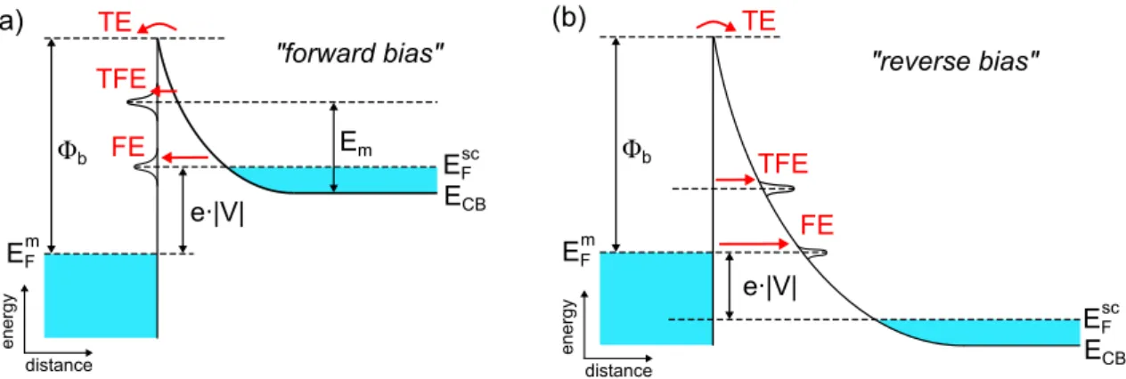
3. Transport measurements on cGNRs on hBN 27 3.1. Theory of Schottky barriers . . . 27
3.1.1. Formation of a Schottky barrier . . . 28
3.1.2. Modifications to Schottky barriers . . . 29
3.1.3. Transport across the Schottky barrier . . . 30
3.2. Sample preparation . . . 34
3.3. Sample characterization by means of AFM . . . 35
3.4. Fabrication of contacts . . . 42
3.5. Transport characterization . . . 47
3.6. Encapsulated cGNR devices . . . 58
3.7. Conclusion and outlook . . . 62
4. Tailoring end states of graphene nanoribbons by magnetic dopants 65 4.1. Theoretical basics . . . 65
4.1.1. Electronic states in GNRs . . . 65
4.1.2. STM imaging with a CO-terminated tip . . . 71
4.1.3. Kondo effect . . . 73
4.2. Sample preparation . . . 78
4.3. First sample characterization . . . 81
4.3.1. End states of 7-aGNRs . . . 81
4.3.2. Variation in the appearance of GNR end states . . . 84
4.3.3. dI/dV spectra on Co atoms on Au(111) . . . 85
4.4. Assembly of Co-GNR-complexes . . . 87
4.5. dI/dV characterization of Co-GNR-complexes . . . 89
4.5.1. Co at middle of armchair edge . . . 89
4.5.2. Co at 3rd position . . . 93
4.5.3. Co at corner position . . . 97
4.5.4. Adding Co to 2nd corner . . . 101
4.5.5. Adding Co to 3rd corner . . . 104
4.5.6. Au atom at corner position . . . 106
4.5.7. DFT calculations . . . 108
4.5.8. Tight-binding calculations . . . 113
4.6. End state broadening . . . 117
4.7. Conclusion and outlook . . . 120
5. Current-induced diffusion 123 5.1. Theoretical basics . . . 124
5.1.1. Electromigration . . . 124
5.1.2. Thermally activated diffusion . . . 126
5.1.3. Kelvin probe force spectroscopy . . . 128
5.2. Experimental procedure . . . 129
5.2.1. Sample preparation . . . 130
5.2.2. Pulsing procedure . . . 130
5.3. Sample characterization . . . 132
5.3.1. Determination of Co adsorption position . . . 133
5.3.2. Lateral manipulation of GNRs with adsorbed Co adatoms . . 135
5.3.3. Exemplary cases . . . 136
5.4. Results and discussion . . . 138
5.4.1. Electromigration . . . 138
5.4.2. One-dimensional diffusion . . . 142
5.4.3. Temperature dependent measurements . . . 147
5.5. Conclusion and Outlook . . . 151
6. Summary 153 A. Fitting of the Kondo temperature 157 B. Measurement setups 159 C. Experimental methods 163 C.1. Fabrication of cGNR devices . . . 163
C.2. Growth of 7-aGNRs on Au(111) . . . 165
C.3. Temperature dependent measurements . . . 166
List of Tables 167
Bibliography 169
After the first isolation of graphene—a single layer of carbon atoms arranged in a honeycomb structure—in 2004 [1], a sort of gold rush started in the research of two-dimensional materials. High mobilities even at room temperature [1], the abil- ity to carry high current densities [2] and excellent thermal conductivity [3] render graphene a suitable material for future device application [4]. Considering also its high transparency [5] and outstanding flexibility [6], the usage of graphene in organic electronics seems promising as well [7]. The emergence of two-dimensional carbon as a possible transistor material comes at the right time since the miniaturization of silicon-based transistor technology is approaching its limits. Therefore, many exper- iments were—and are—conducted to explore the intriguing properties of graphene and graphene-related materials.
The biggest drawback of graphene regarding its electronic applications is its lack of a band gap in its pristine form [1]. This gap is needed to switch on and off the current flow in a device. One way to modify the electronic structure of graphene is to cut it into narrow strips, so-called graphene nanoribbons (GNRs). Thereby the much needed band gap arises due to quantum confinement [8].
There are many ways to fabricate such GNRs. The most promising approach for mass production of high-quality GNRs to this date is chemical synthesis [9]. In recent years, the branch of on-surface synthesis chemistry has made huge advances, enabling the fabrication of a manifold of specifically designed precursor molecules.
By placing them onto a catalytic surface, GNRs with different widths and edge shapes can be tailored [10].
Since the width of the GNR directly influences its band gap [11], it is thus possible to engineer the electronic properties of the GNRs. Hereby, the addition or removal of only a single row of atoms to the GNR width can decide over the existence of a band gap. Furthermore, certain edge shapes may also lead to the emergence of edge magnetism [12, 13].
The formation of different GNRs from precursor molecules on various substrates is an intensely studied topic in surface science [14, 15]. However, little is known about the impact of single adatoms on the electronic properties of the GNRs.
In this work, the electronic properties of GNRs are modified on the atomic scale by adding single Co adatoms to the GNRs. Depending on the exact adatom position, a Kondo-like resonance can be observed in differential conductance spectroscopy.
In order to find applications for GNRs in devices, their transport properties on the
mesoscopic scale are investigated as well [16–18]. Thus, we contacted GNRs with
metal leads and measured their I-V -characteristics.
In an attempt to combine the atomistic and mesoscopic worlds, we investigated how the current flow through GNRs influenced possible doping atoms on the atomic scale.
As an introduction to the topic, some theoretical basics are discussed in chapter 2.
Starting with the physical properties of graphene, the characteristics of GNRs are described. Different methods of GNR fabrication are presented.
Further, the principles of scanning tunneling microscopy and atomic force microscopy are reviewed since both pose important methods to characterize the topography and electronic structure of surfaces with high resolution.
In chapter 3, the deposition of chemically synthesized GNRs on mechanically exfo- liated hexagonal boron nitride (hBN) flakes is described. We observe the formation of ordered GNR domains by means of atomic force microscopy. The GNRs are contacted with different metals and their I-V -characteristics are measured under ambient conditions. Since the realization of reliable contacts is of key importance for the implementation of GNRs in electrical circuits, special focus is put on the formation of Schottky barriers at metal-semiconductor interfaces. Some GNRs are encapsulated with a second hBN flake to protect them from environmental influ- ences, and zero-dimensional end contacts are tested.
Chapter 4 shows how the electronic properties of GNRs can be manipulated by adding single adatoms to the GNR. Here, GNRs are grown under ultra high vac- uum (UHV) conditions in the chamber of a scanning tunneling microscope (STM).
Subsequently, single Co atoms are added to the surface and manipulated under- neath the GNRs with the help of the STM tip. The modifications of the electronic structure of the GNRs upon Co intercalation are probed by differential conductance spectroscopy. For certain intercalation sites, the appearance of a Kondo-like reso- nance can be observed. The experimental results are compared to density functional theory and tight-binding calculations.
The diffusion of Co atoms adsorbed on top of on-surface synthesized GNRs is studied in chapter 5. The GNRs are contacted with an STM tip and current is injected which causes a displacement of the Co adatoms. Remarkably, the Co atoms show a tendency to stay on the GNR during their dislocation, rendering the motion one- dimensional. Temperature dependent measurements are performed to extract the Co diffusion rate.
A summary of the results and a short outlook conclude this thesis.
This chapter will give a brief introduction into the electronic band structure and fabrication of graphene nanoribbons (GNRs) and introduce the basics of scanning probe microscopy. More specific theoretical details will be given at the beginning of the individual chapters.
We begin with a short tight-binding description of graphene. From this starting point, graphene will be confined to one dimension, yielding GNRs. In these narrow strips, quantum confinement leads to quantization of the allowed wave vectors and the development of an electrical band gap. The results are not only dependent on the width of the GNR, but also on the width of the unit cell used to describe the GNR.
To round up this part, different methods of fabricating GNRs are presented and their advantages and disadvantages are discussed.
In the second part, the fundamentals of scanning tunneling and atomic force mi- croscopy are explained. First, an expression for the determination of the tunneling current is derived. Then, the working principle of scanning tunneling spectroscopy is sketched. Last, a short introduction into atomic force microscopy is given and two of its operational modes are introduced.
2.1. Graphene nanoribbons
To understand how the band structure of GNRs evolves form the electronic dis- persion of graphene, some considerations about the lattice and band structure of graphene are presented first. Then, boundary conditions are introduced that occur at the edges of GNRs.
2.1.1. Graphene
Carbon is a very versatile element which constitutes the basis of life with its ability
to form various types of complexes with diverse binding partners in different kinds of
geometries. In its pristine form, it can appear in all kind of dimensionalities. Some
examples are depicted in Fig. 2.1. Carbon atoms can connect to form diamond or
graphite in three dimensions (3D), graphene in 2D, carbon nanotubes (CNTs) and
Figure 2.1.: Allotropes of graphene. Various forms of carbon atom arrangement in different dimensions. From 3D (diamond, graphite) over 2D (graphene) and 1D (carbon nanotubes) to 0D (fullerenes). From [19].
graphene nanoribbons (not depicted here, but discussed in detail later on) in 1D and fullerenes in 0D.
The versatility of carbon is linked to its electronic configuration which is 1s
22s
22p
2in its ground state [20]. However, the formation of hybrid orbitals by mixing s and p orbitals allows carbon to form different types of covalent bonds (single, double and triple) and to develop different structures [21]. Depending on its arrangement, it can hold distinctively different properties. Whereas diamond is electrically insulating, for instance, graphite is conductive.
In graphene, the 2D allotrope of carbon, the carbon atoms are sp
2hybridized and form a planar honeycomb lattice with bonding angles of 120
◦. Three of the four valence electrons develop strong σ bonds with the neighboring atoms. The remain- ing valence electron occupies the p
zorbital which is oriented perpendicular to the graphene plane. Due to the lateral overlap with neighboring p
zorbitals, π bonds are developed. These are delocalized over the graphene plane and account for the conductivity of graphene [22].
The hexagonal lattice of graphene is depicted in Fig. 2.2 (a) and consists of two trigonal sublattices—labeled A (white atoms) and B (black atoms) [20]. The lattice vectors ~a
1= (a
0, 0) and ~a
2= (
12a
0,
√ 3
2
a
0) span a unit cell (shaded in gray) which contains one atom of each sublattice. The distance between two neighboring carbon atoms is a
CC= 1.42 Å and the lattice constant a
0= √
3a
CC= 2.46 Å [23].
The corresponding reciprocal lattice is hexagonal as well. Fig. 2.2 (b) shows the first Brillouin zone (BZ) with the reciprocal lattice vectors ~b
1and ~b
2and the high symmetry points Γ at the center of the BZ, K and K
0at the corners of the BZ and M halfway between them. K and K
0are not equivalent due to the two distinct trigonal sublattices of graphene [22].
The band structure of graphene can be calculated using a tight-binding approach.
This was done for graphite by Wallace already in 1947 [25]. In the simplest form,
only interaction between nearest neighbors is taken into account. In the tight-
biding model, the electrons are considered to be localized at the carbon atoms
(one electron per atom) and to hop from one p
zorbital to the p
zorbital of the
neighboring carbon atom. Next-nearest-neighbor hopping and Coulomb interaction
between the electrons are neglected in the simplest model but can be implemented.
k
xk
yπ*
a
1a
2A B
x
y a
0a
CCb
1b
2M K K'
Γ
(a) (b)
(c) (d)
E/t E
kk
xk
yπ
Figure 2.2.: Lattice and electronic structure of graphene. (a) Honeycomb structure of graphene composed of sublattice atoms A (white circles) and B (black circles) with nearest neighbor distance a
CC. The lattice vectors ~a
1and ~a
2span the unit cell (gray) with the lattice constant a
0. The armchair direction is emphasized by a red line, the zigzag direction by a blue one. (b) First Brillouin zone of graphene with the reciprocal basis vectors ~b
1and ~b
2. The high symmetry points Γ, K, K
0and M are marked. (c) Band structure along the dashed line in (b). The energy is given in units of t. From [24]. (d) 3D energy dispersion of graphene (including next-nearest-neighbor hopping) exhibiting a conical structure at the Dirac points.
From [22].
The derivation of the band structure is not shown here but can be found in detail in Refs. [21, 22, 26]. In short, by writing the eigenfunctions of graphene as a linear combination of Bloch waves, one can solve the Schrödinger equation and obtain the following dispersion relation [21, 22]
E(~k) = ±t
v u u
t 1 + 4 cos
√ 3a
0k
x2
!
cos a
0k
y2
!
+ 4 cos
2a
0k
y2
!
(2.1) Hereby, ~k = (k
x, k
y) is the wave vector and t ≈ 3 eV the nearest-neighbor hopping energy (also referred to as transfer integral or hopping parameter). The correspond- ing band structure can be seen in Fig. 2.2 (c) where the bonding π band (described by the “−” sign in Eq. 2.1 and corresponding to the valence band (VB)) and anti- bonding π
∗band (described by the “+” sign, corresponding to the conduction band (CB)) are depicted along the dashed line in panel (b).
In panel (d), the 3D energy dispersion is depicted as a function of k
xand k
y. Note that for this plot also the next-nearest-neighbor interaction was taken into account which leads to an asymmetry between VB and CB [22]. In the vicinity of the K and K
0points (see zoom-in), the bands have a conical form exhibiting linear dispersion. In the absence of band curvature, the electrons can be described like quasi-relativistic (massless) particles. For this reason, the K and K
0points are also called Dirac points. The energy dispersion close to the Dirac points can be approximated by
E(~k) = ± ~ v
F|~k| (2.2) with the reduced Planck constant ~ and the energy-independent Fermi velocity v
F= 3ta
CC/(2 ~ ) ≈ 10
6m/s.
2.1.2. Lattice and electronic structure of graphene nanoribbons
As evident from the last section, there is no band gap in pristine graphene which would be needed for an application as a transistor material. A gap can be intro- duced by cutting graphene into narrow strips which are called graphene nanoribbons.
Then, quantum confinement can lead to the opening of a band gap [8].
There are two basic shapes of graphene edges [12]. One arises when cutting a graphene sheet along the blue line in Fig. 2.2 (a). Due to the zigzag arrangement of the carbon atoms along this line, the resulting edge is called zigzag edge and the corresponding GNRs are referred to as zigzag GNRs (zGNRs). Analogously, cutting graphene along the red line yields armchair edges and armchair GNRs (aGNRs).
There are also other types of GNR edges but these can be considered as (often pe- riodic) mixtures of armchair and zigzag cusps along the edge.
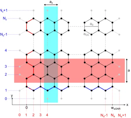
Usually, the width of aGNRs and zGNRs is counted in terms of graphene unit cells,
and therefore in carbon dimers instead of carbon atoms. The corresponding scheme
is explained in Fig. 2.3. Here, the black circles represent the carbon atoms belong-
ing to the GNR. The gray circles indicate the imaginary neighboring atoms of the
a0 aCC
x y
0 1 2 3 4 Na-1 Na Na+1
0 1 2 3 4 Nz
Nz-1 Nz+1
a az
0 waGNR
Figure 2.3.: Lattice structure of GNRs. Armchair and zigzag edge are marked by a red and blue line, respectively. Corresponding dimer lines are counted by the colored markers. The width of the aGNR is indicated. Unit cells of aGNR and zGNR are depicted by shaded rectangles. More details in the text.
graphene lattice. To prevent effects of dangling bonds, the carbon atoms along the GNR edges are considered to be passivated by hydrogen atoms in most theoretical descriptions. In this way, the edge carbon atoms are sp
2hybridized as well and thus host one π electron, just like the carbon sites in the interior
1.
The red line emphasizes an armchair edge that runs along the y-direction. The red labels clarify the counting of the dimer lines and the width of the aGNR is given by
w
aGN R= 1
2 (N
a− 1)a
0(2.3)
with N
abeing the number of carbon dimer lines parallel to the armchair direction and a
0the lattice constant of graphene. The unit cell of the aGNR is displayed as shaded red rectangle. Accordingly, the lattice constant of an aGNR is given by a.
Note that it measures a = √
3a
0and is therefore different from the graphene lattice constant.
1
This is still only an approximation. Although certain aGNRs are predicted to be metallic,
they are found to be semiconducting in experiment. The reason for this is that the hydrogen
termination causes a contraction of the carbon-carbon bond at the edges of these aGNRs that
leads to stronger electron hopping between these edge atoms and thus the opening of a band
gap (see supplemental of Ref. [27]).
V0
x ψA,B λ/2
ψA,B λ/2
waGNR
waGNR *
(a) (b)
Figure 2.4.: Particle-in-a-box model. Cross section of a wave function ψ
A,B(blue) across an aGNR in the ground state with wave length λ. Carbon atoms of the aGNR are displayed as black circles, imaginary next neighbors as light gray circles. The potential V
0outside the aGNR is assumed to be infinitely high (dark gray areas).
(a) and (b) depict the situations for different boundary conditions (see text).
A zigzag edge is highlighted in blue. For zGNRs, the dimer lines run in x-direction and the width is counted as indicated by the blue labels. The zGNR has a unit cell as plotted by the shaded blue rectangle and a lattice constant of a
z= a
0.
In the following, the width of the GNRs will be indicated by adding the number of dimer rows (N
aor N
z) as a prefix to the notation of the GNR. For instance, 7-aGNR refers to an armchair graphene nanoribbon with a width of 7 carbon dimers across the GNR.
Since GNRs share the same lattice with graphene, their band structures are very similar. However, the lateral confinement of the GNRs leads to a quantization of the wave vectors in one direction. In the following, the discretization of the wave vector for aGNRs will be discussed.
In contrast to graphene—which is assumed to be extended infinitely—aGNRs have boundaries. Here, we assume that the aGNRs have a finite size perpendicular to their edges and are infinite along their long axis. These additional constrictions pose special boundary conditions for the wave functions in aGNRs.
The wave vector in k
ydirection (i. e. along the infinitely extended aGNR) is con- tinuous. For the determination of the wave vector across the aGNR, in a first ap- proximation, the wave functions are assumed to vanish on the outer carbon atoms of both armchair edges
2—as displayed in Fig. 2.4 (a). Since the armchair edges host both, A and B sublattice atoms, this means that the wave functions should vanish on both sublattices at both armchair edges [22]:
ψ
A(x = 0) = ψ
B(x = 0) = ψ
A(x = w
aGN R) = ψ
B(x = w
aGN R) = 0 (2.4) Further, one can assume the potential V
0outside the GNR to be infinitely high and treat the GNR states like a particle-in-a-box model. The wave functions ψ
A,Bthen have a wavelength of λ = 2w
aGN R/n with n = 1, 2, ..., N
a. Since wave vector and wave length are related by k = 2π/λ, the quantized wave vector along this direction
2
As will be clarified below, this assumption is not very realistic. Since it is frequently used in
literature, though, it will be discussed here nonetheless.
then reads
k
x= n · π w
aGN R(2.5) Hence, the difference between two allowed wave vectors in k
x-direction is
∆k
x= π w
aGN R= 2π
(N
a− 1)a
0(2.6)
In practice, however, the electrons are not strictly localized at the positions of the carbon atoms but are delocalized due to finite size of the p
zorbital lobes. That means that the wave function is not necessarily zero on the carbon edge atoms. To take this into consideration, the boundary conditions can be modified in such a way that the wave functions vanish at the position of the imaginary neighbors of the edge atoms instead—see Fig. 2.4 (b)—and thus leave a finite amplitude on the edge sites. The width of the aGNR then becomes an effective width
w
aGN R∗= 1
2 (N
a+ 1)a
0(2.7)
and the spacing between two allowed k
xwave vectors reads [28]
∆k
x= π
w
aGN R∗= 2π
(N
a+ 1)a
0(2.8)
Since Eq. 2.8 models the boundary conditions for the wave functions in a more realistic way, only this convention will be used in the following
3.
At this point, it should also be mentioned that the Hamiltonian for the system is sometimes expanded around the K point [22, 29]. In that case, an additional offset for the wave vector appears in Eq. 2.5. This does, however, not affect the spacing
∆k
xbetween allowed k
xvalues.
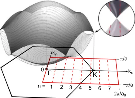
Since the k vectors of GNRs are continuous in one direction (along the GNR) and discrete in the direction perpendicular to that, one obtains a series of parallel lines when plotting the allowed wave vectors for GNRs onto the Brillouin zone of graphene [30, 31]—as is shown in Fig. 2.5. Here, the first BZ of graphene is plotted as a black hexagon. The dashed red lines are the allowed wave vectors of a 7-aGNR which are numbered by the index n from above. The red rectangle marks the first BZ of the 7-aGNR which has a width of 2π/a and a length of 2π/a
0. One can now obtain the band structure of the GNR by projecting the lines of allowed k vectors onto the 3D graphene energy dispersion which is shown above the graphene BZ.
This is indicated in the zoom-in. The GNR bands are therefore line cuts through
3
The choice of the effective aGNR width may appear to be arbitrary. Since the wave function
has to vanish outside the aGNR and its amplitude is defined only at the atom sites in a tight-
binding model, there is a margin on the scale of a few atoms to choose appropriate boundary
conditions. Letting the wave function vanish on the imaginary nearest neighbor site is the most
common method used in literature.
n =
Γ K
1 2 3 4 5 6 7 −π/a
π/a k
yk
x0
2π/a
0Figure 2.5.: First Brillouin zone of 7-aGNR. First BZs of graphene (black
hexagon) and of a 7-aGNR (red rectangle). The allowed wave vectors for the 7-
aGNR are plotted with red dashed lines and numbered by the index n. As depicted
in the inset, the band structure of GNRs is obtained by projecting the GNR wave
vectors onto the 3D graphene energy dispersion that is plotted above the graphene
BZ. See also Fig. 2.6. After [30].
k
xk
yk
xn=1
2 3 4
5 n=1 2
3 4 5
Figure 2.6.: Band structure of 5-aGNR. (a) Electronic dispersion of graphene and lines of allowed k vectors. (b) Cutting lines form (a) projected onto the E − k
xplane. a and t are set to 1. After [32].
the 3D energy dispersion of graphene.
This can be seen even more clearly in Fig. 2.6 from Ref. [32]. Panel (a) shows the energy bands of a 5-aGNR projected onto the 3D graphene energy dispersion. The colored lines are cutting lines of the allowed wave vectors with the graphene disper- sion. Projecting these line cuts onto the E − k
xplane, as shown in panel (b), yields the band structure of 5-aGNRs. t and a are set to unity in this graph.
Interestingly, the bands labeled with n = 4 touch at E = 0 which makes the 5- aGNR metallic. Graphically, the closed gap results from an intersection of one of the allowed k value lines with a Dirac cone of the graphene dispersion.
The spacing ∆k
xof the allowed k lines depends, as shown in Eq. 2.8, on the width of the GNR. The orientation of the lines, on the contrary, is given by the shape of the GNR edges [12]. For zGNRs, the BZ is rotated by 90
◦and for chiral GNRs (GNRs with mixtures of armchair and zigzag cusps) an angle between 0
◦and 90
◦results
4. Whenever a k line cuts a Dirac cone, the corresponding GNR is metallic
5. In the other cases, the GNRs have a band gap.
For aGNRs, it turned out that the resulting band gaps can be grouped into three different families, depending on the aGNR width [11]. According to their number of dimer lines across the aGNR, they are referred to as N
A= 3p, 3p + 1 and 3p + 2 family with p being an integer. The 3p + 2 family is always metallic in the tight- binding description. 3p and 3p + 1 GNRs, on the contrary, have a gap. Due to the increasing effect of quantum confinement with decreasing GNR width, the size of
4
This is also reminiscent of the band structure of CNTs [33–35].
5
At least in the framework of the tight-binding model. Considering effects like electron-electron
interaction can open a band gap in supposedly metallic GNRs.
(a) (b)
Figure 2.7.: Band gaps of aGNRs. Calculation of the size of the band gap with (a) tight-binding and (b) local density approximation. From [11].
the band gap E
gapscales inversely with the GNR width [11]:
E
gap∝ 1
w
GN R(2.9)
Fig. 2.7 shows the band gap of aGNRs in dependence on the aGNR width. The different families are marked by different colors and symbols. In the tight-binding description shown in panel (a), the 3p + 2 family has always a vanishing band gap—
and thus metallic character—and the other two families possess an equally large gap that decreases with aGNR width. Panel (b) shows the band gaps obtained by local density approximation. In that case, all GNRs have a gap, with the 3p + 1 family exhibiting the largest gaps.
Further details on the calculation of the band structure and the determination of the band gaps for the different families can be found in Ref. [32].
Last, the band structure of zGNRs shall be outlined briefly. For zGNRs, the sit- uation is slightly more complicated than for aGNRs because the transversal wave vector does not only depend on the zGNR width but also on the longitudinal wave vector. Details are not discussed here but can be found in Refs. [22, 32].
To give a short summary, tight-binding calculations lead to partially flat bands that
give rise to magnetic order along the zigzag edges. This ordering can be schemati-
cally seen in Fig. 2.8 (b). The color and the size of the circles correspond to the sign
and the magnitude of the local magnetic moment at this position. Note that the
sign of the magnetic moments is the same for all atoms on one sublattice and oppo-
site to the one of atoms on the other sublattice. Thus, all magnetic moments along
one zigzag edge point in the same direction. The magnetic ordering will be further
discussed in chapter 4. At this point, it shall only be stated that the wave functions
are completely localized on one sublattice along the zigzag edge for k
y= π/a
zand
extended across the zGNR for k
y= 2π/(3a
z) [13]. The situation in Fig. 2.8 (b) is an
intermediate state where the magnetic moments are most pronounced at the zigzag
edges but decay towards the zGNR center.
0
ky
π az(a) (b)
Figure 2.8.: Local magnetic moments and band structure of zGNR.
(a) Mean-field Hubbard-model band structure (solid lines) compared with tight- binding band structure (dashed lines). (b) Corresponding distribution of the local magnetic moments. Color and size of the circles indicate sign and magnitude of the magnetic moments. From [36].
According to tight-binding calculations, zGNRs are always metallic. The introduc- tion of Coulomb interaction in the framework of a Hubbard model, however, leads to an opening of a band gap in zGNRs as well. The difference between these two models can be seen in Fig. 2.8 (a). Using a Hubbard model still yields flat bands and therefore magnetic moments at the zGNR edges.
2.1.3. Fabrication of graphene nanoribbons
GNRs with a band gap have great potential in the semiconductor industry, since it allows to turn on and off the current flow in GNR based devices and therefore the use of GNRs as transistor material [4, 12, 37]. There are several ways to obtain GNRs.
GNRs can be fabricated by etching lithographically structured graphene sheets [37], unzipping carbon nanotubes [38, 39] or cutting GNRs out of a graphene sheet with the help of an STM tip [40]. These methods are called top-down approaches because they start with a larger entity which is then reduced to a GNR. The disadvantage of this method is the lack of atomic precision with which the GNR edges are obtained.
This negatively influences the transport properties of the GNRs [41–43].
Another approach is to grow GNRs epitaxially on the stepped surface of SiC. Such GNRs showed ballistic transport [44]. Furthermore, GNRs were grown inside etched trenches in hBN [45]. But again, both of these methods do not yield atomically precise edges.
An alternative path was opened by advances in on-surface chemistry. During the
so-called bottom-up approach, GNRs are formed by fusing small building blocks on
a catalytic metal surface [46, 47]. These surface synthesized GNRs can be fabricated
with atomic precision. Their fabrication process relies on a surface assisted bottom- up assembly of precursor molecules in UHV [46]. By choosing the right precursor molecule, almost all GNR geometries can be realized. Experiments showed the successful on-surface synthesis of aGNRs of different widths [10, 18, 30, 47–51], zGNRs [52], chiral GNRs [53], “chevron”-type GNRs [47] and “cove”-type GNRs (cGNRs) [54]. The shape of the precursor also determines the width of the GNR.
Furthermore, side groups can readily be added to the GNRs [52, 55–57] and doping atoms can be incorporated in the GNR frame [48, 58–61], altering their electronic properties.
A wide range of different catalytic surfaces adds an additional tool to grow GNRs in different shapes and also in specific directions. For instance, placing the precursor molecule DBBA
6on a Au(111) or Ag(111) surface yields 7-aGNRs whereas placing it on Cu(111) gives chiral GNRs [53]. The orientation of the substrate can also be exploited to grow GNRs in a specific direction. The narrow, parallel terraces of the Au(788) surface were used to grow arrays of parallel aGNRs for transistor applica- tion [62, 63].
An advantage of on-surface synthesized GNRs is that no solvents have to be involved in the ribbon growth. Since the process takes place in UHV, the surface stays ex- tremely clean. Additionally, there is an enormous number of precursor molecules, allowing a huge variety of possible GNR shapes.
On the other hand, performing the synthesis in UHV demands sophisticated equip- ment. Additionally, the GNRs are typically grown on metallic substrates which pre- vents their direct electronic characterization, since the GNR states hybridize with the states of the metal substrate. This requires a transfer of the GNRs to an insu- lating substrate which usually involves etchants leaving residues that contaminate the GNRs [16, 18, 64]. There are possibilities to grow GNRs on the semiconducting surfaces of TiO
2[65] and Ge(001) [66], but those GNRs cannot compete with the ones synthesized on metals in terms of edge quality.
To circumvent these problems, one can use solution-processable GNRs [17, 67–69].
They offer a large variety of different shapes as well. Additionally, they are typically longer than their on-surface synthesized counterparts and easy to process. Typically, the synthesized GNR powder is dispersed in a solvent and drop-cast onto an arbitrary surface. This method will be introduced in chapter 3.
6
This molecule will be introduced in chapter 4.
2.2. Scanning Probe Microscopy
This section will give a short introduction into scanning probe microscopy (SPM) which is an important tool to gain insight into the atomic and electronic structure of GNRs and molecules on surfaces. The principles of scanning tunneling microscopy (STM) and atomic force microscopy (AFM) will be introduced. The invention of these two microscopes in the 1980s [70, 71] enabled the direct determination of surface structures in real space and therefore boosted the analysis of surfaces with atomic resolution. Furthermore, it enabled the investigation of (single) adatoms and molecules on surfaces in terms of their geometry and electronic configuration. In SPM, a probe is scanned in close proximity over a sample surface. Whereas STM measures a current between probe and sample, AFM senses the forces between probe and surface. The resulting signals can be transformed into information about the sample topography and electronic structure, as will be explained in the next sections.
2.2.1. Scanning Tunneling Microscopy
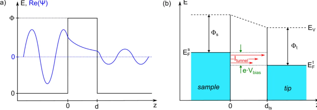
The functionality of STM is based on the quantum mechanical tunneling effect.
The principle of tunneling is sketched for one dimension in Fig. 2.9 (a). An electron wave function ψ can penetrate a barrier with height Φ (much) higher than its own energy. Classically, the barrier would reflect the particle, but the electron can tunnel through it. In the barrier region, the wave function decays with the decay constant κ = √
2m
eΦ/ ~ , where m
edenotes the electron mass.
0
0
0 Φ
d E, Re(Ψ)
z 0 dts z
Itunnel
sample tip
e∙Vbias Φs
Φt EV
EF EFs
t
(a) (b) E
Figure 2.9.: Tunneling at a barrier and energy level alignment in STM. (a)
A wave function ψ (blue) penetrates a tunneling barrier of height Φ. (b) Energy
level alignment in an STM tunneling junction with tip-sample distance d
ts. A bias
voltage V
biasis applied across the junction which causes a tunneling current I
tunnel.
Fermi level and work function of sample (E
Fs, Φ
s) and tip (E
Ft, Φ
t) and vacuum
energy E
Vare indicated.
When bringing together two electrodes very closely, electrons can tunnel through the vacuum gap from one electrode into the other. In STM, one of the electrodes is a conductive probe—called tip—the other one is referred to as sample. When applying a bias voltage V
biasacross the junction, a net tunneling current I
tunnelarises. A scheme for the energy level alignment in this situation can be seen in Fig. 2.9 (b). E
Fsand E
Ftmark the Fermi energies of sample and tip, respectively.
Their respective work functions—i. e. the energy required to remove an electron from the material to the vacuum—are labeled with Φ
sand Φ
t. For reasons of simplicity, it is assumed that Φ
s≈ Φ
t≈ Φ. The vacuum level is denoted with E
Vand tip and sample are separated by a distance d
tsalong the z direction.
To find an explicit expression for the tunneling current, one can follow the description of tunneling introduced by Bardeen [72]. He determined the tunneling current for a metal-insulator-metal junction already in 1961 using a perturbative approach. In this picture, sample and tip are assumed to be separable and their wave functions, ψ
µfor the sample and χ
νfor the tip, can be treated independently. The proximity of sample and tip is considered as a perturbation for the states of the respective other electrode. Thus, the following expression for the tunneling current can be derived:
I
tunnel= 2πe
2~
V
biasX
µ,ν
|M
µν|
2δ(E
µ− E
F)δ(E
ν− E
F) (2.10) with e the charge of an electron, δ(E) the Dirac delta function and M
µνthe tunneling matrix element between states ψ
µfrom the sample and χ
νfrom the tip:
M
µν= ~
22m
Z
Ω
(ψ
µ∇χ
∗ν− χ
∗ν∇ψ
µ) · d ~ S (2.11) Here, the surface integral d ~ S integrates over an area Ω separating tip and sample.
In order to adjust this expression to STM, Tersoff and Hamann [73] evaluated M
µνby modeling the tip as a locally spherical potential well. This potential has a curvature of radius R with its center at position ~ r
0. The model assumes elastic tunneling from occupied to unoccupied states—i. e. conservation of energy—and is valid in the limit of small voltages and temperatures only. By expanding the wave functions of sample and tip and inserting them into Eq. 2.11, the expression obtained for the tunneling current reads
I
tunnel= 32π
3e
2V
biasΦ
2ρ
t(E
F)R
2~ κ
4e
2κRX
µ
|ψ
µ(~ r
0)|
2δ(E
µ− E
F) (2.12) The sum is also referred to as local density of states (LDOS) of the sample at the Fermi level at the position of the tip:
X
µ
|ψ
µ(~ r
0)|
2δ(E
µ− E
F) ≡ ρ
s(E
F, ~ r
0) (2.13)
The decay constant κ in the vacuum region is affected by the applied bias voltage as
κ =
s 2m(Φ − e · V
bias)
~
2(2.14) When measuring at liquid helium temperatures, the limit of small temperature is fulfilled. Sometimes, however, higher bias voltages are used. The Tersoff Hamann model can therefore be extended to finite bias voltages. By assuming that the matrix tunneling element is independent of energy, the equation for the tunneling current reads [74]
I
tunnel= 4πe
~
Z
eV 0ρ
t(E
F− eV + )ρ
s(E
F+ )|M |
2d (2.15) with ρ
s(E) and ρ
t(E) the density of states (DOS) of sample and tip, respectively.
The integral takes into account that all states in the interval between E
Fand E
F+eV contribute to tunneling. The DOS of the tip is assumed to be constant over the energy range of interest and can thus be extracted from the integral. Furthermore, M ∝ ψ(~ r
0) and ρ
s(E, ~ r
0) = |ψ(~ r
0)|
2ρ
s(E). Therefore, Eq. 2.15 yields
I
tunnel∝ ρ
t(E
F)
Z
eV 0ρ
s(E
F+ , ~ r
0) (2.16) From this equation, one can see that the tunneling current is proportional to the integrated local density of states in the sample. That implies that one can map the electronic structure of a sample by means of STM. By considering that the DOS in a metal usually varies smoothly, the changes in electronic structure on a surface can also be related to a change in the geometrical sample topography. Additionally, one always has to keep in mind that the tunneling current is a convolution of tip DOS and sample DOS. Therefore, careful preparation of the STM tip is required in experiments to guarantee a flat DOS of the tip around E
F.
Furthermore, one can see that the tunneling current is proportional to the sample wave function ψ which decays exponentially to the vacuum. Thus, I
tunneldepends critically on the tip-sample separation:
I
tunnel(z) ∝ exp(−2κz) (2.17)
For typical metals (Φ ≈ 5 eV [74]), a change of 1 Å in tip-sample separation changes I
tunnelby roughly one order of magnitude. This fact forms the basis of the high spatial resolution of STM.
The derived theory is based on the assumption of a spherically symmetric tip (with s-wave character). Imaging with a p-wave tip—as in the case of CO tip functionalization—and the correspondingly changed imaging contrast will be dis- cussed in section 4.1.2.
STM has two operating modes to map surfaces. In the constant height mode, the
tip is scanned in x and y direction over a surface whereby the tip height z is kept
unchanged—see Fig. 2.10 (a)—and the tunneling current is recorded. During this,
the tunneling current is measured. Due to its high sensitivity on z, atoms on the surface with diameters of 2–3 Å lead to an increase in I
tunnelby a factor of 100–1000.
The disadvantage of this scan mode is that for highly corrugated surfaces this can lead to a loss of the tunneling signal or—worse—that the tip runs into the sample surface.
z
x,y z
x,y I
tunnelI
tunneld
tsV
biasI
tunnelI
tunneld
tsV
bias(a) (b)
Figure 2.10.: STM operating modes. (a) Constant height mode. The tip is scanned in x and y direction across the sample without changing z. Simultaneously, I
tunnelis measured. The tip-sample distance d
tsvaries. (b) Constant current mode.
The tip is scanned in x and y direction over the sample. z is regulated in order to keep the tunneling current I
tunnelconstant. Images after [75].
To avoid these so-called crashing events, the constant current mode can be used.
Here, z is regulated via a feedback loop in order to maintain a constant tip-sample separation and therefore a constant tunneling current (see Fig. 2.10 (b)). Extension and retraction of the tip give information about the sample topography in that case.
The scanning in x and y direction as well as the control of z are usually done via piezoelectric elements. These elements—typically ceramics in a plate or tube shape—can change their dimensions on the Å scale upon applying a voltage to them.
2.2.2. Scanning Tunneling Spectroscopy
Apart from mapping a surface at a constant voltage (i. e. at a fixed energy), one can also probe the DOS of the sample as a function of energy with an STM. Since the tunneling current is proportional to the integral over the sample LDOS (see Eq. 2.16), its derivative with respect to the current—also called dI/dV or differential conductance—directly reflects the sample LDOS:
dI
dV ∝ ρ
s(E
F+ eV, ~ r
0) (2.18)
To obtain a dI/dV spectrum, the STM tip is spatially fixed at a certain position over the sample and a bias voltage sweep is performed. By measuring the resulting tunneling current, the LDOS can not only be studied at E
F, but at arbitrary energy levels. The corresponding technique is referred to as scanning tunneling spectroscopy (STS). A peculiarity about STS is that it can probe both, empty and occupied states of the sample.
To obtain a better signal-to-noise ratio for the differential conductance spectra, a lock-in amplifier can be employed. In this case, a sinusoidal modulation voltage V
modis added to the bias voltage with a fixed modulation frequency ω. This leads to a periodic modulation of the tunneling current. By Taylor expanding the current as function of the bias voltage and inserting the modulation voltage, one obtains
I (V + V
mod· sin(ωt)) = I(V ) + dI(V )
dV · V
mod· sin(ωt) + ... (2.19) One can thus easily extract the dI/dV signal and hence the LDOS of the sample.
2.2.3. Atomic Force Microscopy
Like in STM, a sharp tip is scanning a sample surface in AFM. In contrast to STM, however, AFM can also map insulating surfaces. Instead of a tunneling current, the forces between tip and sample yield information about the sample topography.
Here, only a brief overview of the basics of AFM and its different operating modes is given. More details can be found in Refs. [74, 76].
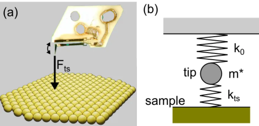
To conduct AFM studies, a sharp tip is mounted to a cantilever and brought in vicinity of the sample surface (see Fig. 2.11 (a)). The interaction between tip and sample then leads to a deflection of the cantilever. Various types of cantilevers are employed in AFM—depending on the type of measurement that is performed.
One distinguishes between static (also called contact) and dynamic (non-contact) operation mode. In static AFM, the tip is dragged over the sample surface. The interaction with the sample leads to a deflection of the cantilever which is then used as the measurement signal. In dynamic AFM, the cantilever is driven to oscillate at or close to its resonance frequency. Due to the tip-sample interaction, the frequency and the amplitude of the cantilever oscillation can change. These quantities are then used as imaging signal in frequency modulation (FM) or amplitude modulation (AM) mode.
To derive a theory for frequency modulated AFM (FM-AFM), the cantilever is modeled as a spring of mass m
∗and stiffness k
0(see Fig. 2.11 (b)). The cantilever is treated as a harmonic oscillator that oscillates at its eigenfrequency
f
0= 1 2π
s k
0m
∗(2.20)
F
ts(a) (b)
k
0m*
k
tstip
sample
Figure 2.11.: Model for tip-sample interaction. (a) AFM tip mounted on a qPlus sensor oscillating over a surface. F
tsresults from interactions between tip and sample. Picture of qPlus from [76]. (b) The cantilever is modeled as a mass m
∗attached to a spring of stiffness k
0. The coupling between tip and sample is taken into account as an additional spring of stiffness k
ts.
For small oscillation amplitudes, the tip-sample force F
tscan be modeled as an addi- tional spring of stiffness k
ts. Then, the oscillation frequency of the cantilever becomes
f = 1 2π
s k
0+ k
tsm
∗(2.21)
By assuming k
tsk
0(i. e. stiff cantilevers) the square root can be Taylor expanded.
Hence, one obtains for the frequency shift
∆f = f − f
0= f
0k
ts2k
0(2.22)
Since ∂F
ts/∂z = −k
ts, it follows
∆f = − f
02k
0∂F
ts∂z (2.23)
By determining the frequency shift of the cantilever oscillation, one thus measures the force gradient perpendicular to the sample surface—i. e. in direction of the can- tilever oscillation.
Various forces can contribute to F
ts. The individual contributions are, e. g., van der Waals force, electrostatic force, magnetic force and chemical forces. Whereas the van der Waals force and the electrostatic force are long-ranged and attractive in nature, the Pauli repulsion (a chemical force) is short-ranged and repulsive. A detailed description of the individual forces can be found in Refs. [74, 76].
FM-AFM is a non-invasive technique. The tip is kept oscillating with a constant amplitude
7in close vicinity to the sample but is not touching the surface. Static
7
Which is established by feedback loops.
AFM, on the other hand, concedes tip-sample contact which can lead to damaging of both, tip and sample.
An intermediate way of operation is the so-called tapping mode [77] (also referred to as intermittent mode). This mode is based on AM-AFM. Here, a cantilever is actuated at a fixed frequency f
drivewhich is close to but different from its resonance frequency f
0. The oscillation amplitudes for the cantilever are typically much larger than in FM-AFM [77]. When the tip starts to make contact with the surface, its oscillation amplitude decreases. A scheme is depicted in Fig. 2.12 (a). The reduction
free amplitude
reduced amplitude
frequency (arb. u.)
ampli tude (ar b. u.)
f
0f
1f
drivecantilever ΔA
sample
diode sensor
(a) (b)
Figure 2.12.: Amplitude modulated AFM. (a) Schematic illustration of the tap- ping mode. A cantilever oscillates over a sample surface. Upon decreasing the tip-sample distance, the tip-sample interaction leads to a decrease of the oscillation amplitude—which is detected with a laser diode and a photo sensor. Image after [78].
(b) The cantilever is kept oscillating with the driving frequency f
drive. When ap- proaching the surface, its resonance curve shifts (from dashed to solid curve) leading to a decrease of the amplitude by ∆A.
of the oscillation amplitude can be registered (for instance) with a laser diode and a position sensitive photo sensor—as indicated in the figure. For this purpose, the cantilever has to be coated with a reflecting material.
The reason for the decrease in oscillation amplitude can be understood from panel (b).
As long as the tip is still far away from the sample, the cantilever has a resonance curve with eigenfrequency f
0(dotted line). When the tip is approached towards the sample, the tip-sample interaction leads to a shift of the resonance frequency of the cantilever to f
1(solid line). Since the driving frequency f
driveis kept fixed during the approach, the oscillation amplitude drops by an amount ∆A. Note that tapping mode is more gentle than contact mode because the tip makes contact with the sample only during a short time of the oscillation cycle.
The choice of AFM operating method depends on the requirement and circum-
stances of the experiment. In this thesis, two different modes are deployed. Tapping
mode is employed to image solution-processed GNRs deposited on hBN flakes. The
cantilevers used for this purpose are made out of coated Si. Furthermore, on-surface
synthesized GNR are characterized in UHV conditions at low temperatures by means
of FM-AFM. In that case, a qPlus sensor is utilized [79]. Apart from its higher stiff-
ness it also allows the simultaneous recording of tunneling currents which is needed
for STM operation.
cGNRs on hBN
In this chapter, solution-processable “cove”-type GNRs (cGNRs) are investigated.
They are dispersed in a solvent and drop-cast onto hexagonal boron nitride (hBN).
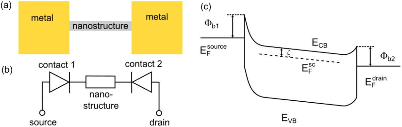
By means of ambient AFM investigations, a formation of ordered cGNR domains on the hBN flakes is found. Using electron beam lithography, the cGNRs are contacted with different metals. Mostly, standard top contacts were applied, but also zero- dimensional end contacts were attempted. The I-V -characteristics of the cGNR devices are dominated by the Schottky behavior of their contacts. By fitting the data with the thermionic field emission model, the height of the Schottky barriers is extracted.
The main results of this chapter are published in [80]. Two master students, Andreas Lex [81] and Christian Kick [82], made considerable contributions in the device fabrication and measurement of the cGNR samples. Some of the images shown in this chapter are similar or identical to images from the publication or their master’s theses.
The samples with zero-dimensional contacts as well as the characterization of further molecules, namely DBOV-TDOP, in the outlook section were done together with the student intern Dhruv Mittal.
For understanding the measured I-V -curves, the principles of Schottky barrier for- mation are of key importance. Therefore, a short theoretical introduction into this topic will be presented at the beginning of this chapter.
3.1. Theory of Schottky barriers
The GNRs investigated in this chapter are of semiconducting nature and they are
contacted by different metals. In general, bringing a metal and a semiconductor into
contact causes a bending of the semiconductor bands and leads to the formation of
a Schottky barrier. This phenomenon is well described in literature and therefore,
the metal-semiconductor junction will be treated only shortly here. More details
can be found, e. g., in Refs. [83–87].
distance
energy
distance
energy
E
VE
FscE
FmE
CBE
VBΦ
mχ
scE
VE
gζ
E
CBE
VBE
FΦ
bΦ
iw
(a) (b)
+ + + + + + ---
Q
mFigure 3.1.: Schottky barrier formation. (a) Energy level alignment for a nor- mal metal (left) and an n-doped semiconductor (right). E
Fmand E
Fscrefer to the Fermi levels of metal and semiconductor, respectively, and Φ
mto the work function of the metal. χ
scis the electron affinity of the semiconductor, E
gits band gap, E
CBthe bottom of the conduction band, E
V Bthe top of the valence band, ζ the distance between E
Fscand E
CBand E
Vthe vacuum level. (b) Upon joining metal and semiconductor, electrons flow into the metal causing a charge Q
mat the metal surface and a depletion layer of width w in the semiconductor. The semiconductor bands bend upwards by an amount Φ
i—called the built-in potential—and a Schottky barrier of height Φ
bemerges at the interface. After [86].
3.1.1. Formation of a Schottky barrier
Fig. 3.1 (a) shows an energy band diagram for a metal on the left hand side and an n-doped semiconductor on the right hand side. Both materials are separated by vacuum and far enough apart so that they do not disturb each other. E
Vrefers to the vacuum level. The metal states are occupied up to the Fermi level of the metal E
Fmand the work function of the metal is denoted by Φ
m.
For the semiconductor, E
CBdenotes the bottom of the conduction band and E
V Bthe top of the valence band. E
grefers to the band gap and E
Fscto the Fermi level of the semiconductor. Its electron affinity (i. e. the distance between bottom of conduction band and vacuum energy) is indicated with χ
sc, and ζ is the distance between Fermi level and conduction band edge. Often, the work function of the metal is larger than the electron affinity of the semiconductor and the two Fermi levels are not aligned.
When bringing metal and semiconductor into contact, as shown in panel (b), the
Fermi levels start to equalize. Charge transfer occurs until a thermal equilibrium is
established. For n-type semiconductors, electrons from the semiconductor flow into
the metal and lead to the accumulation of a charge Q
mat the metal surface. At
the same time, the area in the semiconductor close to the interface gets depleted of free charge carriers and only positively charged ion cores remain. In this so-called depletion region of width w, an electric field evolves due to the charge imbalance that counteracts the flow of electrons from semiconductor to metal. Assuming a homogeneous distribution of the uncompensated donor ions in the depletion region, the electric field in this region will increase linearly with distance from the edge of the depletion region towards the interface and therefore lead to a parabolic band bending. The amount of the band bending is expressed by the built-in potential Φ
i. The resulting potential barrier is referred to as Schottky barrier and has a height of
Φ
b= Φ
m− χ
sc(3.1)
Since Schottky [88] and Mott [89] were the first to describe this relation theoretically, Eq. 3.1 is also known as Schottky-Mott approximation.
Analogously, a Schottky barrier forms for holes when joining a p-type semiconductor and a metal with Φ
m< χ
sc. The corresponding band diagram is not shown here but can be found in the literature [83, 84, 86].
3.1.2. Modifications to Schottky barriers
Experimentally obtained values for Schottky barriers, however, were found to deviate from Eq. 3.1. The discrepancies were explained by the presence of an interface layer of thickness δ between metal and semiconductor [90]. In this layer, interface states form, which are continuously distributed in energy at the semiconductor surface and can be characterized by a neutral level Φ
0that is measured from the top of the valence band of the semiconductor. When these states are occupied up to Φ
0and empty above, the surface is electrically neutral. In general, Fermi level and neutral level do not coincide. This means that a net charge at the semiconductor surface exists—which in turn causes an image charge in the metal surface
1. Thus, a dipole layer develops altering the potential difference at the interface [84, 90]:
Φ
b= γ(Φ
m− χ
sc) + (1 − γ)(E
g− Φ
0) (3.2) with
γ =
ii
+ e
2δD
it(3.3) being a parameter that is indirectly proportional to the density of interface states D
it.
irefers to the permittivity of the interface layer and e to the electron charge.
If there are no interface states, γ = 1 and the Schottky-Mott approximation results from Eq. 3.2. For a very high density of interface states, on the contrary, γ becomes
1