High-mobility graphene in 2D periodic potentials
Dissertation
zur Erlangung des Doktorgrades der Naturwissenschaften (Dr. rer. nat) der Fakultät Physik der Universität Regensburg
vorgelegt von
Andreas Sandner
aus Dollnstein
unter Anleitung von Prof. Dr. Dieter Weiss
September 2017
Das Promotionsgesuch wurde am 03.05.2017 eingereicht.
Das Promotionskolloquium fand am 31.01.2018 statt.
Die Arbeit wurde von Prof. Dr. Dieter Weiss angeleitet.
Prüfungsausschuss: Vorsitzende: Prof. Dr. Milena Grifoni
1. Gutachter: Prof. Dr. Dieter Weiss
2. Gutachter: Prof. Dr. Christian Schüller
weiterer Prüfer: Prof. Dr. Josef Zweck
Contents
List of Figures iv
1 Introduction 1
2 Fundamental properties of graphene 5
2.1 Allotropes of carbon . . . . 5
2.2 Lattice and band structure of graphene . . . . 7
2.3 Dirac fermions and pseudospin . . . . 9
2.4 Electric field effect in graphene . . . . 11
2.5 Transport and scattering mechanisms in graphene . . . . 12
2.5.1 Phonon scattering . . . . 13
2.5.2 Coulomb scattering . . . . 14
2.5.3 Short-range scattering . . . . 16
2.6 Introduction to Quantum Hall effect . . . . 17
2.6.1 Quantum Hall effect in graphene . . . . 19
2.6.2 Quantum Hall ferromagnetism in graphene . . . . 20
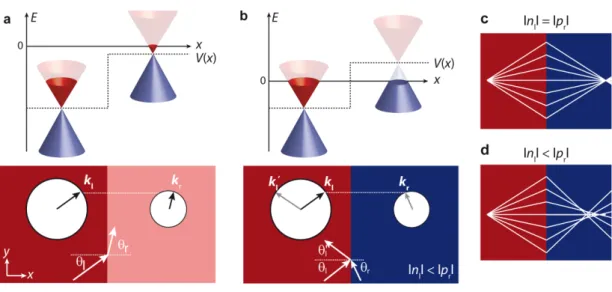
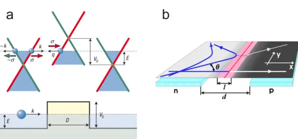
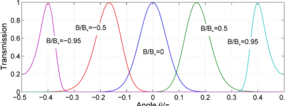
2.7 pn-junctions in graphene . . . . 22
2.7.1 Snell’s law in graphene . . . . 22
2.7.2 Chiral Klein tunneling in graphene . . . . 23
2.7.3 pn-junctions in a magnetic field . . . . 26
3 Graphene-boron nitride heterostructures 29 3.1 Hexagonal boron nitride . . . . 29
3.2 Advantages of hBN-graphene stacks . . . . 30
3.3 Moiré superlattice and Hofstadter butterfly in graphene . . . . 33
Contents iv
4 Commensurability features in lateral superlattices 39
4.1 Weiss oscillations for weak 1D modulation . . . . 39
4.2 Commensurability features for weak 2D modulation . . . . 43
4.3 Strong Modulation: Antidot lattices . . . . 44
5 Sample fabrication and experimental setup 47 5.1 Mechanical exfoliation of graphene and hBN . . . . 47
5.2 Transfer methods and 1D edge contacts . . . . 49
5.3 Thermal annealing of van der Waals heterostructures . . . . 53
5.4 Fabrication of graphene patterned bottom gates . . . . 54
5.5 Measurement setup . . . . 56
6 Ballistic transport in hBN-graphene heterostructures 59 6.1 Improved transport properties of graphene on hBN . . . . 60
6.2 Magnetotransport in high-mobility encapsulated graphene structures 61 6.3 Conclusion . . . . 65
7 Magnetotransport in graphene antidot lattices 67 7.1 Sample fabrication and architecture . . . . 68
7.2 Commensurability peaks in graphene antidot arrays . . . . 69
7.3 Transport characterization of the low density regime . . . . 73
7.4 Discussion of related simulations for graphene antidot lattices . . 74
7.5 Conclusion . . . . 77
8 Interplay between moiré and antidot superlattice potentials 79 8.1 Design and device preparation . . . . 80
8.2 Transport measurements on graphene with moiré and antidot po- tential . . . . 81
8.2.1 Characterization before the antidot etching . . . . 81
8.2.2 Characterization after the antidot patterning . . . . 84
8.3 Conclusion . . . . 89
9 hBN-graphene heterostructures with patterned bottom gates 91 9.1 Device geometry and characteristics . . . . 92
9.2 Magnetotransport experiments with tunable superlattice potential modulation . . . . 94
9.2.1 Experiments with zero back gate voltage . . . . 94
9.2.2 Commensurability peaks for strong modulation in the bipo-
lar regime . . . . 95
9.2.3 Weiss oscillations in a weakly modulated unipolar regime . 96 9.2.4 Temperature dependence of the commensurability oscillations100 9.3 Experiments on further devices . . . . 101 9.4 Conclusion . . . . 102
10 Conclusions and outlook 103
A List of Symbols and Abbreviations 105
B Fabrication details and recipes 107
C Analysis of SdHOs in moiré and antidot superlattices 111
Bibliography 135
List of Figures
2.1 Allotropes of carbon . . . . 6
2.2 Lattice structure of graphene . . . . 8
2.3 Band structure of graphene . . . . 9
2.4 Electric field effect in graphene . . . . 12
2.5 Temperature dependence of resistivity in graphene . . . . 15
2.6 Charged impurity scattering in potassium doped graphene . . . . 16
2.7 Quantum Hall effect in a MOSFET . . . . 17
2.8 Schematics of edge state and broadening of LLs in the QHE . . . 18
2.9 Quantum Hall effect and DOS in graphene . . . . 20
2.10 Symmetry broken integer quantum Hall effect in graphene . . . . 21
2.11 Illustration of Snell’s law in graphene . . . . 24
2.12 Tunneling through a potential barrier in graphene . . . . 25
2.13 pn-junctions in the presence of a magnetic field . . . . 26
2.14 Angular dependence of transmission for different magnetic field values . . . . 27
3.1 Lattice structure of graphene and hBN . . . . 30
3.2 Topography comparison of graphene on hBN and SiO
2. . . . 31
3.3 STEM image of a hBN-graphene heterostructure . . . . 32
3.4 Moiré superlattices in hBN-graphene heterostructures . . . . 34
3.5 Hofstadter’s butterfly in a magnetic field . . . . 36
3.6 Hofstadter butterfly in graphene . . . . 37
4.1 Weiss oscillations in a weakly modulated 2DEG . . . . 40
4.2 Landau band dispersion in a weak periodic potential . . . . 42
4.3 Magnetotransport in a weak, 2D-periodic potential . . . . 43
4.4 Schematic of etched an antidot array . . . . 45
4.5 Magnetotransport in an antidot superlattice . . . . 45
5.1 Exfoliated crystals on a Si/SiO
2substrate . . . . 48
5.2 Schematic of mechanical dry-transfer process . . . . 49
5.3 Transfer setup and stacked hBN-graphene heterostructure . . . . 50
5.4 Crystallographic alignment of hBN-graphene heterostructures . . 52
5.5 Few-layer graphene patterned bottom gate and subsequent device stacking . . . . 55
5.6 AC measurement setup . . . . 57
6.1 Graphene-hBN heterostructure . . . . 60
6.2 Quantum Hall ferromagnetism in graphene . . . . 61
6.3 High-mobility encapsulated graphene structure . . . . 62
6.4 Transverse magnetic focusing in graphene . . . . 64
7.1 Graphene-hBN heterostructure with EBL-patterned antidot lattice 68 7.2 Transport measurements on a hBN-graphene stack with an antidot period of a = 200 nm . . . . 70
7.3 Magnetotransport data taken on a sample with a = 100 nm . . . 72
7.4 Transition between classical and quantum regime at low densities 74 7.5 Comparison of our experiment with a simulation by Power et al. . 75
7.6 Comparison of resistance simulations by Datseris et al. with our experimental results . . . . 76
7.7 Potential contour plot of an antidot system with different kinds of orbits . . . . 76
8.1 Device geometry of a sample with moiré and antidot superlattice . 80 8.2 Device characterization of a graphene moiré superlattice . . . . . 82
8.3 Color plot of the magnetoresistance for a graphene moiré super- lattice before and after antidot patterning . . . . 83
8.4 Magnetotransport experiments in graphene with moiré and antidot superlattice potentials . . . . 85
8.5 Commensurability peaks in a moiré superlattice with an antidot periodicity of a = 250 nm . . . . 87
8.6 Magnetotransport traces in the vicinity of the extra DP . . . . 88
8.7 Magnetotransport experiments at high densities, beyond the sat. Dirac point . . . . 88
9.1 Sample layout, electrostatics and characterization of both gates . 93 9.2 Magnetotransport with V
g=0 V . . . . 95
9.3 Transport experiments in the bipolar regime . . . . 97
9.4 Magnetotransport in the unipolar regime . . . . 99
9.5 Temperature dependence of the commensurability features for weak and strong potential modulation . . . . 100
9.6 Magnetotransport experiments for a device with a graphene PBG
with a = 200 nm and d = 50 nm . . . . 101
Contents viii
C.1 Analysis of the periodicity of the SdHOs for a moiré device with a = 250 nm . . . . 112 C.2 Analysis of the periodicity of the SdHOs for a moiré device with
a = 100 nm . . . . 113
CHAPTER 1
Introduction
Solid state physics has been studied for centuries with focus on electrical, mag- netic or mechanical properties of different materials. During the past decades, the spotlight increasingly moved towards 2D electron systems, exhibiting unique phenomena compared to bulk crystals. Two-dimensional electron gases (2DEGs) are commonly realized in transistor-like semiconductor structures such as MOS- FETs
1, HEMTs
2or quantum wells, and mobilities can be even higher than 10
7cm
2/Vs in AlGaAs/GaAs heterostructures [1]. After all, the 2DEG is not an intrinsic semiconductor property and needs to be formed with gating and modulation-doping techniques in MOSFET and HEMT structures, respectively.
This changed with the first successful isolation of graphene, a monolayer of graphite, by Novoselov and Geim [2]. Graphene is a 2D sheet of carbon atoms, arranged in a honeycomb lattice structure, and features remarkable mechanical and electronic properties. Since its discovery in 2004, graphene has attracted a huge amount of attention and the research field as well as the funding has ex- panded extensively. Many people expect graphene to be a promising material for a variety of possible applications. One characteristic that can be emphasized is graphene’s high intrinsic carrier mobility up to room temperature that would be ideal for transistor devices and could potentially replace the state-of-the-art Si-technology. However, the lack of a band gap in single-layer graphene is a major drawback and hinders the utilization of graphene-based structures in this field. Nevertheless, there might be various applications where the outstanding properties of graphene can be employed: Among others, graphene can be used as an integral part of composite materials [3] (similar to carbon-fiber-reinforced
1metal-oxide-semiconductor field-effect transistor
2high-electron-mobility transistor
1. Introduction
polymer), as an electrode for flexible and transparent displays [4], or as material for supercapacitors [5].
This work focuses on hBN-graphene van der Waals heterostructures and their investigation via transport experiments. For this purpose, we introduced a dry- transfer stacking technique for 2D crystals in our lab and fabricated a huge num- ber of high-quality hBN-graphene hybrid structures. The stacks were analyzed in magnetotransport experiments and/or superposed with an additional 2D su- perlattice potential, subsequently. In this way, we could probe and characterize different commensurability effects stemming from the induced superlattice po- tential and report their influence on transport properties in graphene.
The first sections of this thesis address the fundamental and inherent prop- erties of graphene and the advantages of graphene-hBN heterostructures over prevalently-used graphene on SiO
2substrates. Moreover, the moiré superlattice, resulting from an alignment of graphene and hBN crystals, and the corresponding recursive Hofstadter spectrum will be discussed. Subsequently, commensurabil- ity effects in lateral superlattices - well-known and intensively studied in con- ventional 2DEGs - will be introduced for weak and strong potential modulation in graphene. Then, the various fabrication steps for the samples, including the fundamental stacking procedure and the patterning of local graphene gates, and the experimental setup will be discussed.
Our first goal was to implement the transfer procedure and regularly achieve high-mobility hBN-graphene heterostructures. In chapter 6, we report some of our experiments on graphene on hBN and encapsulated graphene that confirm progress and enhanced sample quality. We routinely observe ballistic transport in our devices with mobilities exceeding 100 000 cm
2/Vs and were able to investigate interaction-driven quantum Hall effects, such as quantum Hall ferromagnetism [6, 7] and the fractional quantum Hall effect [8, 9], in several samples.
The encapsulation of graphene between hBN significantly increases the bulk carrier mobility of graphene, and in chapter 7, we show that any further top- down patterning step does not necessarily degrade the intrinsic quality of the graphene sheet. The high sample quality can be preserved in graphene-based antidot lattices and we successfully probed pronounced commensurability features in antidot arrays with lattice constants down to 50 nm.
Antidot lattices show a nice realization of classical transport in mesoscopic
systems and commensurability features arise from a correspondence of the pat-
terned array with cyclotron orbits [10, 11]. In chapter 8, we study the interplay
between a moiré and an imposed antidot superlattice potential and discuss their
influence on magnetotransport measurements. Commensurability features can be
characterized at various densities and be assigned to the antidot and the moiré
potential. We observe a suppression of the antidot features by approaching the
satellite Dirac points of the moiré potential, accompanied with a distinct super-
position of the classical features with Shubnikov-de Haas oscillations.
In chapter 9, we discuss a new method for imposing lateral superlattice po-
tentials, employing a local few-layer graphene patterned bottom gate [12]. The
patterned graphene gate can be easily implemented in our stacking procedure,
and by tuning the local bottom gate and the global back gate, we can consis-
tently move between the unipolar and bipolar transport regime. In this way, we
are able to report Weiss oscillations [13] in the weakly modulated unipolar regime
and antidot peaks [14] for strong modulation in a bipolar gate configuration.
CHAPTER 2
Fundamental properties of graphene
Graphene is a 2D monolayer of graphite, arranged in a hexagonal honeycomb lat- tice of carbon atoms. It has outstanding material properties such as high stiffness and thermal stability. Additionally, graphene has unique electronic properties such as a linear dispersion relation of the band structure in the vicinity of the Dirac points, followed by a quasi-relativistic description of the charge carriers.
Moreover, there are the electric field effect to tune the charge carrier density and many more interesting features of graphene. Graphene has a high intrinsic mo- bility due to its potentially nearly defect free lattice structure. But graphene on SiO
2is influenced by various scattering mechanisms and the mobility is limited to several thousand cm
2/Vs. As a consequence, one can change the substrate to a more suitable one (e.g. hexagonal boron nitride) or even remove the substrate (suspended graphene), and the mobilities can be enhanced to a few hundred thou- sand cm
2/Vs. After that, the quantum Hall effect and pn-junctions in graphene will be discussed.
2.1 Allotropes of carbon
There are at least two allotropes of carbon that are quite common and universally
known. On the one hand graphite, whose name stems from its ability to leave
marks on paper and other objects (ancient greek: graphein). Graphite is still a
principal component of modern pencils. On the other hand there is diamond,
which has various applications because of its exceptional properties, e.g. as cut-
ting and polishing tools. Although both materials, graphite and diamond, are
consisting of carbon atoms, they have very different characteristics. In diamond
all p-orbitals are bound, forming a sp
3-hybridized crystal without any free elec-
2. Fundamental properties of graphene
Figure 2.1:
Graphene is a 2D basic building block for other sp
2-bonded carbon ma- terials of different dimensions. It can be wrapped up into 0D buckyballs, rolled into 1D nanotubes and stacked into 3D graphite. Fig. from [15].
trons that could be used for charge transfer. So the electronic conductivity in diamond is very weak. In graphite, each carbon atom forms covalent bonds to its three close neighbors, and the additional p
z-orbital is perpendicular to the sp
2- hybrid orbitals and forms a π-bond. The sp
2-hybridization is the reason for the significantly higher conductivity of graphite [16]. Graphite is build up by many 2D carbon sheets, stacked on top of each other, which are bound with relatively weak van der Waals forces to each other.
The first theoretical studies of the bandstructure of 2D carbon layers, named
graphene, were done back in the 1940s by Wallace [17], but it took more than
30 more years to isolate graphene for the first time. Eizenberg and Blakely
managed to get a monolayer of carbon by phase condensation on the surface
of a carbon-doped nickel single crystal. However, the graphene sheet was an
integral layer of a 3D structure. Despite this first breakthrough, the existence
of freestanding, infinitely sized 2D crystals was considered not realistic due to
thermal fluctuations at finite temperatures. This has been the common belief
for several years, because well-established theories showed that the divergent
distribution of thermal fluctuations in low-dimensional crystals can lead to a
displacement of the atoms in the lattice in the order of the magnitude of the
atomic distances [18]. Many different experiments showed exactly this behavior
and so the only way to get graphene was to isolate it as an integral part of 3D
structures with matching lattice constants. Nevertheless, freestanding 2D carbon
2.2. Lattice and band structure of graphene
has been a theoretical system for graphene and its allotropes for many years.
This changed when K. S. Novoselov and A. K. Geim isolated graphene by mechanical exfoliation in 2004 [19]. Since graphite is build up by weakly coupled graphene layers, monolayer graphene is peeled off by chance with “Scotch tape”
and gently rubbed on a Si/SiO
2substrate. From now on, there was the possibility to explore graphene structures on different substrates, as suspended membranes or in suspension. For their significant discovery of graphene, Novoselov and Geim were awarded the Nobel prize in 2010 and started the fast-growing field of graphene research.
As already mentioned, graphene has been a basic concept for the theoret- ical description of different allotropes of carbon. Besides 3D graphite and 2D graphene, there are 0D buckyballs and 1D carbon nanotubes. Buckyballs are spherical carbon molecules that can be characterized by the number of carbon atoms. Carbon nanotubes are one-dimensional, tube-shaped carbon structures with diameters of a few nanometers. One interesting feature of these carbon structures is that all of them have the same hexagonal lattice structure and can be built with graphene. For this, graphene can be wrapped up into buckyballs, rolled into nanotubes and stacked into graphite (see Fig. 2.1). So graphene is the fundamental structure for all the mentioned carbon allotropes.
2.2 Lattice and band structure of graphene
Monolayer graphene consists of a planar, hexagonal lattice, where each carbon atom has three nearest neighbors and four valence electrons. This lattice structure is caused by the sp
2-hybridized orbitals in the x − y-plane that bind with an angle of 120
◦with their neighbors, the so called σ-bond. Only three of the four valence electrons of carbon form a covalent bond. The p
z-orbitals are sticking out of plane, forming the binding π-band and the antibinding π
∗-band. The lateral overlap of the p
z-orbitals leads to a delocalized cloud of electrons, both over and under the carbon lattice plane. Since the delocalized electrons are extended laterally across the x − y-plane, graphene really is a two-dimensional electron gas (2DEG).
The hexagonally arranged carbon atoms, forming the graphene lattice, are shown in Fig. 2.2. The unit cell (dashed lines in Fig. 2.2a) consists of two carbon atoms A and B that give rise to two sublattices with their lattice vectors
~
a
1= a (1, 0) , a ~
2= a − 1 2 ,
√ 3 2
!
, (2.1)
where a = 2.46 Å is the lattice constant. The corresponding reciprocal lattice is
hexagonal, too, featuring the high symmetry points Γ, M, K and K’. Here, the
Dirac points K and K’ in the corners of the graphene Brillouin zone (BZ) are of
particular interest (see Fig. 2.2b). Wallace calculated the energy bands and the
2. Fundamental properties of graphene
Figure 2.2: (a)
Lattice structure of graphene with lattice unit vectors
a~1and
a~2. The unit cell (dashed lines) consists of 2 atoms.
(b)The reciprocal lattice with high symmetry points Γ, K, K’ and M.
(c)Each A Atom (red) is surrounded by 3 B neighbors (blue). The vectors
t~1,
t~2and
t~3connect the A atom with the B atoms of the other sublattice. Fig. adapted from [20].
corresponding bandstructure of graphene back in 1947 [17]. The bandstructure and the essential low-energy dispersion can be calculated employing a “tight- binding approach” [16], where the eigenfunctions of graphene Ψ
i(~k, ~r) (i=1,...,n) can, similar to other crystalline solids, be written as a linear combination of Bloch functions Φ
i0(~k, ~r) and corresponding coefficients C
ii0(~k) [20]:
Ψ
i( ~k, ~r) =
Xni0=1
C
ii0(~k)Φ
i0( ~k, ~r) (2.2) Accordingly, eigenenergies of this system can be obtained with the following ansatz:
E
i(~k) = hΨ
i| H | Ψ
ii hΨ
i| Ψ
ii =
n
P
j,j0=1
H
jj0(~k)C
jj∗0C
jj0n
P
j,j0=1
S
jj0(~k)C
jj∗0C
jj0, (2.3)
with H
jj0(~k) = hΨ
j| H | Ψ
j0i and S
jj0( ~k) = hΨ
j| Ψ
j0i. The equation above needs to be minimized with respect to the coefficient C
jj∗0, resulting in the secular equation [20]:
det[H − ES] = 0 (2.4)
2.3. Dirac fermions and pseudospin
Figure 2.3:
Band structure of graphene. The left figure shows the band structure of single layer graphene. Red lines are
σ-bands and dotted blue lines are π-bands. Theright one is a 3D plot of the electronic energy dispersion in graphene with its cone-like structure. Fig. from [23, 24].
Consequently, the determinant needs to vanish. As a simple first order approx- imation, only the next neighbor interaction will be taken into account. So just H
AA, H
BBand H
ABneed to be evaluated, where A and B are the two atoms of the graphene unit cell. After solving the equations above, the energy dispersion relation of graphene reads as [16]:
E( k ~
x, ~ k
y) = ±γ
0v u u
t
1 + 4 cos
√ 3k
xa 2
!
cos k
ya 2
!
+ 4 cos
2k
ya 2
!
, (2.5) where k
xand k
yare components of the corresponding wavevectors, a = 0.246 nm is the lattice constant and γ
0≈ 3.2 eV is the hopping integral [16, 21]. The resulting band structure is shown in Fig. 2.3.
The energy dispersion of graphene has six points, where valence and conduc- tion band touch, and the non-equivalent points K and K’ are resulting from the two basis atoms in the graphene unit cell. For small energies, in the vicinity of the Dirac points, the energy dispersion is linear in ~k. This linear low-energy relationship gives graphene its unique electronic properties [15, 20, 22].
2.3 Dirac fermions and pseudospin
Looking closely at the Dirac points of graphene, the linear dispersion relation
can be described by two cone-like structures that touch at the K- and K’-points
(see Fig. 2.3). For ideal graphene, the Fermi energy is located exactly at the
position of the charge neutrality point. But in realistic graphene devices, the
Fermi energy can significantly differ from the Dirac energy. Furthermore, the
linear dispersion relation only holds for low energy particles with |E | ≤ 1 eV
and can be well-described by the Dirac equation for massless fermions [25, 26].
2. Fundamental properties of graphene
The Dirac equation describes quantum particles with spin 1/2 (fermions). States with positive and negative energies are conjugated, being described by different components of the same spinor wavefunction [25]. The energy spectrum can be expressed by the following dispersion relation:
E(~k) = ±¯ hv
F|~k|, (2.6)
where the sign indicates if the charge carriers are located in the conduction band (π
∗-band) or in the valence band (π-band). v
F≈ 10
6m/s is the Fermi velocity for carriers in graphene, replacing the speed of light [15, 2, 27]. The low-energy Dirac fermions in the vicinity of the K and K’ points can be characterized by the spectrum of the Dirac-like Hamiltonian:
H ˆ
K= ¯ hv
F0 k
x− ik
yk
x+ ik
y0
!
= ¯ hv
F~ σ · ~k, (2.7) H ˆ
K0= ¯ hv
F0 k
x+ ik
yk
x− ik
y0
!
= ¯ hv
F~ σ
∗· ~k, (2.8) where ~ σ = (σ
x, σ
y) is the 2D vector of the Pauli matrices (~ σ
∗the complex conju- gate) and ~k is the wavevector of the quasiparticles [22]. Here, the Pauli matrices represent the pseudospin that affiliates the charge carriers to one of the sublattices A and B [24]. The pseudospin in graphene is an additional degree of freedom, analogous to the spin symmetry [15, 28]. So all in all, graphene has two different quantum numbers for charge carriers, causing a fourfold degeneracy of states.
The eigenfunctions, as solutions of the Hamilton operators in the vicinity of the Dirac points, can be written as [24, 29]:
Ψ
±,K(~k, ~r) = 1
√ 2
e
−iθ(~k)/2±e
iθ(~k)/2!
e
i~k·
~r, (2.9)
Ψ
±,K0(~k, ~r) = 1
√ 2
e
iθ(~k)/2±e
−iθ(~k)/2!
e
i~k·
~r, (2.10)
where the two-component spinor structure is related to the pseudospin of the
system. Each graphene sublattice is responsible for one of the weakly interacting
valleys of the dispersion and the pseudospin differentiates between the contri-
butions of each sublattice [22, 30]. The projection of the pseudospin on the
momentum ~ p = ¯ h~k is called chirality. Chirality is a conserved quantity and has
important implications on electronic transport in graphene [31, 32]. In particu-
lar a non-trivial Berry phase ins associated with the rotation of the 1/2-pseudo
spinor. A rotation of the angle in momentum space θ( ~k) = arctan (k
y/k
x) by 2π
means a phase shift of the wavefunctions by π, and thus, the spinors will change
sign [29]. This phase shift by π is called Berry phase [33].
2.4. Electric field effect in graphene
2.4 Electric field effect in graphene
The ability to manipulate the electronic properties of a material by applying an external voltage has a huge impact on modern electronic devices. The electric field effect allows to tune the charge carrier density in a semiconductor structure and consequently, to change the electric current through it [19]. This effect is equally important in graphene. One feature that differentiates monolayer graphene from conventional 2DEG structures is the absence of a band gap. The conduction and the valence band touch at the K-points of the energy dispersion. So the Fermi level can be shifted consistently between the valence and the conduction band, corresponding to hole and electron conduction, respectively. In this way, the induced carrier density in graphene can easily exceed 10
12cm
−2[15].
This effect can be experimentally utilized in graphene flakes on a Si/SiO
2wafer. The heavily doped Si wafer acts as a global back gate and the SiO
2layer serves as a dielectric between gate and graphene sheet. Hence, the charge carrier density in the biased graphene flake can be tuned by applying an external po- tential to the Si back gate. Figure 2.4 shows a characteristic gate response of a monolayer graphene flake and schematics of the position of the Fermi level. The electrical resistivity of graphene has a maximum at the Dirac point, where the carrier density has a minimum (charge neutrality point). For undoped graphene the Dirac point should be at V
g= V
cnp= 0, where V
gis the applied back gate voltage and V
cnpthe voltage that needs to be applied to get to the charge neu- trality point. But in most realistic devices, especially in graphene on SiO
2, there is additional intrinsic/ extrinsic doping and V
cnp6= 0.
The high, but finite resistivity peak at the Dirac point can be explained in terms of disorder. This means, in the inevitable presence of disorder, caused by interactions with the substrate or inhomogeneities, regions with electron-rich and hole-rich puddles will arise. These puddles could explain graphene’s anomalous non-zero minimal conductivity at zero average carrier density [34]. The carrier inhomogeneity can be determined by analyzing the broadening of the resistivity peak. Generally, the disorder-induced carrier density fluctuation is a good indica- tor for the sample quality, being as low as δn ≈ 10
10cm
−2in graphene-hexagonal boron nitride (hBN) heterostructures and δn < 10
8cm
−2in suspended graphene [35, 8, 36].
A simple approximation for the back gate induced charge carrier density in graphene on SiO
2can be given with a standard capacitor model. If the lateral dimensions of the graphene flake are much bigger than the thickness of the oxide, the assumption of a plate capacitor is justified. Then, the carrier density on a 300 nm SiO
2substrate can be written as [37]:
n =
0r
de (V
g− V
cnp) ≈ 7.2 · 10
10cm
−2V
−1· (V
g− V
cnp), (2.11)
where
0is the electric constant,
r= 3.9 is the dielectric constant of SiO
2,
2. Fundamental properties of graphene
Figure 2.4:
Electric field effect in graphene. The left figure shows the ambipolar electric field effect in graphene: The Fermi level can be shifted upwards or downwards by applying a positive and a negative gate voltage, respectively. The resistance has a maximum at the Dirac point, where the charge carrier density has a minimum. The right figure depicts a color map of the spatial density variations in a graphene flake for zero average carrier density. The blue regions correspond to holes and the red regions to electrons. Fig. from [15, 34].
d = 300 nm is the thickness of the SiO
2layer and e is the elementary charge.
Using this model, the conductivity of the graphene sheet can be calculated with:
σ = en
sµ =
0r
d µ(V
g− V
cnp) = C
gµ(V
g− V
cnp), (2.12) where C
g=
0r
/d is the gate coupling constant and µ is the charge carrier mobility in the sample. The relation above is one possibility to estimate the mobility of a gated graphene device.
Nevertheless, there are some situations where the plate capacitor model is not valid. In the previous case, the graphene flake is much larger than the thickness of the oxide layer and there is a global gate. Consequently, the electric field lines are parallel to each other and perpendicular to the graphene plane. This is no longer true for smaller lateral dimensions, such as graphene nanoribbons [38, 39]
or locally acting gates [40, 41, 42]. Here, more elaborate simulation techniques for the estimation of the charge carrier density need to be applied.
2.5 Transport and scattering mechanisms in graphene
In contrast to theory, realistic graphene structures always contain defects and
impurities [43, 44]. Additionally, the interaction with the underlying substrate in-
2.5. Transport and scattering mechanisms in graphene
duces edges and ripples [45]. These perturbations strongly influence the electronic properties of graphene and significantly decrease graphene’s quality by acting as scattering centers and introducing spatial inhomogeneities [22]. The mentioned influences to graphene’s transport properties cannot be neglected, and from a theoretical point of view, two different transport regimes can be considered in terms of electron mean free path l
eand length of the graphene channel L.
On the one hand, there is the ballistic transport regime, where l
e> L. Here, charge carriers can run across the graphene sheet without any scattering event.
In this case, transport can be characterized in terms of the Landauer-Büttiker formalism and the conductivity reads as [29]:
σ
L= 4e
2h
L W
∞
X
n=1
T
n, (2.13)
where T
nare the transmission probabilities in all available transport modes. This approach leads to the following expression for the ballistic conductivity as a function of finite carrier density [46]:
σ
L(n
s) = 2e
2√ n
s¯ h (2.14)
Considering evanescent modes in the ballistic regime, this theory leads to a min- imum conductivity at the charge neutrality point [22, 47]:
σ
min= 4e
2πh = 4.92 · 10
−5Ω
−1(2.15)
On the other hand, for l
e< L, carrier experience elastic and inelastic scatter- ing and enter the diffusive transport regime. In this case, the carrier density n
sin graphene is much larger than the inherent impurity density n
iand the system is homogeneous. Accordingly, diffusive transport can be described by the semi- classical Boltzmann theory, where scattering off various impurities is taken into account. At low temperatures the conductivity can be written as a function of the total relaxation time τ [30]:
σ
B= e
2v
Fτ
¯ h
r
n
sπ , (2.16)
where τ depends on the dominant scattering mechanisms in the sample. The most prominent and common ones include Coulomb scattering at charged impu- rities, short-range scattering at defects, and electron-phonon interactions. In the following part, I want to discuss some relevant scattering processes in graphene.
2.5.1 Phonon scattering
At finite temperatures, electron-phonon interactions are a dominant scattering
mechanism in graphene structures. Phonons can be considered as an intrinsic
2. Fundamental properties of graphene
scattering source, limiting the mobility even in absence of extrinsic scattering. In 3D bulk materials, we differentiate between two regimes in terms of temperature.
On the one hand high temperatures T > Θ
D, where the resistivity scales as ρ(T ) ∝ T , and on the other hand ρ(T ) ∝ T
5for T < Θ
D. Since the Debye temperature Θ
D, the temperature scale where all phonon modes are populated, is approximately 2300 K in graphene, we would expect a T
5dependence of the resistivity in our experimental range.
But this is not the case for graphene, where the Fermi surface is substantially smaller than in metals, and only a small fraction of acoustic phonons with mo- menta k
ph< 2k
Fcan scatter with electrons [48]. Thereby phonon energies ¯ hω
phare small in comparison to the Fermi energy of the electrons E
F, and scattering events can be considered as quasi-elastic. This restriction leads to a new temper- ature scale for electron-phonon scattering, the Bloch-Grüneisen temperature:
Θ
BG= 2¯ hv
phk
F/k
B< Θ
D. (2.17) With the sound velocity v
phand the Fermi wave vector k
F= √
n
sπ, Θ
BGcan be determined as
Θ
BG= 54 √
n
sK, (2.18)
where n
sis the carrier density in units of 10
12cm
−2[49].
Again, we need to consider two different regimes, the high and the low tem- perature regime. A related experiment by Efetov et al. can be seen in Fig. 2.5 [48]. For T Θ
BG, we are in the equipartition limit and the Bose-Einstein dis- tribution function for phonons is N
ph≈ k
BT /¯ hω
ph. As a result, there is a linear dependence of the scattering rate on T , and hence, the resistivity ρ is linear in T [49]. On the other hand, there is the low temperature (Bloch-Grüneisen) regime T < Θ
BG, where ¯ hω
ph≈ k
BT . Here, the scattering rate is strongly reduced by the more complicated occupation factor of the phonons. However, in the low temperature limit T Θ
BG, a ρ ∝ T
4relation can be obtained [49].
2.5.2 Coulomb scattering
Coulomb scattering stems from long-range interactions of charge carriers and charged impurities close to the graphene sheet. In this context, charged impu- rities can be trapped ions in the underlying substrate, fabrication residues, or intentionally deposited adatoms. Employing a semiclassical approach using the Boltzmann equation, one can estimate the influence of charged impurity scatter- ing on transport characteristics in graphene. It was predicted that the backscat- tering probability is proportional to √
n
s/n
i, where n
sis the charge carrier density and n
iis the charge impurity density in graphene [50]:
τ
i∝
√ n
s4v
Fn
iπ
3/2(2.19)
2.5. Transport and scattering mechanisms in graphene
Figure 2.5:
Temperature depen- dent part of the resistivity as a func- tion of temperature for different den- sities
n. ∆ρ(T) scales as
T4for low T and crosses over into a linear
Tdependence at higher
T. The inset shows the mobility
µ0as a function on density
n. Fig. from [48].Considering this relation, the conductivity at high carrier densities (n
sn
i) can be written as:
σ
i= Ce
2h
n
sn
i, (2.20)
where C is a dimensionless parameter characterizing the scattering strength [22].
This formula suggests a linear increase of conductivity with charge carrier density for a transport regime mostly influenced by Coulomb scattering. The linear behavior was observed in various experiments on graphene on SiO
2, confirming charged impurities as dominant scattering source [15, 43].
Chen et al. obtained a factor of C ≈ 20 in their experiments, considering
dielectric screening from the substrate and random-phase approximation. They
conducted a systematic study on Coulomb scattering in graphene by depositing
a variable amount of adatoms (potassium) onto a initially clean graphene surface
in ultrahigh vacuum (UHV) [43]. Fig. 2.6a illustrates conductivity versus gate
voltage for a pristine sample and three different potassium doping concentrations
taken at T = 20 K in UHV. A striking result of this experiment is the shift of the
Dirac Point with variation of the adatom concentration. The back gate position
of the charge neutrality point becomes more negative with increasing doping, be-
cause of the shift of the Fermi level induced by the K adatoms. Additionally, the
conductivity as a function of the gate voltage becomes more linear for increasing
impurity concentration, which is is good agreement with equation 2.20 for dom-
inant Coulomb scattering. At the same time, there is a noticeable broadening
of the width of the minimum conductivity region, indicating a reduction of the
sample quality. This decrease in mobility is highlighted in Fig. 2.6b, where the
2. Fundamental properties of graphene
Figure 2.6:
Charged impurity scattering in potassium doped graphene.
(a)The conductivity
σas a function of gate voltage
Vgfor pristine graphene and three different doping concentrations taken at 20 K in UHV. The lines are fits according to equation
2.20and their crossing defines the points of residual conductivity and the gate voltage at minimum conductivity.
(b)Inverse of electron mobility 1/µ
eand hole mobility 1/µ
has function of doping time. Inset: Ratio of
µeto
µhversus doping time. Fig. from [43].
authors found an inverse dependence of the carrier mobility on the density of charged impurities for electrons and holes.
2.5.3 Short-range scattering
Another source of perturbation in graphene are short-range defects such as va- cancies, cracks, step edges and any other topographic defects [51]. Stauber et al. proposed an additional scattering mechanism involving midgap states, which is introduced by these defects. Vacancies lead to a similar k dependence of the relaxation time as charged impurities and the conductivity is roughly linear in n
s[22, 52]:
σ
d= 2e
2πh
n
sn
dln
2( √
πn
sR), (2.21)
where n
dis the defect density and R is the radius of the defect in this model.
This formula is in close analogy to the equation derived for Coulomb scattering
(equation 2.20), with an additional logarithmic dependence on n
s. The almost
linear relation between conductivity and carrier density and the inverse scaling
of mobility with defect density could be proved in experiments in graphene on
SiO
2[44].
2.6. Introduction to Quantum Hall effect
Figure 2.7:
Original QHE exper- iment in the inversion layer of a MOSFET: The graph shows the Hall voltage
UHand the voltage drop be- tween the potential probes
UP Pas a function of gate voltage
Vgat
T= 1.5 K and
B= 18 T. Fig. from [54].
2.6 Introduction to Quantum Hall effect
More than 130 years ago, Edwin Hall interpreted the influence of a magnetic field on a conducting material [53]. The classical Hall effect describes the creation of a potential difference across a conductor, transverse to an electric current, in the presence of a magnetic field. Using this effect, it is possible to determine the density and the sign of of the charge carriers in a bulk material.
Almost exactly 100 years later, Klitzing et al. observed a quantization of the Hall resistance in 2DEG systems [54]. Since its discovery, the so called Quan- tum Hall effect (QHE) has created great interest in the experimental study of the properties of low-dimensional systems [22]. In their experiments at low tem- peratures and high magnetic fields, Klitzing and coworkers found a quantization of the Hall resistivity ρ
xy, corresponding to the value h/N e
2(with N being an integer), and a simultaneous modulation of the longitudinal resistivity ρ
xxas a function of the the carrier density (see Fig. 2.7). The oscillations of the longi- tudinal resistance, the so called Shubnikov-de Haas oscillations (SdHOs), were analyzed precisely and ρ
xxwas going down to zero over the range of each plateau of the quantized Hall resistance. The plateaus can be assigned to integer filling factors ν = n
sh/eB , where n
sis the sheet carrier density [55].
The quantization and oscillation of ρ
xyand ρ
xx, respectively, is universal to
all 2D electron systems. In the following part, I want to introduce the integer
QHE in conventional 2DEGs and discuss the formation of Landau levels (LLs),
the existence of edge states and the role of disorder. For a 2DEG sample with
2. Fundamental properties of graphene
Figure 2.8:
Schematics of edge states and broadening of LLs in the QHE:
(a)A finite 2DEG under a perpendicular magnetic field B. A large area is quantized at n =1 while, due to potential difference, a small n = 2 LL is formed in the middle of the sample.
Grey circles with arrows indicate the cyclotron motion.
(b)Formation of edge channels in the LLs. (c) Density of states with broadened LLs. Fig. from [55].
finite dimensions, exposed to a magnetic field B (see Fig. 2.8a), we can approach the energy spectrum and the quantization of the LLs by solving the Schrödinger equation of a single particle [56]:
1
2m (~ p + e ~ A(~ r))
2+ V (z)
Ψ(~ r) = EΨ(~ r), (2.22) where A ~ is the vector potential of the magnetic field B ~ and V (z) is the quantized potential along the ˆ z-direction. The solution of the Schrödinger equation gives the quantized, equidistant Landau levels:
E
n= ¯ hω
c(n + 1
2 ) with n = 0, 1, 2, 3, ..., (2.23) where ω
cis the cyclotron frequency of the electrons. For the integer Quantum Hall effect, the transverse conductivity can be written as:
σ
xy= ν e
2h = f n e
2h , (2.24)
2.6. Introduction to Quantum Hall effect
where n is the number of filled LLs and f = 2 is the spin degeneracy in the 2DEG system.
The quantized Hall resistance and the SdHOs can be explained with 1D con- ducting edge channels, originating from the LL bending. Fig 2.8b shows the LLs and the formation of channels along the edges of the sample. Considering the edge boundary condition Ψ(x = 0, W ) = 0 and the approximately parabolic band structure of the band edges in momentum space, the energy of the LLs increases as they approach the edges [55]. The only states that carry the current are the edge states at the Fermi level E
F. Filling factor ν = N implies, there are N conducting edge states, coinciding with a quantized Hall resistance ρ
xy= h/N e
2[57]. The currents on each edge are running in opposite directions, due to the cyclotron motion in the perpendicular magnetic field. Thus, the only source of backscattering would be electrons going from one edge to the other. In this way, the onset of interaction between the two sets of edge states leads to deviations from exact quantization and eventually to a breakdown of the quantum Hall regime [57]. Otherwise, the suppression of backscattering in the QHE regime leads to a vanishing ρ
xxand induces dissipationless transport.
Nevertheless, the model of conducting edge channels does not explain the Fermi level pinning between the LLs. Here, we need to consider vacancies and impurities that cause the broadening of the density of states (DOS) and the formation of localized states at its slopes (see Fig. 2.8c). The charge carriers cannot scatter into the localized states and the Fermi energy gets pinned, resulting in the experimental observation of QHE plateaus with finite width [22].
2.6.1 Quantum Hall effect in graphene
Since graphene is a 2D material, one of the first and most important experimental results was the observation of the quantum Hall effect (see Fig. 2.9) [2, 27]. Con- sidering its unique properties regarding lattice and band structure, the quantum Hall effect in graphene is significantly different than in conventional 2DEG struc- tures. Graphene’s sublattice symmetry adds an additional degree of freedom, so the charge carriers have a fourfold degeneracy (two spin, two pseudospin). Thus, the resulting energies of the LLs are no longer equidistant, but have a square root dependence on the magnetic field B:
E
n= ±
q2e¯ hv
F2|n| B with |n| = 0, 1, 2, 3, ... (2.25)
Here, n > 0 and n < 0 are for electron-like and hole-like Landau levels, respec-
tively. This energy spectrum results in an unconventional, half-integer sequence
of energy levels with the presence of a distinctive LL at E
n= 0 [58, 59]. The
n = 0 LL is formed with degenerate electron and hole states, leading to a half-
integer shift in the number of flux quanta needed to fill an integer number of LLs
(see Fig. 2.9) [55].
2. Fundamental properties of graphene
Figure 2.9:
Quantum Hall effect and density of states in graphene.
(a)Hall conduc- tivity
σxyand longitudinal resistivity
ρxxas a function of carrier density
nat
B= 14 T and
T= 4 K in monolayer graphene. The minima of the SdHOs follow the half-integer plateaus in
σxy.
(b)DOS of graphene with the zero-energy LL and
(c)DOS of a conventional 2DEG with equidistant LLs. Fig. from [2].
As a consequence of the half-integer quantization of the energy levels, the quantum Hall conductivity is shifted with respect to the standard QHE sequence by 1/2 and reads as follows:
σ
xy= ν e
2h = 4e
2h (n + 1/2). (2.26)
Since the energy difference between the first and the second LL ∆E =
q2e¯ hv
F2B ≈ 200 meV (at B = 30 T) is significantly higher than the thermal energy at room temperature, the quantum Hall effect in graphene can even be observed at high temperatures (and high magnetic fields) [60].
2.6.2 Quantum Hall ferromagnetism in graphene
Two different kinds of massless Dirac particles, centered on the two inequivalent
valleys, can be described in a low-energy effective theory of graphene. In high
magnetic fields, the valley and electron spin degeneracy lead to the anomalous
graphene quantum Hall sequence (Equation 2.17). Many different broken sym-
metry states can appear in electronic systems with multiple degenerate degrees of
freedom [61]. Strong Coulomb interactions and a fourfold spin-valley degeneracy
cause a SU(4) isospin symmetry in graphene Landau levels [62, 6]. At partial
filling of these LLs, exchange interactions can break this symmetry and polarize
2.6. Introduction to Quantum Hall effect
Figure 2.10: