Transport and noise properties of AlGaN/GaN heterostructures for high-frequency applications
104
0
0
Volltext
(2)(3)
(4)
(5)
(6)
(7)
(8)
(9)
(10)
(11)
(12)
(13)
(14)
(15)
(16)
(17)
(18)
(19)
(20)
(21)
(22)
(23)
(24)
(25)
(26)
(27)
(28)
(29)
(30)
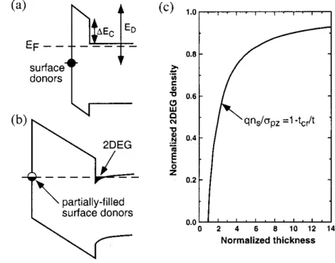
Abbildung
![Figure 1.2. Experimental values of the effective mass measured for different 2DEG density [36-41]](https://thumb-eu.123doks.com/thumbv2/1library_info/3644776.1502986/17.892.165.825.320.1059/figure-experimental-values-effective-mass-measured-different-density.webp)
![Figure 3.1. Schematic diagram of a continuously operating 4 He evaporation cryostat with a separate 4 He pot [120]](https://thumb-eu.123doks.com/thumbv2/1library_info/3644776.1502986/33.892.521.791.181.401/figure-schematic-diagram-continuously-operating-evaporation-cryostat-separate.webp)
![Figure 3.2. Sketch of a 3 He cryostat with charcoal absorption pump [120].](https://thumb-eu.123doks.com/thumbv2/1library_info/3644776.1502986/34.892.250.713.120.473/figure-sketch-cryostat-charcoal-absorption-pump.webp)
+7


ÄHNLICHE DOKUMENTE
A relative permittivity value of about 700 was obtained for pure KNN at room temperature which is high compared to what has been previously reported in the literature 2,3..
In this study the radiation shielding properties of three different types of steel, namely stainless steel (SS), carbon steel (CS) and speed steel (VS), have been determined and
Starting materials for the preparation of SmRhIn were sublimed dendritic pieces of samarium (Johnson Matthey), rhodium powder (Degussa-H¨uls, 200 mesh), and indium tear drops
Bi-modal grain distribution is observed in the samples while the average grain size decreases with co-doping due to grain growth inhibition by pinning of the grain boundary
These features of the AlZn-Ti3 master alloy allow to decrease a detrimental overheating of the Zn-Al alloys melt, which avoids melt oxidation, reducing the costs of energy
At the atomic scale, magnetic anisotropy originates from anisotropy in the orbital angular momentum and the spin-orbit coupling that connects the spin moment of a magnetic atom to
In addition, we have investigated the anisotropy of the normal-state resistivity of a number of superconducting Bi-2201 and Bii.7Pbo.3Sr2CaCu208+8,(Pb-doped Bi-2212) single
In this study, the experimental parameters of longer diffu- sion time and a higher injection pressure of helium, applying the multi-pulse method, and cycling the confining pressure
