Effect of Lithium doping on the optical properties of monolayer MoS
2Nihit Saigal
1,a, Isabelle Wielert
1, Davor ˇ Capeta
2, Nataˇsa Vujiˇ ci´ c
2, Boris V. Senkovskiy
1
, Martin Hell
1, Marko Kralj
2, and Alexander Gr¨ uneis
11
II. Physikalisches Institut, Universit¨ at zu K¨ oln, Z¨ ulpicher Strasse 77, 50937 K¨ oln, Germany
2
Center for Excellence for Advanced Materials and Sensing Devices, Institute of Physics, Bijeniˇ cka 46, 10000 Zagreb,
Croatia
The effect of Lithium atoms evaporation on the surface of monolayer MoS
2grown on SiO
2/Si substrate is studied using ultra high vacuum (UHV ∼ 10
−11mbar) Raman and circularly polarized photoluminescence spectroscopies, at low Lithium coverage (up to ∼0.17 monolayer). With increasing Li doping, the dominant E
12gand A
1gRaman modes of MoS
2shift in energy and broaden. Additionally, non zone-center phonon modes become Raman active. This regards in particular to double resonance Raman scattering processes, involving longitudinal acoustic (LA) phonon modes at the M and K points of the Brillouin zone of MoS
2and defects. It is also accompanied by significant decrease in the overall intensity and the degree of circular polarization of the photoluminescence spectrum. The observed changes in the optical spectra are understood as a result of electron doping by Lithium atoms and disorder-activated intervalley scattering of electrons and holes in the electronic band structure of mono- layer MoS
2.
a) Electronic mail : nihsai7795@gmail.com
Monolayer (ML) Molybdenum Disulphide (MoS
2) is one of the most extensively studied members of the family of layered two dimensional (2D) materials. It shows several inter- esting physical phenomena such as, a direct bandgap leading to efficient photoluminescence (PL)
1,2, many body physical effects eg. observation of trions
3and biexcitons
4, spin-valley coupling
5,6, exciton-phonon coupling
7,8etc. State-of-the-art devices like field effect transis- tors, solar cells, light emitting diodes etc. have been demonstrated based on these properties of MoS
2.
9Optical techniques like PL, Raman, reflectance and absorption spectroscopies have played a major role in MoS
2related research.
10However, the optical spectrum of this mate- rial is strongly affected by the presence of dopants and defects in the lattice. For instance, excitons bind to mono and bi- Sulfur vacancy defects in the ML MoS
2lattice and lead to additional features in the PL spectrum apart from the nearly free exciton transition.
11,12Raman spectrum of ML MoS
2is strongly affected by the presence of structural defects and additional phonon modes become Raman active in the disordered crystal.
13The peak energy and intensity of PL spectrum in ML MoS
2can be tuned by chemical doping.
14Thus, it is important to systematically study the effect of dopants and disorder on the optical proper- ties of ML MoS
2.
Previously, several strategies have been used for doping MoS
2using different
natured dopants, that include chemical treatment
14–16, substitutional doping
17,18,
surface evaporation of dopants
19,20and gating in a transistor geometry
3,21. It
has been shown both theoretically and experimentally that surface adsorption
of alkali metal atoms like Li, K, Cs etc. is an efficient way to reach very high lev-
els of n-type doping (∼10
14cm
−2electron density) in 2D materials.
22,23In bulk
or in epitaxially grown layers (in epitaxial case even in ML limit) deposition
of alkali metal atoms leads to ordered (intercalated) structures and possibility
to precisely determine and correspondingly control charge transfer per added
atom.
24–26,28On the other hand, for the adsorption of alkali metals or any other
atoms or molecules on ML MoS
2(or other 2D materials) transferred or directly
grown on an amorphous SiO
2support, such quantification is far from straightfor-
ward, notably because intercalation or stable adsorption of well-defined ordered
structure does not occur.
18Despite this difficulty, the investigation of atomic
and molecular adsorption on single or few-layer 2D materials on a dielectric
amorphous support such as SiO
2, is of great importance with respect to possible
applications, for example in sensors based on field effect transistors or in related devices for detection of changes in the optical response.
19,29Also, investigation of the optical spectra of doped ML MoS
2using circularly polarized light is im- portant for design of valleytronic devices.
5,6Another interesting aspect of this material is the existence of phases which differ in their structural and electronic properties. In 2H phase of MoS
2, Mo atoms have trigonal pris- matic coordination and the crystal is semiconducting while in the 1T phase, Mo atoms have octahedral coordination and the crystal is metallic.
30,311T MoS
2had been widely studied in bulk form due to its application as anode material in Lithium (Li) ion batteries.
31Recently, it has gained renewed interest due to its strong non-linear optical effects
20, application in low resistance transparent contacts fabrication
29, theoretical prediction of a small bandgap opening in the distorted (1T
0) form etc.
32Several strategies have been used to obtain the 1T phase of MoS
2from its naturally occurring 2H phase, such as Li atom intercalation
20,31, elec- tron beam irradiation
25and electron transfer from a metallic substrate
33etc. Although, Li ion intercalation in 2H-MoS
2has been extensively investigated for Li-ion batteries
26,31and chemically/electrochemically exfoliated preparation of single- layer MoS
2nanosheets
15,29, the structural evolution of MoS
2, especially the in- termediate phases such as 1T-MoS
2and the occupancy of the Li atoms in it, is still not clear.
27In this letter, we discuss our investigation of the effect of in-situ evaporation of Li atoms on the surface of ML MoS
2on SiO
2/Si substrate under ultra high vacuum (UHV) (10
−11mbar) conditions using micro-Raman and circularly polarized micro-PL spectroscopies at low tem- peratures (∼6K). We observe that Li doping causes shifts and line-broadening of the domi- nant Raman modes of MoS
2and appearance of new Raman modes. Also, the intensity and circular polarization of PL spectrum of MoS
2are affected by Li doping. Our analysis of the Raman and PL spectra evolution with Li doping, indicates that the observed changes may arise from electron doping and disorder in the ML MoS
2lattice caused by Li atoms. Here, we would like to comment that such a behavior has not been obtained in case of potassium doping in ML MoS
2.(see supplementary material)
Monolayer 2H MoS
2films were grown in a homemade chemical vapor deposition (CVD)
system from MoO
3and S precursors. Sulfur vapor was produced by heating 50-100 mg
of Sulfur to 140
oC by a separate heater in front of the main furnace. Growth substrate,
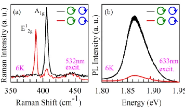
FIG. 1. Circular polarization resolved (a) Raman and (b) PL spectrum of ML MoS2. Green and blue circular arrows denote the excitation polarization of laser and detection polarization for the backscattered Raman and PL signals of the sample respectively.
285 nm SiO
2on highly doped Si, was placed in center of the furnace and heated to 750
oC during growth which typically lasted for 10 minutes. After growth, the substrate was cooled in furnace to 200
oC in Ar stream before removal. The samples were mounted on sample holders and moved inside a home built UHV system
35,36. They were initially annealed in the preparation chamber at 200-250
oC under UHV for 2-3 hours to get rid of the surface residues and subsequently transferred to the analysis chamber equipped with a liquid He cryostat and an optical window for spectroscopic studies. The Li evaporation was done in steps inside the preparation chamber using high purity SAES Li getters with samples kept at room temperature. A quartz microbalance was used to estimate the thickness of deposited Li. 100 s of Li evaporation corresponds to ∼0.13 ML coverage of Li. After each evaporation step the sample was put back in the analysis chamber and was given sufficient time to cool down before doing measurements. Samples were excited using either 532 nm or 633 nm laser beams. A combination of linear polarizers and quarter wave plate along with a commercial Renishaw spectrometer were used for circular polarization resolved Raman and PL spectroscopy (see supplementary material). The spectral and spa- tial resolution of the setup were ∼0.5 cm
−1and ∼5 µm respectively.
Figures 1(a) and (b) show the results of circularly polarized Raman and PL measurements respectively. The green and blue circular arrows indicate the polarization of the excitation laser beam and that of the detected Raman or PL signal respectively. Clockwise rotation is for right circular polarization (RCP) and anti-clockwise for left circular polarization (LCP).
Figure 1(b) shows the helicity dependence of the two main Raman modes. First note that
FIG. 2. (a)-(d) Experimental spectra (black) and Lorentzian fits (red) for the Raman peaks around the E12g (blue)and A1g (pink)Raman modes of ML MoS2 for different Li exposure times.
(e)-(h) Experimental Raman spectra and Lorentzian fits for the new Raman modes for different Li exposure timesincluding Raman modes due to LA(K) (dark grey) and LA(M) (orange) phonons. Dark green peaks in panels (a) - (h) denote the individual Lorentzian peaks due to the other identified Raman modes (see supplementary material). (i) Peak energy and (j) linewidth of the E12g and A1g Raman modes as a function of Li exposure time. (k) Ratio of the intensity of Raman modes due to LA(K) and LA(M) phonons and that of the E12g mode, as a function of Li exposure time.
the energy difference between the two modes is ∼18 cm
−1which confirms the
ML quality of our sample.
37We also observe that, while the A
1gmode is dominant when
the helicity of the detected Raman signal matches with that of the excitation laser, E
12gmode is active only for the detection of opposite helicity. This helicity dependence comes
from the symmetry properties of these phonon modes.
38These results are completely in
line with previous studies
38which prove the feasibility of our setup and the good quality
of our samples. The time reversal symmetry and absence of inversion symmetry together
with a large spin-orbit (s-o) coupling in ML MoS
2leads to optical spin-valley selection rules
such that in the absence of inter-valley scattering (IVS) processes, a sample excited using a
circularly polarized light with energy in resonance with an exciton transition, should show
PL with the same helicity as the excitation source.
5,6Thus, a highly circularly polarized PL
signal as shown in Fig. 1(b) is again an indication of the good quality of our pristine ML MoS
2samples.(supplementary material)
After certifying the good quality of our sample, we proceeded to stepwise evaporate Li atoms
on the surface of MoS
2, in-situ without exposure to air. After each step, the Raman and
circularly polarized PL spectrum of the sample were obtained. Note that all measurements
were done at low temperature (6K on the sample holder) to eliminate removal of Li atoms
caused by laser heating. Low temperature is also relevant to make the Li atoms immobile,
since at room temperature the charge transfer from Li atoms to MoS
2may vary due to
mobility and/or loss of Li atoms. Figures 2(a) - (h) show the experimental spectra and
Lorentzian fits to Raman spectrum for different Li exposure times. They show that on Li
exposure, apart from E
12gand A
1gRaman modes, a number of new phonon modes become
Raman active. These modes were previously observed in ion-bombarded ML MoS
2.
13Based
on previous studies, we can attribute majority of these modes to be due to phonons at the
M and K points of Brillouin zone (BZ), which become Raman active in the presence of
disorder in the MoS
2lattice (see supplementary material).
13,39Figures 2(i) and (j) respec-
tively show the changes in peak energy and linewidth of the E
12gand A
1gRaman modes as
a function of Li exposure time. The A
1gmode shows an initial redshift in energy and an
increase in linewidth after 30 s of Li exposure. In subsequent Li exposure steps, it blueshifts
and keeps broadening. The E
12gmode shows a small blueshift in the first Li exposure step
and redshift in subsequent exposures. The A
1gRaman mode in MoS
2is sensitive to the
electron density and a redshift and broadening of this mode is an indication of electron
doping of ML MoS
2by Li atoms.
21We estimate the electron density in MoS
2at this stage
to be ∼0.3×10
13cm
−2.
21However, the subsequent blueshift of this mode with increasing Li
exposure cannot be explained by electron doping. This may likely result form the breaking
of translational symmetry of phonons due to disorder in the MoS
2lattice and their resultant
spatial confinement.
13,40Some of the new Raman modes (Fig. 2(e) - (h)) can be identified
as due to double resonance Raman scattering (DRR) processes involving the LA(M ) and
LA(K) phonons and defects in the ML MoS
2lattice.
13,39The Raman modes due to LA(K )
and LA(M ) phonons have a dispersion of -24.5 cm
−1/eV and -10.5 cm
−1/eV respectively.
39We fixed the peak positions of these modes for 532 nm (2.33 eV) excitation and fitted our
data using Lorentzian lineshape functions. In Fig. 2(k), we plot the ratio of the intensity of
the Raman modes due to LA(K ) and LA(M ) phonons to that of the E
12gRaman mode. This
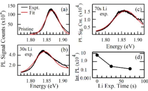
FIG. 3. (a)-(c) Experimental data (black) and Gaussian fits (red) for the circularly polarized PL spectrum (excitation and detection of right circular polarization) of ML MoS2 for different Li exposure times. (d) The integrated PL intensity as a function of the Li exposure time.
ratio quantifies the disorder in the MoS
2lattice.
13An increase in this ratio with increasing Li exposure time shows that disorder in MoS
2lattice increases with increasing Li doping. As we mentioned above, Li doping can lead to the 2H to 1T phase transition in MoS
2for high Li coverage (∼2 ML of Li).
15,24This transition is driven by the electron transfer from the Li atoms to MoS
2, which results in stabilization of the 1T phase relative to the 2H phase due to the absence of a bandgap in the former.
24,30,31Structurally, the transition involves a rear- rangement of atoms in MoS
2which can cause lattice distortions and grain boundaries.
25,31Thus, the tendency to undergo the phase transition from 2H to 1T form with Li doping could be responsible for the observed structural disorder in ML MoS
2.
15,24Figures 3(a) - (c) show the experimental data and Gaussian fits for the circularly polarized
PL of ML MoS
2for different Li exposure times. Note that we do not fit the data for the sam-
ple with 130 s of Li exposure because its PL has almost entirely vanished and the spectrum
is dominated by background of the Raman signal. Also, the fits are not ideal because apart
from the exciton transition, the PL may have contribution from an unresolved trion related
transition.
3,8,14After the first 30 s of Li exposure, PL peak shows a redshift due to electron
doping from Li atoms.
3After 70 s of Li exposure, it blueshifts. Such blueshift of the PL
spectrum of ML MoS
2was also seen earlier in disordered samples.
41Figures 3(d) shows the
plot of integrated PL intensity with increasing Li exposure. We observe that the PL decays
by more than three orders of magnitude after 70 s of Li exposure. The observed decay
of PL intensity originates from different factors dominating at different stages
of Li doping. Initially, electron doping due to charge transfer from Li atoms re-
sults in trion formation (also evident from the redshift of the PL spectrum) and consequent decrease in the radiative recombination of excitons.
3,14With further increase in Li doping, structural disorder dominates as indicated by the changes in the Raman spectrum and also blueshift of PL spectrum. Structural defects in MoS
2can serve as sites for excitons to bind and decay non-radiatively.
16Also, disorder promotes IVS of electrons and holes to neighboring valleys from where they can possibly find paths for non-radiative decay.
39Finally, with further in- crease in Li doping, the change in the band structure around the K-point due to the 2H to 1T phase transition leads to complete vanishing of the PL.
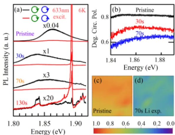
15,34Figure 4(a) shows the evolution of the circularly polarized PL with Li doping. As we dis- cussed earlier, the circular polarization of the PL spectrum is due to spin-valley optical selection rules. The degree of circular polarization is defined as
ρ = I(RCP ) − I(LCP )
I(RCP ) + I(LCP ) (1) where I(RCP)/I(LCP) denote the intensities of the RCP/LCP PL signals.
6ρ is a measure of valley polarization (VP) in ML MoS
2.
6Figure 4(b) shows a plot of ρ around the PL peak en- ergies, for different Li exposure times. It shows that ρ decreases with increasing Li exposure.
To make sure that we have not been probing a defective region of the sample by chance, we measured 30×30 µm spatial maps of ρ in a typical region of the sample. Figures 4(c) and (d) show the maps for the pristine and 70 s Li exposed MoS
2sample respectively. The maps show that for pristine sample ρ is between 0.8-0.9 while after 70 s Li exposure, it decreases to 0.5-0.6.
The observed decay in the degree of circular polarization of PL (which is a measure of
VP) can result from two main mechanisms. One is electron doping from Li atoms which
may lead to increase in the electron-hole exchange interaction resulting in decrease in VP or
valley depolarization.
6However, one does not observe a significant decrease in PL circular
polarization for Potassium doping in ML MoS
2.(see supplementary material) The second
mechanism is IVS processes. IVS in ML MoS
2requires a simultaneous spin flip and a large
change (∼K) in the crystal momentum of the excited carriers.
6Following resonant excita-
tion of electron-hole pairs in ML MoS
2, the electrons can undergo a fast spin flip due to
very small (∼3 meV) s-o splitting of the conduction band. However, the s-o splitting of the
valence band is large (∼150 meV) and hence the hole spin flip is suppressed.
6Thus, pristine
FIG. 4. (a) Evolution of the circularly polarized PL spectrum of ML MoS2 for different Li exposure times. The spectra are vertically shifted and multiplied with the specified factors for clarity.
(b) Degree of circular polarization of PL (ρ) defined by eqn. 1, for different Li exposure times.
30×30 µm spatial maps ofρ for (c) pristine and (d) 70 s Li exposed monolayer MoS2.
ML MoS
2shows a large VP. As we observed in the Raman spectra of Li doped MoS
2, with increasing disorder, the DRR processes become active. These processes involve the scatter- ing of an electron from −K to K valley and from K(−K) to Q valleys involving LA(K) and LA(M ) phonons respectively and defects.
13,39Scattering of electrons between −K and Q valleys may partly contribute to the decrease in PL intensity as we have already discussed.
Valley depolarization on the other hand requires a simultaneous scattering of both electrons and holes between −K and K valleys. Even though hole scattering has to overcome a large spin-flip barrier, it can happen via the spin-degenerate Γ valley.
4,42This would effectively lead to valley depolarization and hence the decrease in ρ.
In conclusion, we have observed that the evaporation of Li atoms on the surface of ML MoS
2grown on SiO
2/Si substrate causes significant changes in the optical spectrum of ML MoS
2. With increasing Li doping, DRR processes become active leading to new peaks in the Raman spectrum. The circularly polarized PL spectrum shows a decrease in overall intensity and degree of circular polarization. These changes might be explained as a result of electron doping from Li atoms and IVS processes that become active because of disorder induced by Li atoms. Our results are a step towards understanding of the effect of doping and disorder on the optical spectrum of ML MoS
2and similar 2D transition metal dichalcogenides.
See supplementary material for a description of the optical setup and in-situ im-
age of the sample, room temperature VP measurements, identified Raman modes in
disordered MoS
2, Raman and circularly polarized PL spectrum of Potassium doped ML MoS
2and circularly polarized Raman spectrum of Li doped ML MoS
2.
K¨ oln group acknowledges the ERC grant no. 648589 ’SUPER-2D’, DFG project CRC 1238 (project A1) and DFG project GR 3708/2-1. Zagreb group acknowledges financial support by the Center of Excellence for Advanced Materials and Sensing Devices and support of the Croatian Science Foundation (Grant No. IP-2016-06-3211).
REFERENCES
1
A. Splendiani, L. Sun, Y. Zhang, T. Li, J. Kim, C. Y. Chim, G. Gali, and F. Wang, Nano Lett. 10, 1271 (2010).
2
K. F. Mak, C. Lee, J. Hone, J. Shan, and T. F. Heinz, Phys. Rev. Lett. 105, 136805 (2010).
3
K. F. Mak, K. He, C. Lee, G. H. Lee, J. Hone, T. F. Heinz, and J. Shan, Nat. Mater. 12, 207 (2012).
4
C. Mai, A. Barrette, Y. Yu, Y. G. Semenov, K. W. Kim, L. Cao and K. Gundogdu, Nano Lett. 14, 202 (2013).
5
T. Cao, G. Wang, W. Han, H. Ye, C. Zhu, J. Shi, Q. Niu, P. Tan, E. Wang, B. Liu, and J. Feng, Nat. Commun. 3, 887 (2012). (use et al.)
6
K. F. Mak, K. He, J. Shan and T. F. Heinz, Nat. Nanotechnol. 7, 494 (2012).
7
B. R. Carvalho, L. M. Malard, J. M. Alves, C. Fantini, and M. A. Pimenta, Phys. Rev.
Lett. 114, 136403 (2015).
8
N. Saigal and S. Ghosh, Appl. Phys. Lett. 107 242103 (2015).
9
Q. H. Wang, K. K. Zadeh, A. Kis, J. N. Coleman, and M. S. Strano, Nat. Nanotech. 14, 699 (2012).
10
M. Ye, D. Winslow, D. Zhang, R. Pandey and Y. K. Yap, Photonics 2, 288 (2015).
11
S. Tongay, J. Suh, C. Ataca, W. Fan, A. Luce, J. S. Kang, J. Liu, C. Ko, R. Raghu- nathanan, J. Zhou, F. Ogletree, J. Li, J. C. Grossman, and J. Wu, Sci. Rep. 3, 2657 (2013). (use et al.)
12
N. Saigal and S. Ghosh, App. Phys. Lett. 109, 122105 (2016).
13
S. Mignuzzi, A. J. Pollard, N. Bonini, B. Brennan, I. Gilmore, M. A. Pimenta, D. Richards
and D. Roy, Phys. Rev. B 91, 195411 (2015).
14
S. Mouri, Y. Miyauchi and K. Matsuda, Nano Lett. 13 5944 (2013).
15
G. Eda, H. Yamaguchi, D. Voiry, T. Fujita, M. Chen, and M. Chhowalla, Nano Lett. 11, 5111 (2011).
16
M. Amani, D. H. Lien, D. Kiriya, J. Xiao, A. Azcatl, J. Noh, S. R. Madhvapa- thy, R. Addou, S. KC, M. Dubey, K. Cho, R. M. Wallace, S. C. Lee, J. H. He, J. W. Ager, X. Zhang, E. Yablonovitch, A. Javey, Science 350, 1065 (2015).
(use et al.)
17
J. Suh, T. E. Park, D. Y. Lin,D. Fu, J. Park,H. J. Jung, Y. Chen, C. Ko, C.
Jang, Y. Sun,R. Sinclair,J. Chang,S. Tongay, and J. Wu, Nano Lett. 14, 6976 (2014). (use et al.)
18
K. Zhang, S. Feng, J. Wang, A. Azcatl,N. Lu, R. Addou,N. Wang,C. Zhou, J. Lerach,V. Bojan, M. J. Kim, L. Q. Chen,R. M. Wallace, M. Terrones,J.
Zhu,and J. A. Robinson, Nano Lett. 15, 6586 (2015). (use et al.)
19
H. Fang,M. Tosun,G. Seol,T. C. Chang,K. Takei,J. Guo, and A. Javey, Nano Lett. 13, 1991 (2013).
20
S. J. R. Tan, I. Abdelwahab, Z. Ding, X. Zhao, T. Yang, G. Z. J. Loke, H. Lin, I. Verzhbit- skiy, S. M. Poh, H. Xu, C. T. Nai, W. Zhou, G. Eda, B. Jia and K. P. Loh J. Am. Chem.
Soc. 138 16632 (2017). (use et al.)
21
B. Chakraborty, A. Bera, D. V. S. Muthu, S. Bhowmick, U. V. Waghmare and A. K. Sood, Phys. Rev. B 85 161403(R) (2012).
22
C. A. Howard, M. P. M. Dean, and F. Withers, Phys. Rev. B 84, 241404(R) (2011).
23
K. Dolui, I. Rungger, C. D. Pemmaraju, and S. Sanvito, Phys. Rev. B 88, 075420 (2013).
24
D. N. Esfahani, O. Leenaerts, H. Sahin, B. Partoens and F. M. Peeters, J. Phy. Chem. C 119, 10602 (2014).
25
Y. C. Lin, D. O. Dumcenco, Y. S. Huang and K. Suenaga, Nat. Nanotech. 9, 391 (2014).
26
Y. Cheng, A. Nie, Q. Zhang, L. Y. Gan, R. S. Yassar, and U. Schwingenschlogl, ACS Nano 8, 11447 (2014).
27
X. Wang, X. Shen, Z. Wang, R. Yu, and L. Chen ACS Nano 11, 11394 (2014).
28
F. Ersan, G. G¨ oko˘ glu, and E. Akt¨ urk, J. Phys. Chem. C 119, 28648 (2015).
29
R. Kappera, D. Voiry, S. E. Yalcin, B. Brnach, G. Gupta, A. D. Mohite and M. Chhowalla,
Nat. Mater. 13, 1128 (2014).
30
J. A. Wilson and A. D. Yoffe, Advances in Phys. 18, 193 (1969).
31
M. A. Py and R. R. Haering, Can. J. Phys 61, 76 (1983).
32
X. Qian, J. Liu, L. Fu and J. Li, Science 346 1344 (2014).
33
X. Yin, Q. Wang, L. Cao, C. S. Tang, X. Luo, Y. Zheng, L. M. Wong, S. J. Wang, S. Y.
Quek, W. Zhang, A. Rusydi and A. T. S. Wee, Nat. Commun. 8, 486 (2017). (use et al.)
34
F. Xiong, H. Wang,X. Liu,J. Sun,M. Brongersma,E. Pop, and Y. Cui, Nano Lett. 15 6777 (2015).
35
B. V. Senkovskiy, A. V. Fedorov, D. Haberer, M. Farjam, K. A. Simonov, A. B. Preo- brajenski, N. Martensson, N. Atodiresei, V. Caciuc, S. Bl¨ ugel, A. Rosch, N. I. Verbitskiy, M. Hell, D. V. Evtushinsky, R. German, T. Marangoni, P. H. M. van Loosdrecht, F. R.
Fischer, and A. Gr¨ uneis, Adv. Electron. Mater. 3 1600490 (2017). (use et al.)
36
A. Gr¨ uneis, B.V. Senkovskiy, A.V. Fedorov, M. Hell and S. Michel, Reference Module in Chemistry, Molecular Sciences and Chemical Engineering (Elsevier, 2017).
37
C. Lee, H. Yan, L. E. Brus, T. F. Heinz, J. Hone, and S. Ryu, ACS Nano 4, 2695 (2010).
38
S. Y. Chen, C. Zheng, M. S. Fuhrer and J. Yan, Nano Lett. 15, 2526 (2015).
39
B. R. Carvalho, Y. Wang, S. Mignuzzi, D. Roy, M. Terrones, C. Fantini, V. H. Crespi, L.
M. Malard and M. A. Pimenta, Nat. Commun. 8, 14670 (2017).
40
H. Richter, Z. P. Wang and L. Ley, Solid State Commun. 39 625 (1981).
41
W. Shi, X. Zhang, X. L. Li, X. F. Qiao, J. B. Wu, J. Zhang and P. H. Tan, Chin. Phys.
Lett. 33 057801 (2016).
42