Hans-Günther Moser
Max-Planck-Institut für Physik, Munich E-mail:hgm@hll.mpg.de
With increasing number of channels the interconnection of pixel sensors and readout ASICs be- comes more and more important and challenging. In the semiconductor laboratory of the Max- Planck-Institutes for physics and for extraterrestrial physics we have two projects which will use different, but advanced interconnection technologies: DEPFET active pixel sensors for Belle II vertex detector and an upgrade of the pixel detector of ATLAS. We will describe shortly the two different detector types and the interconnection technologies used for them.
19th International Workshop on Vertex Detectors - VERTEX 2010 June 06 - 11, 2010
Loch Lomond, Scotland, UK
1. Introduction
The semiconductor laboratory of the Max-Planck-Institutes for physics and for extraterres- trial physics is developing silicon detectors for particle and astrophysics. In particle physics we are mainly engaged in two projects: a) Pixel sensors for the Belle II vertex detector. b) Devel- opment of very radiation hard pixel detectors for the sLHC upgrade of the ATLAS pixel detector.
Both projects use completely different sensor concepts each optimally matched to the respective requirements. The Belle II pixel detector (PXD) will use DEPFET active pixel sensors and will be optimized for high precision vertexing. The ATLAS upgrade is actually an evolution of the hybrid pixel detector concept using thin pixel sensors connected to readout electronics by a 3D integration technology. Like in all complex silicon detectors the connection of the sensors to readout and con- trol electronics is a challenge and needs new concepts. The basic properties of these detectors will be described with emphasis on the interconnection technologies used in these projects.
2. The DEPFET pixel detector for Belle II
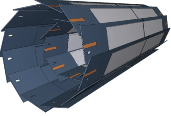
Having finished data taking in July 2010 the Belle detector will be upgraded to cope with the factor 40 increase of luminosity of the superKEKB machine presently being constructed at KEK in Japan. A major part of this upgrade is the replacement of the silicon vertex detector [1]. In the new detector the background and therefore the occupancy will be much higher. The outer layers will again use double sided silicon strip detectors. Due to the short sampling time of the APV ASICs ([2]) used for readout the very high background can still be tolerated. However, at the innermost radii the high granularity of a pixel detector is needed. Hence the inner two layers, at radii of 1.2 cm and 2.4 cm respectively, will be equipped with DEPFET pixel sensors (see Fig. 1). For Belle II a low material budget is one of the highest priorities. The low momentum tracks from B decays suffer from multiple scattering and an overall detector thickness of less than 0.2% X0 is required.
Hence the silicon sensors must be thinned and any additional material for support and cooling must be avoided.
Figure 1:Schematic view of the geometrical arrangement of the sensors for the PXD. The light grey surfaces are the sensitive DEPFET pixels, which are thinned to 75µm and cover the entire acceptance of the tracker system. The full length of the outer modules is 174 mm. The inner layer is at 1.2 cm radius, the outer at 2.4 cm respectively.
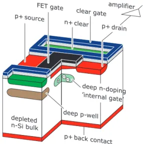
2.1 Operation principle of the DEPFET
The DEPFET was invented by Josef Kemmer and Gerhard Lutz in 1987 [3]. A p-channel MOSFET is integrated onto a silicon detector substrate which can be fully depleted (Fig. 2). A potential minimum for electrons is formed by sideward depletion [4] which is shifted directly un- derneath the transistor channel at a depth of about 1µm by an additional n-implantation underneath the gate. Incident particles or photons generate electron-hole pairs within the fully depleted bulk.
While the holes drift to the back contact, electrons are accumulated in the potential minimum, called the internal gate. If the transistor is switched on the electrons modulate the channel current.
The readout is non-destructive and can be repeated many times. To reset the detector signal charge and thermally generated electrons have to be removed from the internal gate. This process is called clear. A neighboringn+contact is pulsed at a positive voltage providing a punch-through into the internal gate. Thus the charge can be removed entirely avoiding any reset noise.
amplifier FET gate
p+ source
n+ clear
p+ drain clear gate
depleted n-Si bulk
p+ back contact deep n-doping
’internal gate’
deep p-well
Figure 2:Principle of a DEPFET.
The probably most important feature of the DEPFET is its very small capacitance of the inter- nal gate resulting in a very low noise performance, even at room temperature. Hence a sufficiently high signal to noise ratio (S/N) can be achieved with thin sensors. As the noise of the readout elec- tronics still dominates over the noise of the DEPFET theS/N of the system is proportional to the charge amplificationgq=∆Id/e−of the DEPFET. The relationship betweengqand the technology and design parameters is:
gq=gm/Cint (2.1)
wheregmis the transconductance of the external gate andCint is the capacitance of the internal gate. The gate length has the biggest impact ongq. Prototypes with the standard channel geometry have a gq of about 400 pA/e− but DEPFETs with a scaled channel geometry show even better results. For instance by decreasing the DEPFET gate length from L = 5µm to L = 4µm a gq of 560 pA/e−could be achieved.
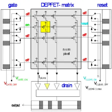
The individual pixels can be arranged in a matrix and readout in a rolling shutter mode. (Fig.
3): A matrix row is selected by pulling the external gate line to a negative potential using an external control chip. The selected DEPFET pixels send currents to the vertically connected drain lines. These currents are processed at the bottom of the matrix by the readout chip. The external gates just switch the pixel on and off while the signal amplification is achieved via the internal gate. There is no current flow in the non-selected DEPFET rows which leads to a very low power consumption of the array. A measurement cycle consists of a collection phase (Collect), the read out (Read) and the reset of the internal gate (Clear). A pedestal subtraction can be obtained either by a consecutive Read−Clear−Read sequence (double sampling) or by a faster Read−Clear procedure (single sampling) where pedestals are subtracted in the readout chip.
Figure 3:DEPFET matrix operated in rolling shutter mode.
2.2 Module concept
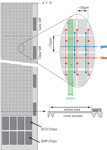
Figure 4 shows a sketch of the all-silicon-module for Belle II. The DEPFET pixel array is made on thin (≈75µm) detector grade silicon supported by a directly bonded silicon frame of≈400µm thickness. The read-out electronics, the lines for power, data, and slow control are located on the ends of the ladder outside the sensitive volume of the vertex detector. The switcher chips for the row-wise read out are attached on the thick frame along the long side of the ladder.
The pixel sizes for Belle II are 50 x 50µm2 and 50 x 75µm2 for the inner and outer layer of the Belle II vertex detector, respectively resulting in 256 x 1600 pixels per ladder. The most challenging requirement is the short frame readout time of 20µs which would leave for the given detector area and pixel size only 12.5 ns readout time per row which is by far too fast and would be incompatible with the intrinsic settling times on the long readout and control lines of the matrix.
To reduce the speed we decided to split the matrix, having readout electronics on both sides. In
z = 0
Gate SW
DCD Chips
clear
drains
~75µm gate
~50µm
active area cross section
Clear SW
DHP Chips
Figure 4: The all silicon module concept for Belle II with the readout and control ASICs bonded on the periphery of the DEPFET sensor module.
addition a high degree of parallelization is implemented. Four rows are read simultaneously which of course increases the number of drain lines and readout channels by the same factor. In total we gain a factor 8 which leads to a row processing time of 100 ns. Due to the already discussed rolling shutter mode the power consumed in the active sensor region can be kept in the range of about 0.1 W/cm2which still can be cooled by cold air.
As explained above the sensors need to be thinned to cope with requirement of a low material budget. For this purpose the DEPFET sensors will be produced on SOI material allowing a thick- ness of the active sensor region of only 75µm [5]. The processing sequence, explained in Fig. 5 allows for large monolithic all silicon sensor modules which, due to an integrated support frame, do not need any further support material. Furthermore, due to the low power consumption of the DEPFET pixel, no active cooling elements are needed in the sensitive region of the detector. Thus, even including frame and control ASICs (switcher) the overall material budget is only 0.19 % X0. 2.3 The readout and control ASICs and interconnections
Three different ASIC types are used for the matrix readout:
• The SWITCHER chip selects and clears the DEPFET four-row segments by generating volt-
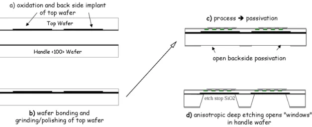
Figure 5: The process sequence for production of thin silicon sensors with electrically active back side implant starts with the oxidation of the top and handle wafer and the back side implantation for the sensor devices (a). After direct wafer bonding, the top wafer is thinned and polished to the desired thickness (b).
The processing of the devices on the top side of the wafer stack is done on conventional equipment; the openings in the back side passivation define the areas where the bulk of the handle wafer will be removed (c). The bulk of the handle wafer is removed by deep anisotropic wet etching and the etch process stops at the silicon oxide interface between the two wafers (d).
age swings of 10–20 V. In order to reduce the inactive module border, both functionalities are merged into a single chip. The channel selection is done internally by a simple shift register. Each chip can serve 32 matrix segments. Precise timing is provided by additional strobe input signals. The chip is produced in AMS 0.35µm HV CMOS technology.
• The DCD chip processes the currents of 256 columns and digitizes the analog values. Varia- tions of offset currents can be compensated by a two-bit DAC. The high sampling rate of 10 MHz is obtained by using two 8 bit ADCs per channel alternately. The chip is produced in UMC 180 nm technology.
• The DHP chip performs data processing, compression, buffering and fast serialization and sends the data off module to the data acquisition system. The chip is produced in IBM 90 nm technology.
The compact design of the modules requires a sophisticated interconnection technology to con- nect the ASICs to the DEPFET sensors. Due to the projective readout and control of the DEPFET matrix the overall number of channels to connect is rather low, not much different from a strip sensor of equal pitch, and simple wire bonding would still be an option. Indeed, this is used for prototyping. However, on the real module this would occupy too much space and add consider- able material. Hence flip-chip techniques and bump bonding will be used for the interconnection.
Fortunately the low number of interconnections allows for a rather large pitch (≈200 µm) and commercially available bump bonding can be used. The DCD and DHP ASICs will be equipped with the bumps by the vendor. Unfortunately this service is not offered for the switcher chip, made in AMS HV CMOS technology. Here we will deposit the solder bumps ourselves. The technology developed by ZITI, Heidelberg, consists of adding gold pads to the ASIC. The gold is deposited
to the Al pads of the ASIC with ultrasonic, similar to wire bonds, and flattened (’coined’). Then melted SnPb is spit on those pads by a commercially available machine (from PACTECH [6]) forming the solder balls.
The copper landing pads on the DEPFET sensors are grown using electroplating. Test per- formed with CNM, Barcelona, have shown that the copper deposition, including the necessary titanium-tungsten barrier layers does not harm the DEPFET properties. Presently the copper depo- sition is being installed as back-end process in our lab.
Once both ASICs and DEPFETs are processed the ASIC mounting can be done by rather coarse flip chip machines available in the institutes.
3. R&D towards a novel pixel detector for the sLHC
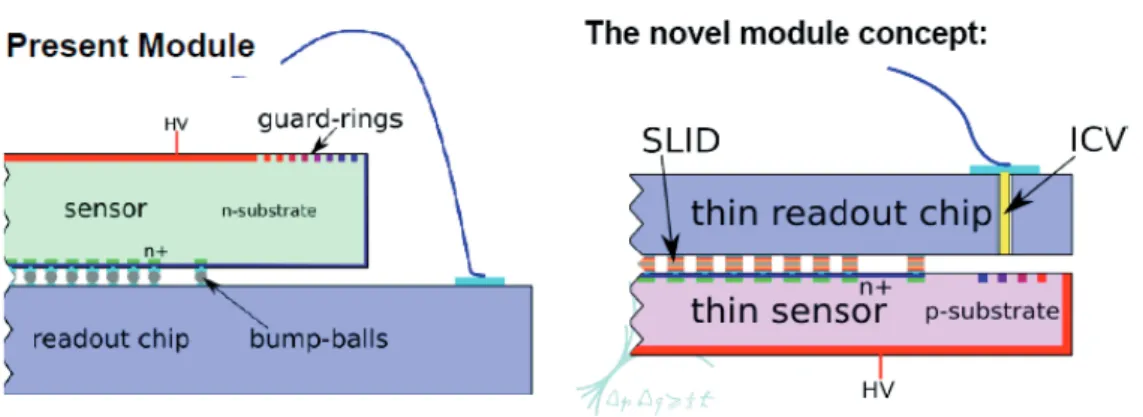
The present ATLAS pixel detector [7] is a hybrid pixel detector made from a pixel sensor with sixteen readout ASIC chips bump bonded to it. After ten years of operation at LHC this detector (and the complete ATLAS inner tracker) has to be replaced due to radiation damage. In addition an update of the LHC accelerator is planned, the super LHC (sLHC). The sLHC is expected to achieve an increase in luminosity of about a factor of ten. Consequently, for a given radius, the expected numbers for the radiation dose and hit occupancy at the sLHC are a factor 5–10 higher than at the LHC. Hence we started an R&D [8] effort to develop a new pixel detector concept overcoming the limitations of the present hybrid pixel concept (Fig. 6):
• The use of 75–150µm thin sensors will increase the radiation tolerance.
• A novel interconnection technology for attaching the readout electronics to the pixel sensors can lead to a cost effective solution to replace the presently used bump bonding technology.
It also has the potential to go to finer pitch increasing the detector resolution.
• Inter chip vias allow to contact the ASICs from the backside. Hence the cantilever design of the present module can be avoided leading to a simplified module design and to material reduction.
The idea is to build upon our experience of producing thin sensors [5], like developed for the DEPFET, which feature low depletion voltage, low leakage current and high charge collection ef- ficiency. At radiation doses of 1016neutrons/cm2(1 MeV equivalent) as foreseen at the sLHC the performance of silicon detectors will be limited by the trapping of the charge carriers reducing the effective thickness of a sensor to few tens of microns. Using our thinning technology described already in section 2.2 (Fig. 5) we developed thin detectors whose depletion voltages and leakage currents after irradiation will be low enough for stable operation. These detectors have been pro- duced using both p-in-n and n-in-n technology on SOI wafers with 75µm and 150µm thickness of the top wafers. First tests demonstrated the high charge collection efficiency of these detectors even irradiated to the highest fluences.
For the interconnection to the read out ASICs we use the Solid-Liquid InterDiffusion (SLID) technology [9] developed by the Fraunhofer Institute IZM [10] at Munich.
This process uses through-mask-electroplating of copper and tin layers on one contact side and copper only on the matching side to produce an eutectic bonding. The SnCu pillars are very
Figure 6:New module concept (right): Compared to the present ATLAS pixel module (left) the bump bonds are replaced by the IZM SLID interconnection. Inter chip vias (ICV) allow to contact the ASICs from the backside reducing considerable the dead cantilever region needed before to access the wire bond pads of the chip.
thin (5µm) and the pitch which can be achieved is only limited by the precision of the pick and place tools.
This high density interconnection technology could be used to achieve a smaller pixel size than in the current ATLAS hybrid pixel detector, which may be hard with the presently used bump bonding technique. Besides the interconnection of chips and sensors this technology allows for 3D integration of several thinned layers using the ICV-SLID process (Inter-Chip Vias together with the SLID process). The eutectic bonding forms an alloy with a melting point above the temperature needed to form the connection. Hence additional layers can be stacked without destroying the bonds already made. However, no rework is possible once the bonding is formed. Chips performing the analog and digital parts of the read-out can be arranged on top of each other rather than side by side. In addition, the chips can be made using different technologies and be optimised individually in terms of speed, power and radiation hardness, allowing for a better overall performance.
In our concept this feature is not yet used, we need the ICV only to create backside connectivity of the ASICs.
The first investigations to study the compatibility of the thin sensors produced at HLL with the various steps involved in the SLID process have been performed in collaboration with IZM. It has been found that the dark currents of small diodes do not deteriorate after applying the TiW, Cu and Sn layers, as well as heating to form the Cu3Sn alloy [11]. Since Cu diffusing into the silicon sensors would result in much increased leakage currents, this means that the TiW barrier layer is a proper protection of the silicon sensor.
The production of some simple test structures to investigate the precision of the positioning of chips onto the sensors, and the efficiency and reliability of the SLID contacts has been started and satisfactory results have been achieved. The inefficiency of SLID connection is at a level of 10−4. However, some problems have been experienced, like the need of carefully adjustment of the Sn thickness to the area of the SLID pad, to avoid shorts caused by surplus tin flowing out of the pad.
The chip-to-wafer assembly used makes it necessary to place the individual ASICs on a handle wafer which is then bonded on the sensor wafer. Good yield is only achieved if the population density of the handle is uniform and all chips have equal thickness.
Although the assembly is in principle chip-to-wafer, it is necessary to have the ASIC chips still on a wafer in order to perform various preprocessing steps (copper plating, thinning) before the chips are diced and assembled on the handle wafer.
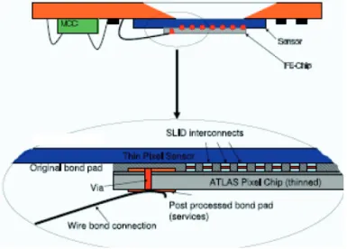
The next step, presently in work, is the construction of a demonstrator module using the thinned silicon sensors and ATLAS FEI-3 readout chips [12] which are still available on wafers hence the preprocessing steps mentioned above can be performed. This demonstrator (Fig. 7) has all the essential features of the new module concept. In addition it will show if it is possible to add vias to a standard ASIC chip, not designed for 3D integration, by postprocessing. This is not trivial since the via etching requires areas in the chip which are free from active elements and dummy filling structures. Fortunately in the case of the FEI-3 such areas close to the service pads could be identified. To date the preprocessing of the sensor and ASIC wafers is progressing, including via etching. The interconnection will be done in the near future.
Figure 7: Demonstrator for the 3D module concept: An ATLAS FEI-3 chip postprocessed with vias for SLID interconnection is bonded on a matching thin pixel sensor. The vias allow to contact the service pads of the FEI-3 chip from the backside. The assembly is mounted on a PCB with the necessary auxiliary components (MCC - module control chip).
4. Summary
For the vertex detector of Belle II a small, but precise pixel detector is needed. The low mo- mentum tracks in this experiments require a low mass detector, which still has to have high readout speed and sufficient radiation hardness. A DEPFET active pixel sensor fulfill these requirements.
The all silicon detector module features thin sensor material a self supporting module structure and only few small ASICs in the active area. Due to the low power consumption the active area can be kept free from any cooling infrastructure. The compactness of the modules requires bump bonding of the ASICs to the DEPFET sensor. However, due to the rather low interconnection density stan- dard bump bonding technologies, supported by industry, can be used and the actual flipping can be made in house.
The requirements for a ATLAS pixel detector for the sLHC upgrade are completely different.
Though material is an issue other items, like radiation hardness and low cost, fine pitch intercon- nections are more important. The proposed concept is an evolution of the hybrid pixel detector as already used in ATLAS. However, the bump bonding will be replaced by a 3D integration tech- nology and interchip vias allow to contact the ASICs from the backside. Radiation hardness is addressed using thin sensors. A demonstrator module should show the feasibility of this concept, especially the possibility to prepare existing conventional CMOS ASICs for 3D integration by postprocessing.
References
[1] T. Bergauer,The Silicon Vertex Detector of the Belle II Experiment, these proceedings.
[2] M.J. French, Nucl. Instr. and Meth. A466, 359, (2001).
[3] J. Kemmer, G. Lutz,New semiconductor detector concepts, Nucl. Instr. and Meth. A253, 356, (1987).
[4] E. Gatti and P. Rehak, Nucl. Instr. and Meth. A225, 608 (1984).
[5] L. Andriceket al.,Processing of ultra-thin silicon sensors for future linear collider experiments, IEEE Transactions on Nuclear Science 51, 1117-1120 (2004).
[6] P. Kasulke, W. Schmidt, L. Titerle, H. Bohnaker, T. Oppert, E. Zakel,Solder Ball Bumper SB2-A flexible Manufacturing Tool for 3-dimensional Sensor and Microsystem Packages, Proceedings of the 22nd International Electronics Manufacturing Technology Symposium (Berlin, Germany), Apr. 27-29 (1998).
[7] The ATLAS Collaboration and G. Aad et al. JINST 3 S08003 (2008) doi:
10.1088/1748-0221/3/08/S08003.
[8] R. Nisiuset al.,R&D on a novel interconnection technology for 3D integration of sensors and electronics and on thin pixel sensors, ATL-P-MN-0019, ATLAS internal document, (2007).
[9] A. Klumppet al.,Vertical System Integration by Using Inter-Chip Vias and Solid-Liquid InterDiffusion Bonding, Japanese Journal of Applied Physics 43, No 7A.
[10] Fraunhofer-Institut für Zuverlässigkeit und Mikrointegration IZM, Institutsteil München, Hansastraße 27d, 80686 München, Germany.
[11] A. Macchioloet al.,Development of thin pixel sensors and a novel interconnection technology for the SLHC, 9thInternational Workshop on Radiation Imaging Detectors, Erlangen, Germany, 22-26 July 2007, Nucl. Instr. and Meth. A591, 229-232 (2008)
[12] I. Peric et al., Nucl. Instr. and Meth. A565, 178 (2006).