D is se rt at io ns re ih e P hy si k - B an d 4 0 Johannes Kar ch
Raman spectroscopy of nanopatterned graphene Stefanie Heydrich
40
9 783868 451108
ISBN 978-3-86845-110-8
Stefanie Heydrich
ISBN 978-3-86845-110-8
cations nanopatterning is necessary. For graphene spintronics, pure zigzag edges are additionally required. It is therefore necessary to study the influence of nanopatterning and to verify attemps at cre- ating pure zigzag edges.
To adress the first issue, the work at hand comprises a Raman study of a series of samples of singlelayer graphene patterned with square antidot lattices. We have found this nanopatterned graphene to be p-type doped with the doping concentration tentatively depending on the number of antidots per square unit.
An attempt at creating pure zigzag edges has been made via an anisotropic etching process applied to square antidot lattices on sin- glelayer graphene. This thesis shows a step-b-step Raman evaluation of the etching process and verifies via inter-valley scattering that it indeed results in predominantly zigzag edges.
Stefanie Heydrich
Raman spectroscopy of nanopatterned graphene
Herausgegeben vom Präsidium des Alumnivereins der Physikalischen Fakultät:
Klaus Richter, Andreas Schäfer, Werner Wegscheider
Dissertationsreihe der Fakultät für Physik der Universität Regensburg, Band 40
der naturwissenschaftlichen Fakultät II - Physik der Universität Regensburg vorgelegt von
Stefanie Heydrich aus Nürnberg im Februar 2014
Die Arbeit wurde von Prof. Dr. Chrstian Schüller angeleitet.
Das Promotionsgesuch wurde am 12.02.2014 eingereicht.
Das Kolloquium fand am 03.06.2014 statt.
Prüfungsausschuss: Vorsitzender: Prof. Dr. V. Braun 1. Gutachter: Prof. Dr. C. Schüller 2. Gutachter: Prof. Dr. D. Weiss weiterer Prüfer: Prof. Dr. S. Ganichev
Stefanie Heydrich
Raman spectroscopy of
nanopatterned graphene
sind im Internet über http://dnb.ddb.de abrufbar.
1. Auflage 2014
© 2014 Universitätsverlag, Regensburg Leibnizstraße 13, 93055 Regensburg Konzeption: Thomas Geiger
Umschlagentwurf: Franz Stadler, Designcooperative Nittenau eG Layout: Stefanie Heydrich
Druck: Docupoint, Magdeburg ISBN: 978-3-86845-110-8
Alle Rechte vorbehalten. Ohne ausdrückliche Genehmigung des Verlags ist es nicht gestattet, dieses Buch oder Teile daraus auf fototechnischem oder elektronischem Weg zu vervielfältigen.
Weitere Informationen zum Verlagsprogramm erhalten Sie unter:
www.univerlag-regensburg.de
Contents
Contents i
1 Précis 1
2 Motivation and Overview 3
2.1 Graphene . . . 3
2.2 Raman spectroscopy . . . 5
2.3 Nanopatterning graphene: Antidots and zigzag edges . . . 6
3 Fundamental properties of graphene and Raman scattering in graphene 9 3.1 Fundamentals of Raman scattering . . . 9
3.2 Graphene - crystal lattice, band structure and phonon dispersion . 11 3.2.1 Crystal lattice of graphene and stacking order of multilayer graphene . . . 11
3.2.2 Electronic bands and phonon dispersion . . . 13
3.3 Raman scattering in graphene . . . 16
3.3.1 Raman modes in graphene . . . 16
3.3.2 Inuence of the number of layers on the 2D mode . . . 21
3.3.3 Inuence of edge chirality on the D mode . . . 22
3.3.4 Inuence of charge carriers on the G and 2D modes . . . . 24
4 Sample fabrication and experimental setup 27 4.1 Sample fabrication and samples . . . 27
4.1.1 General preparation of single layer graphene and substrate 27 4.1.2 Single layer graphene with backgate . . . 28
4.1.3 Single layer graphene with circular antidots . . . 28
4.1.4 Single layer graphene with hexagonal antidots . . . 31
4.2 Experimental setup . . . 33
5 Experimental results 35
i
5.1 Basic information to scanning Raman spectroscopy in graphene . 35 5.2 G peak position and lineshape in single layer graphene with backgate 39 5.3 P-type doping in single layer graphene with circular antidots . . . 43 5.4 Raman study of anisotropically etched hexagonal antidots in single
layer graphene . . . 49
6 Conclusion and outlook 59
6.1 Conclusion . . . 59 6.2 Outlook . . . 60
Bibliography 61
Chapter 1
Précis
Graphene is valued for its high charge-carrier mobility, its exibility and trans- parency, its ability to withstand mechanical stress, and, not least, the fact that it is a two-dimensional material, whose existence was predicted to be forbidden by theory [Pei35] [Lan37]. Due to theses properties, graphene readily lends itself to many applications in electronics, opto-electronics, sensing, the construction of het- erostructures with other two-dimensional materials, and many other elds. One hope for the future is that graphene may succeed silicon as base material for elec- tronics, as silicon-based electronics will very soon reach their performance limit and graphene is among the best alternatives. However, graphene has no intrinsic band gap, which severely hurts the construction of graphene eld-eect transistors and generally the transfer of Si-based electronics to graphene-based electronics.
Several ways have been found to successfully address this issue, among them the periodic patterning of graphene with antidots, which opens a band gap. However, the eect of nanopatterning on graphene has not been studied in depth.
Theorists have predicted a spin-polarized edge state in graphene along perfect zigzag edges, making graphene a material perfect for spintronic applications.
However, graphene akes with perfect zigzag edges have not yet been realized, removing the possibility of graphene spintronics even further into the future than the hope for graphene electronics.
This work will concentrate on the eect of nanopatterning realized through pe- riodic antidot lattices in graphene and the preparation of predominantly zigzag edges. We have prepared a series of samples of single layer graphene akes with square antidot lattices with dierent lattice constants ranging from 80 nm to 400 nm and two sizes of antidot diameters (50 nm and 60 nm). Scanning Raman spectroscopy on patterned samples showed an increase of the D peak intensity and a decrease of the G peak intensity as well as stiening, that is an up-shift of the G mode position. The former two are due to articial introduction of defects
1
and decrease of graphene per unit area by the antidots, respectively, while we attribute the latter to doping. Through careful evaluation of the positions of G and 2D modes, we have determined the graphene antidot lattices to be p-type doped with charge carrier concentrations ranging from 3×1012 cm−2 in the 400- nm sample to 7×1012 cm−2 in the 80-nm sample.
Additionally, we have studied the preparation process of a large single layer graphene ake patterned with two types of square antidot lattices with 200 nm and 400 nm lattice constant, respectively, that have predominantly zigzag edges resulting from anisotropic etching. This ake is in contrast to graphene akes with usual antidots, whose edges contain both zigzag and armchair edge congu- rations in comparable amounts. The ake was processed in ve steps - exfoliation from natural graphite (1), patterning of conventional antidots via electron beam lithography and reactive ion etching (2), a preparation step (3), and two successive anisotropic etching steps (5). Only one anisotropic etching step is necessary; we added another to see, if prolonged etching increases the ratio of zigzag to armchair edges. After each step, we performed two Raman scans, one monitoring the D and G peak and one monitoring the 2D peak. Since the D peak probes intervalley scattering, which is forbidden for pure zigzag edges, we evaluated the D peak in- tensity for each step and have found the antidot edges to be predominantly zigzag after the anisotropic etching. Two anisotropic etching steps were performed to see if continued etching would increase the zigzag-to-armchair ratio and we have found this to be the case.
We have also determined doping after each preparation step in the area where the 200 nm antidot lattice was etched and have found the ake to be p-type doped af- ter every step like the conventional, circular antidots, ranging from 4.5×1012cm−2 after the preconditioning step to 9×1012 cm−2 after the nal anisotropic etching step.
Chapter 2
Motivation and Overview
This chapter is designed to give an overview of the eld this work is associated with. We will rst discuss prior research on graphene, its properties, and appli- cations, insofar as they have been realised, and areas where information is still scarce. We will then introduce the merit of Raman spectroscopy as an inves- tigative tool, highlighting its role in graphene research. Thirdly, the concept of antidots will be introduced. We will summarize their eects on graphene, as they have been discussed in literature. Lastly, we will name some advantages gained by being able to fabricate graphene devices with dened edge-chiralities. We will nish by embedding the research presented in this work into the context of state- of-the-art graphene research.
2.1 Graphene
This section introduces the material graphene in general terms, touching on its many desirable qualities and noting several areas where graphene is a promising candidate, like optoelectronics, electronics, and heterostructures, and the progress in research and development achieved there.
Graphene is a two-dimensional carbon allotrope and, after sixty years of theo- retical study [Wal47] [Tia94] [Nak96] [Woo00] [Gon01] [Rei02], the rst quasi- freestanding two-dimensional solid to have been isolated [Nov04]. Fundamental research favors graphene obtained by the so-called mechanical cleaving method rst described in 2004 [Nov04], which has since been rened [Nov05], because it produces mostly clean, unstrained graphene. However, akes are small, ranging from a few to a few 100 µm in size, randomly deposited on a substrate. For many applications, production methods like chemical vapor deposition (CVD) [Li09]
3
and epitaxial growth on SiC [Ber06] [Oht06] are preferable, since they yield large akes, in the range of several tens of inches [Bae12]. Graphene has also been synthesized using liquid-phase exfoliation [Her08].
The development of dierent isolation methods allowed, after years of theoretical exploration only, experimental research into graphene's many exciting properties.
It is two-dimensional, it is extremely sti, yet strong and elastic, it conducts both heat and electric current exceptionally well, it is transparent. These qualities make graphene an ideal candidate for a number of applications and, understand- ably, research is intense.
In electronics, for example, graphene is valued for its conductive capabilities and exibility. It can be used to realize exible electrodes in organic light emitting diodes (OLEDs) [Han12] and solar cells [Wan08]. Since it is also transparent, it has been used as transparent electrode in a touch-screen [Bae12]. Its high carrier- mobility is invaluable in high-frequency transistors [Lia10] [Wu10] [Lin11], exceed- ing state-of-the-art silicon transistors of the same gate length [Lin10a]. However, pristine graphene has no band gap, which prohibits switching o in eld eect transistors, so many attempts have been made to open a - preferably continu- ously scalable - band gap while maintaining the excellent transport properties.
One scheme is through quantum connement in graphene nanoribbons (GNR) [Son06a] [Han07], however, the size of the gap is very sensitive to ribbon width and the atomic conguration of the edge, and narrow ribbons are incapable of carrying large currents. Other attempts are substrate- [Hic13] [Zho07] or strain- induced [Ni08b] [Gui10] bandgaps; the rst is not tunable and the tunability of the latter is limited by the amount of strain the graphene can take without breaking.
The most promising candidate to open a bandgap in graphene is nanopatterning, by hydrogen passivation [Bal10], boron or nitrogen doping [Ci10], and antidots [Ero09]. The latter will be discussed in more detail below.
Graphene is also a promising candidate for opto-electronics. It can be turned into a photodetector [Xia09] or a solar cell [Mia12]. It can be used as a saturable absorber in mode-locked lasers [Sun10] with ultrawideband tunability [Zha10] or in passively Q-switched lasers [Pop11].
Another possible application for graphene is in the elds of sensors [Koc12] and bio-sensors [Kui11].
Preparation of graphene has also spawned research into other two-dimensional ma- terials like boron nitride (BN) [Nov05], NbSe2 [Nov05] [Col11], TaSe2 [Col11] and molybdenite (MoS2) [Nov05] [Mak10] [Kor11] [Rad11] [Ple12b] [Ple12a]. Combi- nations of these materials lead to heterostructures, which can e.g. be made into high-frequency transistors [Bri12].
Graphene may also be used as a substrate. In transmission electron microscopy (TEM) [Nai10], molecules are placed on a graphene single layer, which is draped over a hole in the sample holder. In Raman spectroscopy, molecules on graphene exhibit an enhanced signal compared to the conventional substrate SiO2 [Lin10b]
and a frequency shift [Yag12]. This is called graphene-enhanced Raman scattering
2.2. RAMAN SPECTROSCOPY 5
(GERS).
2.2 Raman spectroscopy
This section concentrates on the merits of Raman spectroscopy as an investigative tool in general and its advantages when used to analyze graphene in particular.
Raman scattering is an inelastic scattering process of a photon creating or anni- hilating an excitation in the probed material. Comparing the energy of incoming and scattered photon yields information about allowed excitations in the material.
In 1928, C. V. Raman and K. S. Krishnan observed the Raman eect in liquids [Ram28], and G. Landsberg and L. I. Mandelstam in crystals [Lan28]. It had been predicted theoretically in 1923 by A. Smekal [Sme23] to probe vibrational, rota- tional and other, low-frequency modes in a system, giving information about the intrinsic make-up of the sample. The fact that it is very fast and non-destructive and can, when combined with a microscope, be used to probe samples with sub- µm resolution makes it a very attractive method.
Therefore, Raman spectroscopy is frequently used to analyze both liquid samples and crystals. In chemistry and biology, liquid samples are probed most commonly to gain specic knowledge about chemical bonds and symmetries in molecules, re- sulting in a Raman ngerprint for each specic molecule. In solid-state physics, crystals are probed to learn about their phonon dispersion, to measure tempera- ture and to determine the crystallographic orientation.
In graphene, Raman spectroscopy has been used to probe the phonon dispersion [Rei04]. It can determine the number of layers in few-layer samples [Fer06] by sounding the electronic structure in the sample, which evolves with the number of layers. The Raman spectrum in single layer graphene changes with doping [Yan07] [Pis07] [Das08], making it possible to determine charge carrier densities via Raman spectroscopy [Hey10]. Uniaxial [Ni08b] and biaxial [Met10] strain in graphene single layers leave ngerprints in the Raman spectrum. Already in 1970, the eects of grain boundaries in nanocrystallite graphite on the Raman spectrum have been studied [Tui70]. After the discovery of graphene, this research was ex- tended to graphene, researching both dierent kinds of defects and concentrations of defects using Raman scattering [Cas07] [Cas09a] [Can11] [Eck12]. Scanning Ra- man spectroscopy can not only give single spectra at one position on a sample, but image the topology of a ake. This can be used to determine the edge chirality and, ultimately, the crystal orientation [You08] [Cas09b] of a given ake.
2.3 Nanopatterning graphene: Antidots and zigzag edges
The rs part of this section introduces the concept of antidots and covers their part in graphene research. The second part concentrates on the possibility of graphene devices with perfect zigzagedges being used to realize spintronics and the experimental progress made in this direction.
An antidot lattice is an array of holes etched into the sample, designed to super- impose a periodic potential landscape on the sample. Antidots can be arrayed in rows and columns with equal distances and are then called a square lattice, or in a hexagonal, or a triangular fashion. Antidots were rst introduced in GaAs-AlGaAs heterojunctions as a square array of microscopic holes etched into a high-mobility 2DEG conductor, where anomalous low-eld Hall plateaus and a quenching of the Hall eect about B=0 were observed [Wei91]. Weiss et al. calcu- lated that the antidots interrupt classical commensurate orbits of charge carriers, causing the observed eects. Later, quantum oscillations in magnetotransport in similar samples were reported [Wei94].
Graphene patterned with an antidot lattice exhibits prominent absorption res- onances in the microwave and terahertz regions due to surface plasmons in the graphene disturbed by the superlattice [Nik12]. Recently, coupling of such plas- mons in graphene antidot lattices to substrate phonons has been observed exper- imentally and described theoretically [Zhu13].
As already mentioned above in the section on graphene, imposing a superstruc- ture via antidot lattices leads to the opening of a bandgap in graphene in the range of several meV [Ero09] [Pet11]. Dierent lattice types, square, hexagonal, or triangular, create larger or smaller band gaps [Ouy11]. The position of the individual antidots with respect to the underlying graphene lattice also inuences the size of the gap [Dvo13].
Etching antidot lattices into graphene also introduces p-type doping in the ake [Hey10] [Beg11]. In both cases, Raman spectroscopy was employed to quantify the amount of doping.
Manipulating a graphene antidot lattice by leaving out some of the antidots cre- ates defect states or pairs of coupled defect states in the antidot lattice, which can function as hosts for electron spin qubits [Ped08].
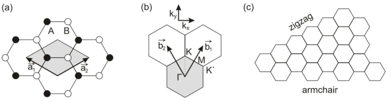
Owing to its honeycomb-like atomic structure, graphene can have two types of ordered edges: so-called armchair and so-called zigzag edges. (See chapter 3 for more information on edge chirality.) Along a pure zigzag edge, an exception- ally large local electron density and a spin polarized edge state were predicted [Son06b] [Wim08] [Yaz08], making graphene the perfect material for spintronic applications. So far, edge states have been detected using e.g. STM to investi- gate graphene nanoribbons [Zha13], but spin polarized edge states have only been proposed in theory. Production of perfect zigzag edges is still a great challenge
2.3. NANOPATTERNING GRAPHENE: ANTIDOTS AND ZIGZAG EDGES 7
and so far, no devices have been realized. It has been possible, however, to etch antidots with dominating zigzag edges [Kra10] [Obe13]. In both cases, Raman spectroscopy was used to determine the edge chirality. In the latter, weak local- ization was additionally employed.
Chapter 3
Fundamental properties of
graphene and Raman scattering in graphene
In this chapter, both graphene and Raman scattering will be introduced. The chapter begins with a short, basic introduction into Raman scattering in general, highlighting resonant and double-resonant Raman processes. In the second part, we will discuss single-, bi-, and multilayer graphene and graphite in terms of its atomic conguration and the resulting electron and phonon dispersions. The most prominent Raman modes in graphene will be briey introduced. In the last part of this chapter, all Raman modes in graphene examined in the experimental part of this work, namely the G, D, D0 and 2D peaks, will be discussed in depth. This discussion will include the inuence of the number of layers in a sample, charge carriers, and edge chirality on certain peaks.
3.1 Fundamentals of Raman scattering
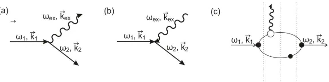
Raman scattering (sometimes also called combination scattering) is an in- elastic scattering process of light on a medium, creating or annihilating an excita- tion in the material. The scattering process is then called Stokes or Anti-Stokes process, respectively, as depicted in Fig. 3.1(a) and (b). In both cases, energy conservation
~ω1 =~ω2±~ωex (3.1)
9
Figure 3.1: Feynman diagram for a (a) Stokes and (b) Anti-Stokes scattering pro- cess. The solid straight lines indicate photons, the wavy line depicts the excitation in the material. (c) Feynman diagram for a second-order Raman process. The incoming light creates an electron-hole pair, the electron is scattered by a phonon (white circle), the hole is then scattered by a defect (black circle) before electron and hole recombine. The vertical dashed lines indicate intermediate states.
where ω1 denotes the frequency of the incoming photon, ω2 the frequency of the scattered photon and ~ωex the energy of the created or annihilated excitation, and momentum conservation
~~k1 =~~k2±~~q+~K~ (3.2) with~k1 denoting thek-vector of the incoming photon,~k2 thek-vector of the scat- tered photon, ~q the k-vector of the excitation and K~ a vector of the reciprocal lattice, must be fullled. For the purposes of this work, the incoming photon creates an electron-hole pair and the excitation is always a phonon.
Since typical experiments are conducted using light sources in the 1064 - 229 nm range and the lattice parameter a is of the order of a few Å, (≈ 2,46 Å in graphene), k1, k2 π/a(see e.g. supplementary information of [Fer13]). Then follows from eq. 3.2, that the phonon wave vector q ≈ 0 in rst-order scatter- ing. This is dubbed the fundamental Raman selection rule. In rst or- der, only scattering processes involving a phonon near Γ are Raman-allowed.
Scattering processes involving only one phonon with large k-vector are Raman- forbidden and require a defect for momentum conservation. One example is shown in Fig.3.1(c). Therefore, such scattering processes can only take place at defect sites, never in the perfect crystal. The emission (or absorption) of two phonons, however, can always satisfy eq. 3.2: q+ (−q) = 0.
The intensity of a Raman peak is contingent on the dierential scattering cross section dσ for the Raman scattering of an initial photon (~k1, ω1) into the solid angle dΩ which in turn depends on the matrix elements K2f,10 as (see e.g. (3.6) of [Mar83])
dσ(~k1ω1) =|K2f,10|2(~ω1−Ef)2dΩ/(4π2~4c4) (3.3) when Ef denotes the nal energy of the system.
Since Raman scattering is a scattering process of light on a medium, its cross
3.2. GRAPHENE - CRYSTAL LATTICE, BAND STRUCTURE AND PHONON
DISPERSION 11
section depends on the interaction between radiation and matter, described by the radiation-matter-interaction Hamiltonian HRM. K2f,10 describes the matrix elements which contribute to the scattering cross-section. The indices 0, f ofK2f,10 refer to the ground and nal phononic state, respectively, the indices 1, 2 denote the incoming and outgoing photon.
For a rst order process, the matrix elements K2f,10 can be expressed in second order perturbation theory as ((3.31) in [Mar83])
K2f,10=X
i,j
Mf jMjiMi0
~2(ω1−ωi−iγi)(ω1−ωj−iγi) (3.4) whenMf j ≡< f|HRM|j >andMi0 ≡< i|HRM|0>denote the constant matrix el- ements of the radiation-matter-interaction, Mji ≡< j|Hep|i >denotes the matrix element of the electron-phonon-interaction with Hep the Hamiltonian describing the electron-phonon interaction, and γi is the broadening parameter.
For an n-phonon process, eq. 3.4 can be expanded to [Mar83]
K2f,10= X
s0,...,sn
Mf s0Ms0s1...Msn−1snMsn0
~n+1(ω1−ωs0 −iγs0)(ω1−ωs1 −iγs1)...(ω1−ωsn−1 −iγsn−1)(ω1−ωsn −iγsn). (3.5)
Typically, all intermediate energy states involved in a Raman scattering process are virtual. Since the scattering process happens on a very short timescale, the uncertainty principle
∆E∆t ≥ ~
2 (3.6)
where∆E is the energy dierence from the virtual state to the next eigenstate and
∆t is the lifetime of the virtual state, allows the violation of energy conservation for intermediate states. This does not aect energy conservation of the overall process.
However, if one intermediate state is an eigenstate of the material, the scattering process is called resonant and eq. 3.5 diverges. If, in a higher order process, two (three) intermediate states are real, this is called a double (triple) resonance.
3.2 Graphene - crystal lattice, band structure and phonon dispersion
3.2.1 Crystal lattice of graphene and stacking order of mul- tilayer graphene
single layer Graphene is a two-dimensional material made of sp2-hybridized carbon atoms. Each carbon atom is covalently bound to its three neighboring
Figure 3.2: (a)real space representation of graphene. The lattice is spanned by two basis vectors~a1,~a2 framing the rhombic unit cell, shaded light gray. Black and white circles denote carbon atoms of the two sublattices. (b)reciprocal space. The shaded hexagon represents the rst Brillouin-zone,~b1 and~b2 denote the primitive vectors and K, K0 and M mark points of high symmetry. kx and ky identify the coordinate axes in reciprocal space. (c)real space representation of the graphene lattice exhibiting a zigzag and an armchair edge.
atoms. The crystal structure consists of a rhombic unit cell, with two inequiva- lent base atoms A and B, spanned by base vectors~a1 and~a2 with lattice constant
|~a1|=|~a2|= 2.461 Å . The distance between neighboring carbon atoms isaC−C = 1.42 Å. This array results in the well-known honeycomb lattice with two sublat- tices A and B as may be seen in Fig. 3.2(a). In reciprocal space, the rst Brillouin zone is a honeycomb with corners denotedK andK0, since they are not connected by primitive vectors of the reciprocal lattice~b1 and~b2 and thus inequivalent, see Fig. 3.2(b). The edge of a graphene ake is typically made up of a combination of two atomic congurations called zigzag and armchair, shown in Fig. 3.2(c).
single layer graphene consists of only one carbon layer, in bilayer graphene, two single layers are stacked on top of each other, following the A-B Bernal stacking with an interlayer distance of 3.35 Å. Bernal stacking means that the top layer is shifted rigidly in-plane by aC−C with respect to the bottom layer so that all atoms of sublattice A in the top layer lie over atoms of sublattice B in the bottom layer. All atoms in sublattice B of the top layer have no carbon atoms directly underneath in the bottom layer. Bilayer graphene exfoliated from graphite will follow this stacking order.
It is also possible to nd two layers of graphene not following the Bernal stacking.
Epitaxially grown graphene may consist of two or more rotated layers, exhibiting a ngerprint Moiré pattern in STM images [Pon05]. This is called twisted graphene and its electronic properties dier from those of bilayer graphene [Li10a]. Another kind of two-layer graphene is folded graphene. It is created articially from single layer graphene akes on SiO2 by ushing acetone or other liquids over the sample, folding part of a ake back in on itself or by growing graphene through chemical vapor deposition (CVD) on specially prepared copper foils. The latter method
3.2. GRAPHENE - CRYSTAL LATTICE, BAND STRUCTURE AND PHONON
DISPERSION 13
Figure 3.3: (a) two-dimensional band structure of graphene depicting both the π and theσbands. Theπ andπ∗ bands cross at the Fermi level, forming valence and conduction band. Image from [Li10b] (b) three-dimensional image of the graphene valence and conduction band, obtained through tight-binding calculations. The π and π∗ bands are linear around K and almost mirror each other. Image from [Kat07].
allows position control of the fold [Kim11]. In both cases, the folding inuences the electronic properties of the graphene, e.g. reducing the Fermi velocity [Ni08a].
Multilayer graphene consists of three or a few more layers and can be stacked following either an A-B-A-B or an A-B-C stacking sequence where the third layer is shifted rigidly in-plane with respect to the second layer byaC−C like the second layer is to the rst. Both stacking orders may be found in natural graphite, but A-B-A-B Bernal stacking is much more common than A-B-C stacking. In this work, we will limit ourselves to A-B-A-B Bernal stacked samples.
3.2.2 Electronic bands and phonon dispersion
Graphene is often called a semi-metal or a gapless semiconductor. The reason for this is evident from graphene's bandstructure, shown in Fig. 3.3. As men- tioned above, graphene consists of sp2-hybridized carbon atoms, each of which is covalently bound to three neighboring atoms. The pz orbitals form the π valence and π∗ conduction band, which cross at the Fermi level at the K and K0 points, also called Dirac points in the context of electronic bands. The Fermi surface of graphene therefore consists of 6 points, only two of which are geometrically in- equivalent. In the vicinity of the Dirac point, both valence and conduction band are linear and almost mirror each other, inducing many of graphene's character- istic qualities. Fig. 3.3(a) shows a two-dimensional representation of both the π and the σ bands, formed by the in-plane bonds of graphene. The energy gap
Figure 3.4: (a) phonon dispersion of graphite (adapted from [Mau04b]). Solid lines are ab initio calculations, lled circles are experimental data gathered by in- elastic x-ray scattering, the dashed red line is a cubic spline connecting the experi- mental data for the TO branch. The light blue squares mark the phonon branches contributing most to the indicated peak. Inset: Brillouin zone of graphene with high-symmetry pointsΓ, K, and M. (b) table of most prominent Raman features in graphene and graphite. Listed are the name most common in literature, order of the Raman process, whether the scattering process is Raman allowed, the involved phonon branch(es), and the position of the mode in the spectrum.
3.2. GRAPHENE - CRYSTAL LATTICE, BAND STRUCTURE AND PHONON
DISPERSION 15
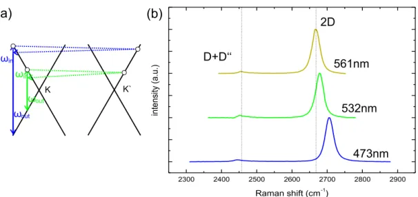
Figure 3.5: (a) schematic of two double-resonant scattering processes with dif- ferent excitation energies. The resonance condition necessitates dierent phonon k-vectors for dierent laser energies. (b) D+D00 peak and 2D peak in graphene measured with 473 nm, 532 nm, and 561 nm excitation wavelength. Both shift position if the excitation wavelength is changed.
between the σ bands is very large and they are far away in energy (of the order of tens of eV) from the Fermi point. Therefore, the valence- and conduction bands are formed by the π and π∗ bands around K. A three-dimensional diagram of graphene's π bands is shown in Fig. 3.3(b), where their similarity and linearity around the K points is particularly striking. For a theoretical discussion of the electron dispersion, see e.g. [Wal47],[Slo58] and [Par06].
Fig. 3.4(a) shows the phonon dispersion of graphite, obtained by ab initio cal- culations (solid lines) and corroborated by experimental data garnered by x-ray scattering (colored dots)[Mau04b]. The in-plane optical phonons are degenerate at the Brillouin-zone center and softened by a Kohn anomaly, as is the transversal- optical (TO) phonon at the K point [Pis04]. A Kohn anomaly is a softening of phonons in metals caused by electrons screening the lattice vibrations and coupled to kF. Therefore, the shape of the Fermi surface determines, where such a kink in the phonon dispersion appears. The Fermi surface of graphene consists of six points connected by the vector K~ and a Kohn anomaly may consequently only be found at Γ and K [Koh59][Pis04]. For a more detailed discussion of the phonon dispersion, see e.g. [Sai02], [Mau04a] and [Mau04b].
Fig. 3.4 (b) shows an overview of the most prominent Raman modes in graphene.
The table lists the name by which the peak is most often referred to in literature, the order of the Raman scattering process and whether it is Raman allowed or requires a defect to be activated, the corresponding phonon branch and the posi- tion of the peak in the Raman spectrum in cm−1. The 2D0 peak (in literature also
dubbed 2G peak and - mistakenly - assigned as second overtone of the G peak) is the second overtone of the D0 peak and stems from two LO phonons near Γ (see also blue square in Fig. 3.4(a)). Since the two phonons have opposite momenta, it is Raman allowed and may be observed anywhere on a graphene or graphite ake. It is caused by a double-resonant process and positioned around 3240 cm−1 if an excitation wavelength of 532 nm or approximately 2,33 eV is used. The 2D0 peak, like all peaks in graphene caused by a double-resonant process, is disper- sive, that is, its position is dependent on the excitation wavelength. The reason for this is sketched in Fig. 3.5(a): Dierent excitation wavelengths link valence- and conduction band resonantly for dierent wavevectors, requiring a dierent phonon k-vector for the double-resonant process. Since in each case, the phonon branch is probed at a dierent value ink-space, the phonon energy and thus the peak position may be dierent. Fig. 3.5(b) shows this in the cases of the D+D00 peak, which shifts rather slowly with excitation energy, and the 2D peak, which is strongly dispersive.
The D+D00 peak is found at about 2450 cm−1. It stems from a double-resonant scattering process involving a TO and an LO phonon from around the K point and its position is also sensitive to the excitation wavelength. It is Raman-allowed and therefore visible in defect-free graphene. For more details regarding this mode, see [Maf07]. The C mode is a rigid-layer shear mode only found in graphene with two or more layers. It can be used to determine the number of layers in a sample but due to its position close to the Rayleigh-scattered light in the spectrum it is quite challenging to measure [Tan12]. The N mode is another mode employed to determine the number of layers in a sample. It stems from a Stokes-Anti-Stokes combination of an LO phonon and a rigid-layer compression mode of graphite [Her12]. The G, D, 2D and D0 peaks will be discussed in detail below.
3.3 Raman scattering in graphene
This section concentrates on the concrete example of phonon generation in graphene and graphite. The focus of this section lies on the G, D, 2D and D0 modes in graphene and the inuence of number of layers, charge carriers and edge chirality on particular peaks.
3.3.1 Raman modes in graphene
In this section, we will introduce the four Raman modes of graphene most com- monly used to characterize samples. All peaks are generated by Stokes processes.
The most prominent Raman feature, and one of the two allowed rst-order Ra- man processes in graphene results in the so-called G peak at about 1580 cm−1
3.3. RAMAN SCATTERING IN GRAPHENE 17
Figure 3.6: (a)three of the scattering processes associated with the G mode. Path (I) and (II) depict incoming and outgoing resonance, path (III) is near-resonant.
Scattering processes related to each other as (I) and (II) have in average a phase dierence of π if the broadening γ is small and thus their relative contributions to the G peak intensity largely cancel one another. (b) Sketch of the lattice vibration associated with the G peak.
Figure 3.7: (a)one possible double-resonant intervalley scattering process associ- ated with the D mode. The elastic scattering on the defect is necessary for mo- mentum conservation. (b) scattering processes dominating the D peak intensity.
(c) Sketch of the lattice vibration associated with the D peak.
Figure 3.8: (a)double-resonant scattering process involving two TO phonons with opposite momenta resulting in the 2D band. (b) Sketch of the lattice vibration associated with the 2D band.
Figure 3.9: double-resonant intravalley scattering process resulting in the D0 band.
in electrically neutral single layer graphene (the other being the interlayer shear mode of multilayer graphene [Tan12]). It stems from a single-phonon process involving an optical Γ-point phonon. Fig. 3.6(a) shows three of the scattering processes contributing to the G mode, one with incoming resonance (I), one with outgoing resonance (II) and one near resonance (III). Since Raman scattering is of a quantum mechanical nature and in all scattering processes eventually leading to the G peak the nal state is the same, namely, emission of a G mode phonon, all quantum pathways leading to this nal state are indistinguishable and may therefore interfere. In the G band, scattering processes related to each other as (I) and (II) have in average a phase dierence of π if the broadening parameter γ is small and interfere destructively, strongly diminishing the intensity of the G peak. In this case, the summands in eq. 3.4 for incoming and outgoing resonance have opposite signs and their amplitudes largely cancel each other. If the Fermi
3.3. RAMAN SCATTERING IN GRAPHENE 19
energy is raised (lowered) to near half the energy of the exciting laser light, some of these quantum pathways are blocked and the intensity of the G mode increases.
[Bas09] suggests this theoretically and [Che11] gives strong experimental conr- mation. Since it is experimentally challenging to shift the Fermi level so far away from the Dirac point, in most samples the G mode intensity is unaltered by a small change in charge carrier density.
Additionally to this eect, the measured intensity of the G peak is governed by the shape and nature of the sample illuminated. In few-layer graphene, it is propor- tional to the number of layers up to about 20 layers [Gup06], [Gra07]. Casiraghi et al. scanned a laser spot over the edge of a single layer graphene ake and found the intensity of the G peak to be nearly linearly connected to the position of the spot near the edge. When the laser spot was exactly at the edge, half on and half o the graphene ake, the intensity was half of the intensity on the bulk of the ake [Cas09b]. This suggests, that the intensity of the G peak in single layer graphene is linearly connected to the area of graphene illuminated. A represen- tation of the lattice vibration associated with the LO phonon at the Γ-point is sketched in Fig. 3.6(b).
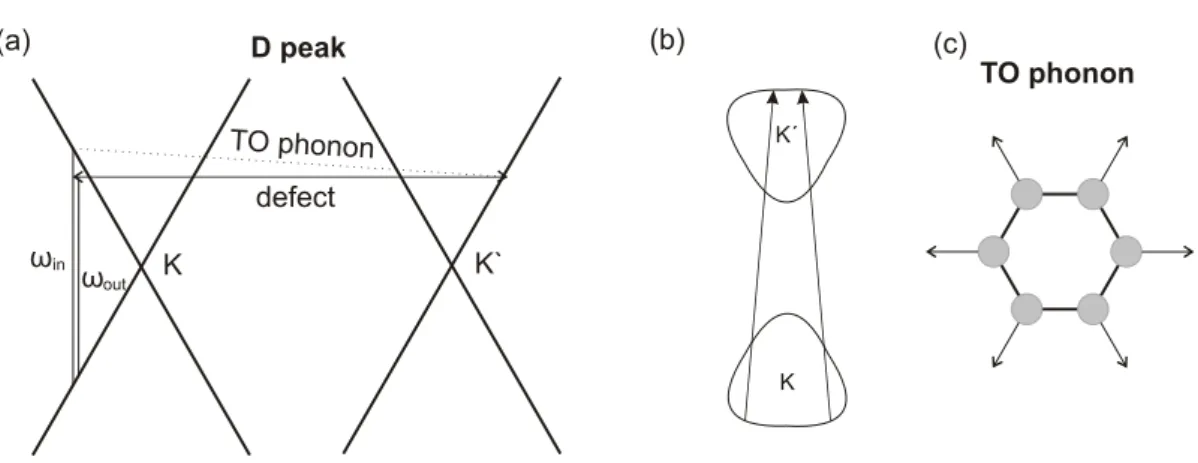
Another Raman feature in graphene is the D peak, whose position is sensitive to the excitation wavelength and is found around 1345 cm−1 when an excitation wavelength of 532 nm is used. It is caused by a double-resonant second-order Ra- man scattering process involving one TO phonon from around the K-point and thus is Raman-forbidden, requiring a defect for momentum conservation. Conse- quently, the D peak is only found at edges or other defect sites and is frequently used to determine the quality of a graphene ake. How the chirality of an edge inuences the D peak is discussed below. Fig. 3.7(a) shows one possible double- resonant intervalley scattering process contributing to the D peak. The D mode is dominated by phonons along the K−M line connecting the strongly curved part of the Dirac cone around K with the weakly curved section around K0, see Fig. 3.7(b). Contributions from phonons between Γ and K are weaker due to destructive interference [Nar08]. Contributions from phonons withq = K cancel completely [Nar08]. For more discussion of the issue, see also [Kür02], [Mau04a]
and [Fer06]. Fig. 3.7(c) shows a sketch of the lattice vibration associated with the TO phonon at the K point.
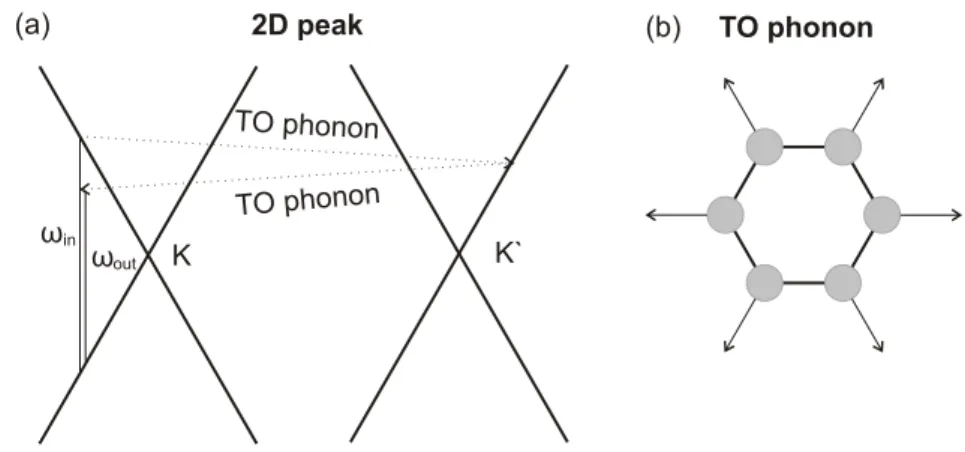
The second overtone of the D peak at about 2700 cm−1, called 2D peak, is depicted in Fig.3.8(a). It is, like the D peak, caused by a double-resonant inter- valley scattering process and its position is sensitive to the excitation wavelength.
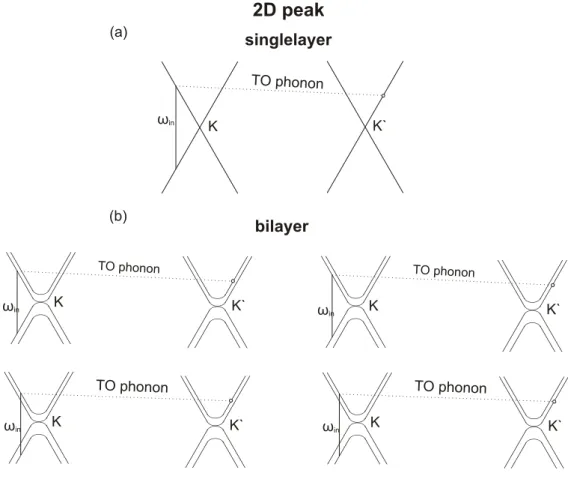
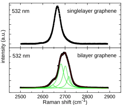
Since here two TO phonons with opposite momenta are involved, the fundamental Raman selection rule is always fullled and the 2D peak is allowed everywhere on graphene. In single layer graphene, the 2D peak appears as a single, sharp Lorentzian. In bi- and multilayer graphene, it changes shape and position, allow- ing for certain distinction of single- and bilayer graphene. This will be discussed below. Fig. 3.11(b) shows a sketch of the lattice vibration associated with the TO phonon at the K point.
Figure 3.10: double-resonant scattering process resulting in the 2D peak in (a) single layer and (b) bilayer graphene. For clarity, only one phonon is sketched.
The open circles denote points of resonance in the K0 valley. In single layer graphene, the 2D peak is dominated by one scattering process, resulting in a single, sharp Lorentzian. In bilayer graphene, four scattering processes dominate the 2D peak, resulting in four peaks which comprise the 2D peak in bilayer graphene and give it its characteristic shape.
Fig. 3.9 illustrates a double-resonant intra-valley scattering process involving a defect and an LO phonon, which results in the D0 peak at 1620 cm−1. Unlike the D peak, this mode does not depend on edge chirality.
For a review of all Raman modes in graphene and graphite, see e.g. [Fer13], [Mal09] and [Rei04], for more information on double-resonant scattering in graphene see, e.g., [Tho00], [Bas08] and [Ven11].
3.3. RAMAN SCATTERING IN GRAPHENE 21
s i n g l e l a y e r g r a p h e n e 5 3 2 n m
2 5 0 0 2 6 0 0 2 7 0 0 2 8 0 0 2 9 0 0
intensity (a.u.)
R a m a n s h i f t ( c m - 1 )
b i l a y e r g r a p h e n e 5 3 2 n m
Figure 3.11: 2D peak of mechanically cleaved single layer (top) and bilayer (bot- tom) graphene. Excitation wavelength 532 nm. In single layer graphene, the 2D peak appears as a single Lorentzian at 2667 cm−1, in bilayer graphene, it consists of four Lorentz peaks and is stiened with respect to its position in single layer graphene.
3.3.2 Inuence of the number of layers on the 2D mode
The 2D peak is caused by a double-resonant intervalley scattering process, as discussed above. This makes it especially sensitive to the shape of the electron dispersion. When comparing single layer and bilayer graphene, the electronic bands are strikingly dierent. The π and π∗ valence- and conduction bands split from one band in single layer to two bands each in bilayer graphene and they are no longer linear close to the Dirac point. This causes the 2D peak scattering process to split from one dominant process to four processes, as indicated in Fig.
3.10. In principle, the incoming light has four possibilities to couple the four bands resulting in eight scattering processes, but according to density functional theory (DFT), the indicated transitions between either the inner or the outer valence and conduction band around the same K point are much stronger than the other two connecting an inner and an outer band around the same K point [Fer06]. After the initial, resonant excitation of an electron-hole pair, the electron is scattered resonantly via a TO phonon to either the inner or the outer conduction band around the K0 point. This leads to four slightly stiened peaks comprising the 2D peak in bilayer graphene resulting in the characteristic peak shape shown in Fig. 3.11. A triple-resonant process, where both the electron and the hole are
Figure 3.12: (a)Possible scattering mechanisms at the edge of a graphene ake in real space. The wavelike red arrows indicate photons, the solid black lines tra- jectories of electron and hole, the dashed green line a phonon. i)At an atomically smooth edge, only backscattering of the electron and hole after normal incidence leads to radiative recombination of electron and hole. ii)Oblique incidence scatters electron and hole to dierent regions of the ake, no radiative recombination. iii)A disordered edge allows backscattering under oblique incidence to end in radiative recombination. Image from [Cas09b]. (b)Real space representation of a graphene ake with an armchair (upper) and zigzag (lower) edge. d~a and d~z indicate the wavevectors associated with armchair and zigzag edge, respectively. (c)Reciprocal space representation aligned compatibly to the real space in (b). The solid black arrow represents scattering via a TO phonon near the K point, the dashed arrows marked d~a and d~z denote the ~k-vector provided by an armchair or zigzag edge, respectively. Images (b) and (c) from [Pim07].
resonantly scattered into the valley around K0, is also possible, but not sketched here. The 2D peak is dispersive and thus its shape changes for dierent excitation wavelengths.
3.3.3 Inuence of edge chirality on the D mode
As mentioned above, here we will discuss the scattering mechanism giving rise to the D peak in more detail. The D band generally requires a defect to be activated, but the nature of this defect is also crucial to a successful Raman process.That is to say, not every defect contributes to the D peak, for example, armchair edges have a D peak, but zigzag edges do not. The D peak is forbidden at pure zigzag edges. Here, we will discuss why only armchair or disordered edges yield a defect suitable to activate the Raman D band and pure zigzag edges do not.
3.3. RAMAN SCATTERING IN GRAPHENE 23
The double-resonant scattering process resulting in the D peak (compare also Fig. 3.7(a)) begins with a resonantly laserexcited electron-hole-pair around the K point. Then the electron (or hole) is scattered by a TO phonon to a state on the Dirac cone around the K0 point and scattered back to a virtual state near the original valley via a defect, where it recombines radiatively with its residual hole (or electron). Steps two (scattering by phonon) and three (scattering by defect) may also be reversed in order. A triple-resonant process, where the electron (hole) is scattered by a TO phonon and the hole (electron) is scattered by a defect to the K0 valley where they recombine is also possible.
Considering a process which is not fully resonant, one intermediate step violates the energy conservation (eq.3.1) by the amount of the phonon energy ~ωD ≈ 170 meV. Hence the lifetime of the electron-hole pair and likewise the duration of the whole scattering process is limited by the uncertainty principle (eq. 3.6) to about 1/ωD ≈3fs. This time limit, together with the electron (hole) velocity v ≈ 1.1 × 10⁶ m/s ≈ 7.3 eV Å/~ (which is also the slope of the Dirac cones) gives a spatial extension of the process of v/ωD ≈4 nm.
Neglecting trigonal warping and assuming that valence and conduction band are perfectly symmetrical, the electron (hole) energy, measured from the Dirac point, is about ≈ ~ωL/2 where ~ωL is the laser energy. Neglecting the photon momentum, the k-vector of the electron (hole), measured from the K point, is k = /(~v). Then the electron (hole) can be seen as a wave packet of size
≈1/k =~v/≈0.6 nm.
Electron and hole are created in a region δl with ~v/ < δl < v/ωD. Consid- ering the uncertainty principle (eq. 3.6), momentum conservation holds up to δq ≈~/δl < /v. Electron and hole must therefore have approximately opposite momenta after creation, since the photon momentum is negligible. These con- siderations are also true for phonon emission and radiative recombination. This means that electron and hole have to meet in an area of sizeδlwith approximately opposite momenta in order to recombine radiatively and successfully complete the Raman process.
Therefore, two constraints are imposed on the double-resonant scattering process, namely, (1) the wavevector of the phonon ~q must connect the valleys around K and K0 to scatter resonantly and (2) at the end of the process, electron and hole must be in close vicinity to each other. Because photon momentum is very small, the electron (or hole), backscattered by the edge, must meet the edge at normal incidence in order to meet its counterpart, which is backscattered by a phonon, as illustrated in Fig. 3.12(a)i). Since momentum is conserved in an ordered edge, oblique incidence (see Fig. 3.12(a)ii) does not lead to a successful completion of the Raman process. This is only the case in disordered edges, where momentum is not conserved along the edge (Fig. 3.12(a)iii)).
Fig. 3.12(b) shows the momenta d~a, ~dz given by an armchair or zigzag edge, re- spectively. A possible scattering process associated with the D peak is illustrated
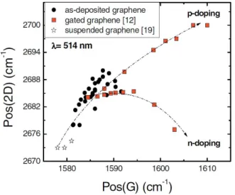
Figure 3.13: Position of the G mode versus position of the 2D mode. Data points marked by orange squares were taken on a gated single layer graphene sample. The correlation is nearly linear for p-type doping and strongly curved for n-type doping.
Graph taken from [Cas09a].
in Fig. 3.12(c). A TO phonon with wavevector ~q scatters the excited electron (hole) from a real state in the K valley to a real state in the K0 valley. From there it can only be backscattered into its original valley via d~a, the momentum given by an armchair edge. The momentumd~z given by a zigzag edge scatters the electron (hole) not along theK−K0 direction in the crystal but along theK0−K0 direction. In this scenario, the overall momentum in the scattering process is not conserved and zigzag edges do therefore not contribute to the Raman D band.
This does not touch the D0 peak. This peak is generated by an intra-valley scat- tering process, which can be sucessfully completed at both armchair and zigzag edges.
For experiments on this issue, see also [Can04], [Cas09b] and [Kra10].
3.3.4 Inuence of charge carriers on the G and 2D modes
The G peak is especially sensitive to a change in the charge carrier density in graphene and reacts quite strongly already to a small number of charges. Thereby it exhibits the same behavior for electron- as for hole-doping.
For electrically neutral graphene, the Fermi levelEF is at the Dirac point and the Kohn anomaly, which appears at 2kF [Koh59], in the doubly-degenerate optical phonon is exactly at theΓ-point since kF = 0. The Kohn anomaly is a softening of the phonon due to electron-phonon interaction. When EF is raised (lowered), the Fermi surface changes from a point to a circle and the value of the Fermi
3.3. RAMAN SCATTERING IN GRAPHENE 25
wavevector k~F increases from zero to a non-zero value. As the Kohn anomaly is coupled to k~F, it, too, moves away from k = 0([Koh59]) and the phonon stiens at the Γ-point. Consequently, the G peak, which probes the phonon dispersion at the Γ-point, stiens as the graphene changes from electrically neutral to doped.
According to [Yan07], [Pis07], [Das08] and the measurements presented in chap- ter 5.2, the G mode shifts by 1 cm−1 for every 4.5 x 1011 cm−2 charge carriers, starting at 1580 cm−1 for electrically neutral graphene.
While |EF| < ~ωG/2 where ωG is the angular frequency of the G mode, the G peak is Landau-damped [Yan07]. In this case, the G mode phonons can decay into electron-hole pairs. These are real transitions that conserve energy and momen- tum. Since G peak phonons have only small momentum, these must be almost vertical transitions with very small wave vector transfer. To satisfy the Pauli prin- ciple, such decay processes are only allowed if |EF|<~ωG/2 ≈ 100meV [Yan07].
This threshold corresponds to a charge carrier density of 1.1 x 1012 cm−2. In the Landau-damping regime, full width at half maximum (FWHM) of the G band is about 13 cm−1, outside it, FWHM is about 9 cm−1. Theoretically, the change in FWHM should be sudden, but in experiments it is observed as a gradual shift.
This is presumably due to charged impurities trapped in the substrate or arbi- trary, localized charges on the ake caused by self-doping [Per06], and chemical adsorption. Such disorder gives rise to electron-hole puddles in electrically neutral graphene, and allows the presence of local charge carriers even though the average charge carrier density vanishes [Mar08].
Although the TO phonon also exhibits a Kohn anomaly at the K point, the 2D peak associated with this phonon does not react as sensitively to small changes in charge carrier density as the G mode. However, when large amounts of electrons (holes) are introduced, it, too, begins to shift position, but asymmetrically for electron- and hole-doping, unlike the G mode.
For electron concentrations up to about 3 x 1013 cm−2, the position of the 2D mode remains nearly stagnant (shift < 1 cm−1, see [Das08]), then it softens. For hole-doping, the 2D band is unmoved until 5 x 1012 cm−2, then it stiens. A change in FWHM has not been observed in the literature.
This sensitivity of the position of both the G and the 2D mode to charge carriers and their dierent reactions toward electrons and holes make these Raman modes an ideal tool to identify amount and nature of doping in a ake. Plotting the position of the 2D band Pos(2D) via the position of the G band Pos(G) gives a characteristic shape and enables one to easily distinguish between electron- and hole-doping. The orange squares in Fig. 3.13 depict data points gathered on a gated ake, representing the change in position for n-type and p-type doping, respectively. If the ake is p-type doped, G peak and 2D peak move with almost constant shift, creating a nearly straight branch in the plot. For electron doping, the irregular behavior of the 2D peak leads to a downwards-bent branch for n-type doping.
For theoretical discussions of this topic, see [Pis04], [Laz06], [Net07] and [Bor10], for experiments, see [Yan07], [Pis07] and [Das08].
Chapter 4
Sample fabrication and experimental setup
This chapter introduces the samples discussed in this work and the preparation processes for both circular and hexagonal antidots. Finally, it describes the two measurement setups used in this work.
4.1 Sample fabrication and samples
In this work, one single layer ake with a backgate and two types of nanopatterned graphene akes were studied: graphene with circular antidots and graphene with hexagonal antidots.
4.1.1 General preparation of single layer graphene and sub- strate
All samples were prepared from natural graphite by the well-known mechanical cleavage method (e.g. [Nov05]) on heavily p-doped Si, capped by 300 nm SiO2, to allow backgating. The substrate is also tailored to allow easy identication of graphene akes in an optical microscope using white light. Graphene has a universal value of light absorption, πα = 2.3%, where α is the ne structure constant[Nai08]. Other two-dimensional semiconductors, like InAs nanomem- branes, have been found to have a step-like absorption. As the excitation energy is tuned, the absorptance increases in steps whose height is independent of the material thickness in the sample[Fan13]. The combination of graphene's signi- cant absorption and the interference aided by the transparent oxide layer of the
27
substrate, allows the detection of even single layer akes[Bla07]. However, if the thickness of the oxide layer is changed by only 5% to 315 nm, the contrast is signicantly lowered[Bla07]. Therefore, detection depends on the thickness of the oxide layer and the color of the illumination.
A similar eect is observed in the Raman modes of graphene on Si/SiO2 wafers.
Multiple Raman scattering events at the interfaces allows interference to alter the observed intensity of the Raman modes[Yoo09], making it dependent on both oxide layer thickness and the wavelength of the observed Raman light, which in turn depends on the excitation wavelength. This has only an impact on the inter- pretation of measurements, if the absolute intensity of a peak is considered or if intensities of dierent peaks or one peak measured with dierent excitation wave- lengths are compared. If one compares only intensities of one mode, measured with the same excitation wavelength, this has no implications.
All substrates are patterned with a gold alignment grid to allow easy access to pre-identied akes. With the exception of the gated ake, all samples were fabri- cated without contacts to avoid unintentional doping by vacuum deposited metal.
4.1.2 Single layer graphene with backgate
One otherwise unaltered single layer graphene ake was contacted and gated to allow tuning of the charge carrier density in the ake. The sample was prepared by Dr. Jonathan Eroms.
From transport experiments on similar samples, the applied backgate voltage (V) Vgate in this sample can be linked to the number of electrons n in the ake as n = 7.2 × 1010 cm−2 × (Vgate−VDirac) with VDirac the backgate voltage (V) necessary to shift the Fermi level to the charge-neutrality point.
The Fermi energy in graphene changes as EF(n) = ~|vF|√
πn with vF = 1.1 × 10⁶ m/s the Fermi velocity.
4.1.3 Single layer graphene with circular antidots
Four dierent graphene akes, each including a single layer part, were patterned with periodic arrays of circular holes, so-called circular antidots. The nanopat- tern was written on Polymethylmethacrylate (PMMA) resist using electron-beam lithography (EBL), after developping the resist, the antidots were etched by reac- tive ion etching (RIE) with oxygen as reactive gas. We prepared square antidot lattices with four dierent lattice constants ranging from 80 nm to 400 nm and two types of hole diameter, 50 nm and 60 nm. The samples are named circAD to indicate circular antidots, followed by the lattice constant in nm. If a distinction between larger and smaller hole diameters is necessary, the lattices with smaller antidots are denoted (s). If possible, the akes were left partially unpatterned to
4.1. SAMPLE FABRICATION AND SAMPLES 29
(a) 5 mm
100 nm (b)
(c) A
B R
Figure 4.1: (a) microscope image of sample circAD80. The dashed black rectangles indicate, where the ake has been patterned with circu- lar antidot lattices. (b), (c) scan- ning electron microscope images of areas B and A, respectively. Antidots in A have a slightly larger diameter (60 nm) than in B (50 nm).
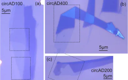
Figure 4.2: microscope images of sample (a) circAD100, (b) circAD400, and (c) circAD200. Black dashed rectangles mark which areas were etched with antidot lattices. (a) sample circAD100 has single- and bilayer, both with antidots and without as reference section. (b) sample circAD400 has a single layer area with antidots and an unpatterned reference area. (c) sample circAD200 has a small single layer area with antidots, but no single layer reference section.
provide a reference section on each sample.
All samples of this series are courtesy of Dr. Jonathan Eroms.
To evaluate the Raman data gathered on all EBL and RIE treated samples, it is necessary to take the inuence of EBL and RIE on Raman spectra in graphene into account. Reference [Fan11] nds, that spin-coating PMMA resist onto graphene results in a small amount of disorder in the ake, which is reected in the Raman spectrum in a D peak and a decrease in the G peak intensity. However, this dis- order, which is presumably caused by adsorbates, was found to resist an acetone bath but may be removed by annealing [Fan11]. Since the samples with circular antidots are not heated in the patterning process, there may be residual adsor- bates on the surface. The samples with hexagonal antidots (see below), however, are annealed in the etching process and should therefore not carry adsorbates caused by PMMA coating.
Figure 4.3: (a) microscope image of sample hexAD(200/400). The dashed black rectangles mark where the ake has been patterned with antidot lattices. Area A has a lattice constant of 400 nm, area B of 200 nm. Region R was left unpatterned as reference section. (b) phase contrast AFM image of the antidot lattice in area B after the second anisotropic etching step. Note the hexagonal shape of many antidots.
Sample circAD80 is a single layer graphene ake patterned with two lattices of circular antidots with 80 nm lattice constant, one lattice with 50 nm hole diame- ter, the other lattice with 60 nm hole diameter, and a reference section. Fig. 4.1 shows a microscope image and two scanning electron microscope (SEM) images of circAD80. The black rectangles mark where the ake was patterned. The an- tidots in area A have a slightly larger diameter (60 nm) than in B (50 nm).
Sample circAD100 consists of a single layer and a bilayer part. It was patterned with two antidot lattices with 100 nm lattice constant, one with 50 nm and one with 60 nm hole diameter. Both, in the single- and the bilayer region, a reference section was left unpatterned. For a microscope image of the ake with sketched antidot lattices, see Fig. 4.2(a). This ake will be introduced again in more detail in chapter 5.
Sample circAD200 has a small single layer area etched with antidots with 200 nm lattice constant and 60 nm hole diameter, but no single layer reference section.
Fig. 4.2(c) shows an image of the ake.
Sample circAD400 has a large single layer region patterned with an antidot lat- tice with 400 nm lattice constant and 60 nm hole diameter. Part of the single layer was left unpatterned, as may be seen from Fig. 4.2(b).
4.1. SAMPLE FABRICATION AND SAMPLES 31
4.1.4 Single layer graphene with hexagonal antidots
With care, it is possible to selectively etch carbon atoms located at specic edge sites. This bears the possibility to create devices where one type of edge chiral- ity greatly prevails. In the literature, two approaches to anisotropic etching can be found: One through catalysts, where metallic or non-metallic nanoparticles move along a graphene ake and etch trenches [Dat08], [Cam09], [Gao09], the other where pristine or prepatterned akes are subjected to heating in dierent atmospheres [NI10], [Yan10], [Shi11]. The advantage of the non-catalyzed form over the catalyzed one is that prepatterning of the akes allows position control over the edges and e.g. enables one to leave an unpatterned reference section, whereas the movements of the catalyst nanoparticles over the ake are, due to the distribution process of the nanoparticles, uniform and largely random. Only the angles between trenches favor 60◦ and 30◦, as a result of the graphene lattice.
Since reference sections were wanted, a non-catalyzed etching process was chosen for the sample presented in this work.
The sample was processed by Florian Oberhuber.
A graphene ake with a very large single layer part was prepared with two hexag- onal antidot lattices and a reference section. First, the ake was patterned with circular antidots with EBL and RIE, as described above. Diameter of the cir- cular antidots was 40 nm in both lattices. Then followed a preparation step in which the ake was heated in a quartz tube reactor with a stainless steel grid to change the chemical environment of the ake for the ensuing anisotropic etching step. The sample was then etched without the grid in the reactor at a temperature T ≈820 ◦C in a ow of Ar gas (purity ≥99.9999 %, O2 ≤ 0.5ppm) at ambient pressure. During this etching step, the circular antidots grow to hexagonal anti- dots, because not all atoms along the edge of each antidot are removed equally.
The aim is to predominantly etch atoms at armchair sites and consequently be left with antidots which have predominantly zigzag edges, creating the honeycomb outline of the antidots. This anisotropic etching step was then repeated once more. After the rst anisotropic etching step, antidot diameters were between 70 nm and 80 nm, after the second etching step, between 125 nm and 145 nm.
It is still speculative, how exactly the anisotropic etching comes to pass and why the preparation step is necessary for anisotropic etching in single layer graphene, but not in bi- or multilayer graphene [Obe13]. The best performance for anisotropic etching was found in a narrow temperature range around T 820◦C, with lateral etch rates≈ 20nm/h for single layer graphene [Obe13]. Reference [NI10] suggests that the etching reaction occurs between graphene and oxygen atoms from the SiO2-layer, however, Oberhuber et al. observed anisotropic etching in the top layers of multilayer graphene with intact bottom layers, insulating the etching site from the SiO2 [Obe13]. They suggest that the reaction involves gaseous O2
with concentrations ≤ 0.5 ppm in the Ar atmosphere, as an additional ow of H2 gas could inhibit the etch reaction [Obe13]. See especially the supplementary
camera
Laser CCD
camera
Laser CCD
(a) (b)
Figure 4.4: (a)Micro-Raman setup used to record spectra on the series of sam- ples with circular antidots. Excitation source was a 532 nm diode-pumped solid state laser. Samples were mounted on an x-y-stage with 100 nm minimal step size and spectra were recorded using a triple Raman spectrometer equipped with a liquid nitrogen-cooled CCD detector. (b)Micro-Raman setup used to monitor the evolution hexAD(200/400). Excitation source was a circularly polarized 532 nm diode-pumped solid state laser. Spectra were recorded using a single stage Ra- man spectrometer equipped with 1200 grooves per mm holographic grating and a thermoelectrically cooled CCD detector.
material to [Obe13] for details on this discussion.
Fig. 4.3(a) shows a microscope image of the sample. The dashed black rectangles indicate the etched areas of the ake. The lattice constant in area A is 400 nm and 200 nm in area B. Area R was left unpatterned as reference section. Fig.
4.3(b) shows an AFM image of part of area B with 200 nm lattice constant. The AFM image was acquired after the last Raman scan.
In this particular ake, its evolution was carefully monitored by Raman spec- troscopy, meaning that after each preparation step two scans of the ake were made. One scan monitored the D and G bands, the other the 2D band. No scan- ning electron microscopy (SEM) images were taken until after the nal Raman scan was completed to not contaminate the ake with charge carriers or impuri- ties.
This sample will be referred to as hexAD(400/200), since it has two antidot lattices with 400 nm and 200 nm lattice constant, respectively.
![Figure 3.4: (a) phonon dispersion of graphite (adapted from [Mau04b]). Solid lines are ab initio calculations, lled circles are experimental data gathered by in-elastic x-ray scattering, the dashed red line is a cubic spline connecting the experi-mental](https://thumb-eu.123doks.com/thumbv2/1library_info/5632525.1692895/21.892.122.717.241.783/figure-dispersion-graphite-calculations-experimental-gathered-scattering-connecting.webp)