Efficient gating of epitaxial boron nitride monolayers by substrate functionalization
A. Fedorov,
1,2,3,*C. S. Praveen,
4,*N. I. Verbitskiy,
1,5,6D. Haberer,
7D. Usachov,
3D. V. Vyalikh,
3,8A. Nefedov,
9C. W¨oll,
9L. Petaccia,
10S. Piccinin,
4H. Sachdev,
11M. Knupfer,
2B. B¨uchner,
2S. Fabris,
4,†and A. Gr¨uneis
1,‡1
II. Physikalisches Institut, Universit¨at zu K¨oln, Z¨ulpicher Strasse 77, 50937 K¨oln, Germany
2
Institute for Solid State Research, IFW Dresden, P.O. Box 270116, D-01171 Dresden, Germany
3
St. Petersburg State University, St. Petersburg 198504, Russia
4
Theory@Elettra Group, CNR-IOM DEMOCRITOS and SISSA, via Bonomea 265, 34136 Trieste, Italy
5
Faculty of Physics, University of Vienna, Strudlhofgasse 4, A-1090 Vienna, Austria
6
Department of Materials Science, Moscow State University, Leninskiye Gory 1/3, 119992 Moscow, Russia
7
Department of Physics, University of California at Berkeley, Berkeley, California 94720, USA
8
Institute of Solid State Physics, Dresden University of Technology, D-01062 Dresden, Germany
9
Institute f¨ur Funktionelle Grenzfl¨achen (IFG), Karlsruher Institut f¨ur Technologie (KIT), Hermann-von-Helmoltz-Platz 1, D-76344 Eggenstein-Leopoldshafen, Germany
10
Elettra Sincrotrone Trieste, Strada Statale 14 km 163.5, 34149 Trieste, Italy
11
Max-Planck-Institut f¨ur Polymerforschung, Ackermannweg 10, D-55128 Mainz, Germany (Received 15 May 2015; revised manuscript received 4 August 2015; published 28 September 2015) Insulating hexagonal boron nitride monolayers (hBN) are best known for being resistant to chemical functionalization. This property makes hBN an excellent substrate for graphene heterostructures, but limits its application as an active element in nanoelectronics where tunable electronic properties are needed. Moreover, the two-dimensional–materials’ community wishes to learn more about the adsorption and intercalation characteristics of alkali metals on hBN, which have direct relevance to several electrochemistry experiments that are envisioned with layered materials. Here we provide results on ionic functionalization of hBN/metal interfaces with K and Li dopants. By combining angle-resolved photoemission spectroscopy (ARPES), x-ray photoelectron spectroscopy, and density functional theory calculations, we show that the metallic substrate readily ionizes the alkali dopants and exposes hBN to large electric fields and band-energy shifts. In particular, if hBN is in between the negatively charged substrate and the positive alkali ion, this allows us to directly study, using ARPES, the effects of large electric fields on the electron energy bands of hBN.
DOI: 10.1103/PhysRevB.92.125440 PACS number(s): 73.22. − f
I. INTRODUCTION
Hexagonal boron nitride (hBN), a structural analog to graphene, has been attracting considerable research attention due to its outstanding mechanical properties, its potential for surface chemistry [1], and its potential applications in far-ultraviolet (far-UV) optoelectronic devices [2,3] and two- dimensional (2D) heterostructures comprising graphene and hBN [4,5]. First results on chemical functionalization of hBN have also been reported by trapping atoms or molecules on the dipole rings of epitaxial boron nitride [1]. The ionicity of the B-N bond induces a wide band gap in hBN with a direct optical transition for bulk hBN of about 5.9 eV [3,6,7].
The lack of electronic states at or close to the Fermi level also limits the chemical activity of hBN. In contrast to carbon materials, where ionic [8], covalent [9], and substitutional [10]
doping have been successfully carried out, the interaction of potassium with bulk hBN does not result in charge transfer to the electronic states of hBN [11] owing to the large energy band gap. This insulating and chemically inert behavior is exploited in novel 2D devices which use hBN as a substrate for graphene in order to attain high electronic mobilities. In such epitaxial hBN/graphene heterostructures, a small gap in
*
Authors contributed equally to this work.
†
fabris@democritos.it
‡
grueneis@ph2.uni-koeln.de
graphene is predicted [12] and the highest mobilities known for graphene are achieved [13]. But the lack of response to chemical functionalization severely limits the usefulness of hBN as an active element, which has prompted the search for alternative methods to manipulate its electronic properties.
In particular, the application of large electric fields leads to a giant Stark effect, which was theoretically predicted for hBN nanotubes [14] and hBN nanoribbons [15]. Experimental evidence of this, albeit only at the single-molecule level, was gathered by scanning tunneling spectroscopy (STS) measurements for tip-induced electric fields in the vicinity of a hBN nanotube [16]. Electric fields applied to hBN tubes with a controlled defect concentration are also the basis for a recently predicted gate-tunable light-emitting device [17]. Field effect transistors (FETs) based on hBN nanotubes exhibit a robust ON / OFF ratio [18]. The parent compounds of these systems are hBN monolayers [19–21] and hBN nanomeshes [22], which can be grown epitaxially in high crystallinity in areas exceeding 1 × 1 cm by chemical-vapor deposition (CVD) on metals. Recently, hBN was found to support space-charge-limited current, which is promising for UV-light-emitting diodes and laser diodes [23]. Despite the simple structure and the theoretical progress in understanding of the hBN band structure, little is known about the effects of gating and electric fields on their electronic properties.
This is a direct result of the fact that in order to apply a
homogeneous electronic gating, the hBN monolayer must be
transferred from the catalytic metal substrate to an insulator
and supplied with electric contacts. The resulting devices are usually too small [23] to be probed by angle-resolved photoemission spectroscopy (ARPES), which relies on large (i.e., in the mm range) single-crystalline materials.
Here we take a different approach by exposing hBN to the large potentials and electric fields generated by an intercalated or adsorbed layer of ionized alkali metal. This not only relieves us from the task of transferring hBN but also retains the large size and high crystallinity of the hBN layer, which allows us to directly probe the effects of the electric field on the electron energy band structure by ARPES. In addition, we employ x-ray photoemission spectroscopy (XPS) and near-edge x-ray absorption fine-structure spectroscopy (NEXAFS). These methods allow us to study the interface structure of the dopant/hBN system, i.e., whether the dopant preferably is above or under hBN, and to probe the unoccupied states, respectively. The crucial point in this approach is that hBN is on a Au substrate that readily ionizes the deposited alkali atoms, which is somewhat similar for doped graphene on metal substrates, where ARPES and density functional theory (DFT) have shown that a part of the electron charge is transferred to the metal [8,24]. The present case is different from the graphene case, in the sense that graphene accepts a large fraction of the alkali atom’s charge while hBN does not.
Our work, therefore, constitutes an experimental realization of chemical functionalization of an hBN/metal interface using alkali metals and its direct measurement using ARPES. The possibility to tune the electronic properties of hBN monolayers is also highly relevant to the field of novel hBN-graphene het- erostructures. We purposefully engineer hBN/potassium/Au and lithium/hBN/Au structures. DFT calculations reproduce the ARPES data and are used for their interpretation: These simulations show a clear relationship between the energy shift of the hBN electron energy bands and the presence of interfacial potential differences and electric fields induced by the alkali metals.
II. RESULTS
Figure 1(a) depicts the XPS measurements that show the B1s and N1s core levels for pristine and alkali-metal functionalized hBN. It is clear that both core levels exhibit a shift towards higher binding energy (BE) in the latter case.
This behavior is similar to graphene and graphite [8,24].
However, as we will show in the following, it is not due to a charge transfer but interfacial electric fields that yield potential differences between the substrate and hBN. We also observe a different shift for the N1s and B1s core levels. This can be ascribed to a combination of initial- and final-state effects originating from the charge reorganization at the hBN plane due to the dopant deposition.
It is notable that during all photoemission experiments, the hBN layer was not charging, i.e., the Au substrate forms a good electrical contact to hBN. As we will show later, this good contact is formed by a weak hybridization between hBN and Au.
Let us consider the XPS measurements of the alkali-metal core levels in more detail. Figure 1(b) depicts the angle- dependent XPS spectra of both the K2p and Li1s core levels.
The relative intensity ratio (normalized to the N1s core-level
FIG. 1. (Color online) (a) hBN core-level spectra measured by XPS for pristine and alkali-metal-dopedhBN. (b) Normal and grazing emission core-level spectra of the alkali metals. (c),(d) NEXAFS spectra for the N and B K edges, respectively, for pristine and alkali- metal-doped hBN.
intensity) indicates the preferred location of each species (either above or below the hBN plane) [24]. As a result, we obtain a preference of K to intercalate in between hBN and Au/Ni(111) and a preference of Li to adsorb on top of hBN.
We note that this behavior is identical to K and Li interaction with graphene on Au/Ni(111) [24]. We speculate that the different behavior for various alkali metals stems from the preference of some of them to form surface alloys while others do not.
In order to probe the effects of the alkali ions on the con-
duction band of hBN, we performed NEXAFS measurements.
This technique probes the transitions from N1s and B1s core levels to the unoccupied π
∗and σ
∗states and gives information about the hybridization of the electronic states. No extra peaks appear in the NEXAFS spectrum upon doping, but for both, pristine and doped hBN, a small shoulder is present in the N1s edge when compared to bulk hBN, as reported earlier [25]. In the present case, this shoulder is much weaker since the interaction between hBN and Au is weaker than the interaction between hBN and Ni. Nevertheless, it allows us to conclude that the hBN is weakly interacting with the substrate.
This weak interaction is also evident from the ARPES data via a hybridization and is crucially important for the effects described below since it allows us to treat the metal-hBN interface as one system with a common Fermi energy and work function.
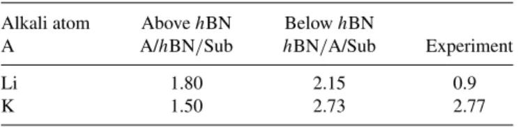
Let us focus now on the band structure modifications. In Fig. 2, the ARPES scan along the K high-symmetry direction in the 2D Brillouin zone (BZ) of hBN for pristine as well as Li- and K-doped samples is presented [Figs. 2(a)–2(c)]. Similar to the core levels of hBN, the π band shifts down after alkali deposition. In the case of K, the downshift is 2.77 eV, while for the Li case, it is 0.9 eV. The large downshift in the case of K doping brings the top of the π band in the vicinity of the Au5d bands, allowing a weak hybridization which can be seen as a loss of photoemission intensity in the band-crossing regions in the top of the π band [Fig. 2(d)]. Concomitant with the NEXAFS results, this small hybridization highlights that the hBN/Au interface must be treated as one coupled, weakly interacting system. The anticrossing in the σ bands of hBN is analyzed in Fig. 2(e). The energy-dispersion curves through the K point in the region of the anticrossing are shown for pristine and doped hBN on Au. It can be seen that for Li doping, the anticrossing persists, while K doping removes the anticrossing in the σ bands at K. This behavior is consistent with the suggested position of Li on top of hBN and the intercalation of K in between the hBN/Au interface. In the case of K intercalation, the hBN layer is lifted up and so the interaction of the in-plane σ orbitals with the substrate is removed. Moreover, we observe a strong reduction of ARPES intensity at the Fermi level due to the K intercalation, which suppresses the Fermi-level photoemission intensity dominated by Au orbitals due to the smaller inelastic mean free path in the K layer. The fact that, after K intercalation, hybridization with Au appears in the π bands despite the larger distance between hBN and Au can be understood by the matching energies of π and Au5d levels and by the larger extent of the π orbitals in the z direction compared to the σ orbitals which lie in the hBN plane. In the case of Li doping, the hybridization of states at the π-band maximum at the K point and Au5d is not possible since their energies do not match.
We now turn to a discussion of the qualitative reason for the observed downshifts of the hBN electronic bands before a quantitative description using DFT. The driving force behind these observed changes is the interaction of the Au substrate with the alkali atom. This can lead to the combined effects of gating via a potential and electric fields acting on hBN.
In particular, since the K atoms are readily ionized by the Au substrate, hBN is exposed to an electric potential which is able to shift its electronic band structure. The same effect will occur for Li/hBN/Au but, due to its sandwichlike structure where
TABLE I. Energy shifts of the π bands in the functionalized systems where the alkali atom (A) is above (A/hBN/Au) or below (hBN/A/Au) the hBN sheet. The energy shifts are expressed in eV and are relative to the top of the hBN π band in the pristine BN/Au system.
Alkali atom Above hBN Below hBN
A A/hBN/Sub hBN/A/Sub Experiment
Li 1.80 2.15 0.9
K 1.50 2.73 2.77
hBN is in between Li
+and Au
−, there is an additional electric field between the ionized Li atom and the Au surface present.
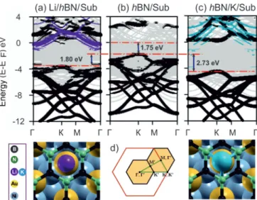
Performing DFT calculations, we find that the actual energy shift of the hBN bands depends on many factors, most notably the coverage of the Li and K dopants, as well as their position with respect to the hBN layer. The calculations were performed by assuming the same coverage of 1/8 monolayer with respect to the honeycomb layer for both Li and K. Although this choice may not represent the actual experimental conditions, it provides a valuable insight into the effects of the two dopants on the BN/Sub system, removing the effects of different dopant coverage. Concerning the position of the dopant, we consider different locations of the Li and K dopants at the interface, namely, above and below the hBN layer. We refer to these four cases as Li/hBN/Sub, hBN/Li/Sub, K/hBN/Sub, and hBN/K/Sub, where “Sub” indicates the Au/Ni substrate. The summarized results of the corresponding π-band energy shifts are shown in Table I: alkali atom intercalation always yields the largest shifts. This is because the interaction with the metal substrate facilitates the charge transfer, which consistently leads to the charge of the intercalated ions being ∝2× larger than the corresponding one of the adsorbed ions. From a comparison of the theoretical to the experimental ARPES values, it can be concluded that the systems that yield a band-energy shift most compatible with the experiment are those in which K intercalates while Li adsorbs on the upper surface of hBN, which is also in agreement with the angle- dependent XPS data. For these systems, the calculated hBN band shifts referred to the top of the hBN π band in the pristine hBN/Au system are 1.80 eV for Li/hBN/Sub and 2.73 eV for hBN/K/Sub. In Fig. 3, we report the atom-projected band structures calculated for the 2 × 2 unit cell. The energy shift of the hBN π band (black lines) in the functionalized systems is almost rigid and is experienced by all of the hBN-derived bands. For the K case, the calculated value of the hBN π-band shift (2.73 eV) is in very good agreement with the ARPES data (2.77 eV), thus indicating that the coverage considered in the model supercells is compatible with the one of the measured sample. In the case of Li, the calculations overestimate the hBN band shift (1.80 eV) with respect to the measured value (0.9 eV). We attribute this to the following reason. To make the calculations feasible (smaller unit-cell size), we fixed the in-plane dopant superstructure to be 2 × 2 for both dopants.
For the case of K, this superstructure was experimentally verified for bulk hBN [11]. However, in the case of carbon materials, Li is known to form a √
3 × √
3 superstructure and
nothing is known of its adsorption pattern on hBN. Although
FIG. 2. (Color online) ARPES spectra along the K high-symmetry direction of the hexagonal BZ for (a) pristine hBN on Au, (b) Li functionalized hBN on Au, and (c) K functionalized hBN on Au. The K point is at 1.7 ˚ A
−1. (d) A zoom of the π -band maximum for K-doped hBN close to the K point. (e) Energy-dispersion curves through the σ bands along the dotted lines. The Fermi-level position of the Au substrate is defined as zero.
we could not perform calculations with √ 3 × √
3 Li coverage, increasing the Li coverage to 1/4 ML yielded larger shifts by
∼25%. This therefore suggests that a better agreement with the experiment would be obtained with lower Li coverage, which therefore better represents the experimental conditions.
Indeed, the saturation limit detected by ARPES for Li doping can originate from the fact that neutral Li clusters form that do not contribute to the charge-transfer reaction. Such clusters are equivalent to a diluted atomic Li coverage in the calculations.
This assumption is strongly supported by the fact that we observed a Li
0component in the XPS spectrum at a dosage of about 1/4 ML (see Supplemental Material [26]). For this Li coverage, however, the ARPES-derived band structure was not affected. Since Li has a very small photoemission cross section and the resolution of XPS is limited, the signal from smaller quantities of partially ionized or neutral Li clusters
FIG. 3. (Color online) (a)–(c) DFT-calculated atom-projected band structures of alkali-metal functionalized hBN on Au/Ni (Ni:
gray; hBN: black; Li: purple; K: blue). The thickness of the lines varies according to the contribution of each atomic state at that particular energy. A sketch representing the top view of the respective functionalized systems is shown in the bottom panel of (a) and (c).
(d) Folding of the 2 × 2 BZ with respect to the 1 × 1 zone.
can be undetectable. In summary, the observed shift for Li qualitatively agrees with the experiment in both cases and is in very good quantitative agreement with the case of K.
We now move to the analysis of the optimized geometry and to the charge distribution resulting from the DFT calculations.
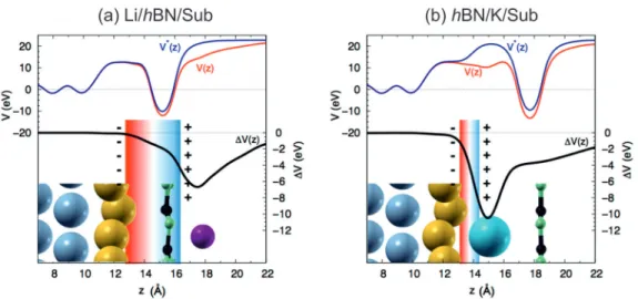
The bottom panel of Fig. 3 displays the top view of the simulated unit cells. The side view is shown in the inset of Fig. 4. Alkali functionalization induces structural distortions and relaxations to the reference hBN/Au lattices. In the case of K, the distance between the metal substrate and the hBN sheet increases from 3.05 ˚ A to 5.41 ˚ A. In this configuration, the plane of the K atoms is 2.53 ˚ A above the metal and 2.88 ˚ A below the hBN sheet, while in the case of Li, the dopants are predicted to be 1.90 ˚ A above the hBN sheet. In addition, this dopant induces an out-of-plane distortion of the hBN honeycomb lattice, with the N and B atoms relaxing outwards and inwards, respectively, resulting in a corrugation of 0.25 ˚ A. The corrugation of the hBN lattice predicted for the Li/hBN/Sub system resembles the polarization of an ionic honeycomb lattice subjected to a transverse electric field. It is due to the polar character of the B-N bond that leads to partial negative/positive excess charges on the N/B atoms. Conversely, the fact that a negligible lattice corrugation of 0.04 ˚ A is predicted for the hBN/K/Sub case suggests that the hBN sheet is exposed to a very small effective transverse electric field when the dopant is below the hBN plane. In addition, the rigid shift of the hBN π band is also consistent with a dopant-driven electric field at the interface. The following analysis of the potential across the interface allows us to identify these effective fields that modify the structural and electronic properties of the functionalized hBN/Au systems.
Starting from the Li case, we report in Fig. 4 the planar
average of the total Kohn-Sham (KS) potential along the z
direction of the Li/hBN/Sub supercell, V (z) (red line). For
further analysis, we construct a model reference substrate from
the Li/hBN/Sub supercell by removing the Li atom, while
leaving the coordinates of all other atoms unaltered. From here
onwards, we refer to this auxiliary system as hBN/Sub
and
notate the corresponding potential V
BN/Subas V
(z) in Fig. 4
(blue line). The average potential in the Ni slab is taken as
the zero reference for V (z). The difference V (z) = V (z) −
V
(z) is an approximation for the effective potential acting
FIG. 4. (Color online) DFT-calculated planar average of the total Kohn-Sham potential along the z direction of the supercell plotted for (a) Li/hBN/Sub and (b) hBN/K/Sub. The blue [V
(z)] and red [V (z)] lines shows the respective potential of the auxiliary substrate and the functionalized system (see text for the details of the notation). V (z) represents the effective potential due to the presence of the substrate. The capacitor is indicated by a box with red-blue gradient.
on the system due to the dopant (black line in Fig. 4). V is zero in the region of the metal support, while there is a drop between the Au and Li planes, leading to an effective potential of 1.95 eV at the hBN plane. This additional potential is responsible for the energy shift of the hBN π bands due to Li. There is, however, a small discrepancy between the value of this shift (1.95 eV) and the corresponding one resulting from the band structure calculation (1.80 eV; see Fig. 3). This originates from the different reference substrates that are used in the two analyses, hBN/Sub
and hBN/Sub.
1Most interestingly, the above analysis shows that the hBN plane is within a capacitorlike linear potential profile along the z direction [Fig. 4(a)]. Indeed, the binding of Li above the hBN sheet drives a charge reorganization, giving rise to δ
+and δ
−net charges at the Li and Au layers, respectively. This charge redistribution effectively generates an interface capacitor and a related effective field, which embeds the dielectric hBN plane, and therefore rigidly shifts its π bands. Quite consistently, the ionic hBN lattice responds to this effective field by a polarized structural distortion, i.e., the lattice corrugation described above.
The same analysis applied to the K case [Fig. 4(b)] shows the presence of an effective capacitor at the Au/K interface.
The important difference between the two cases is the position of the hBN plane with respect to this capacitor: inside the interfacial capacitor in the case of Li and outside it in the case of K. As such, the hBN is not directly subjected to an effective field in the hBN/K/Sub system and therefore the effective potential profile (V ) at the hBN plane is essentially constant. The interface effective field and the related capacitor introduce a potential difference at the hBN plane with respect
1