Lecture 5: Combination Lock
G. Kemnitz ∗ , TU Clausthal, Institute of Computer Science May 25, 2011
For a verbal target function of a combinatorial lock a state graph has to be designed. The state graph has next to be described in VHDL, simulated, embedded in a surrounding circuit, downloaded in the programmable circuit and tested.
1 Functional description and simulation
The circuit to be designed in this section should have a clock signal, an initial signal and a vector of 8 switch signals as inputs and the following LED outputs: a 4-bit signal to display the index of the next digit to be entered, a bit for error and a bit for accepted:
entity ZS_CombLock is port(Clk: in std_logic ;
sw: in std_logic_vector (7 downto 0);
Init: in std_logic ;
led_Z: out std_logic_vector (3 downto 0); -- index of next digit
led_err, led_acc: out std_logic ); -- bits for error and accepted end entity;
Pushing the initial button should re-initiate the state machine. The digits has to be entered by switching the corresponding switch on and off. If the correct switch is turned on and off, the control should move to the next »good« state else if a wrong or multiple switches are turned on and off it should be move to the next »bad« state. In each case the index of the next digit to be entered should be displayed. After entering the last number, if all numbers have been correct, the output »accepted« and otherwise the output »error« should be activated. The four correct digits should be declared as 8-bit constants. The final states in which the output »led_err« or
»led_acc« is activated, should be left only by pressing the initialization button. During pressing the initialization button all LEDs should be off.
1. Draw the state graph on the handout sheet.
2. Design an architecture to the given entity withe the main functionality in a sampling process.
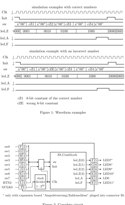
3. Design a testbench for simulation, to test the design unit » ZS_Automat « with the waveforms in figure 1.
4. Add an input waveform in which temporally two switches are turned on to check that also those switch sequences are interpreted as incorrect.
2 The complete circuit and its test
The design unit from the section before should be embedded in the circuit in figure 2. For de- bouncing the whole circuit should run with a clock frequency of approximately 50 Hz produced
∗
Tel. 05323/727116
1
by a clock divider. All input signals from switches and the initialization signal have to be sampled before they can be used by the internal function. The given LED to package pin assignments assumes, that the expansion board »Ampelsteuerung/Zahlenschloss
1« is pluged into connector
»B1«.
1. Describe the complete circuit in VHDL with the design unit »ZS_CombLock« developed in section before as an instance.
2. Program it into the FPGA on the test board and test it.
3 Check list for the compliance test
Exercise 1:
• State graph on the handout sheet.
• Presentation of the simulation result close to that in figure 1 plus a simulation sequence with two switches temporary turned on.
Exercise 2:
• Presentation of the final circuit.
1
Ampelsteuerung – engl. traffic light control; Zahlenschloss – engl. combinatorial lock
2
10
10 10 10 10
10 10 10
x”00” cZ1 x”00” x”00” cZ3 x”00” cZ4 x”00”
1000
0001 0010 0100
led A led Z sw Init Clk
led F
0000 0001 0000
cZE
simulation example with an incorrect number
cZ1 cZE
8-bit constant of the correct number wrong 8-bit constant
x”00” cZ1 x”00” cZ2 x”00” cZ3 x”00” cZ4 x”00”
1000
0001 0010 0100
led A led Z sw Init Clk
led F
0000 0001 0000
simulation examples with correct numbers
Figure 1: Waveform examples
1 : 2
20divider clock
GCLK0 T9
L14 F12 G12 H13
K14 K13 J13 J14 H14
sw7 BTN3
sw6 sw5 sw4 sw0 sw1 sw2 sw3
H16 K16 E15 K12 G16
F15 LED7
∗LED9
∗LED10
∗LED11
∗LED8
∗LD0 led Z(0)
led Z(1) led Z(2) led Z(3) led A led F Clk
Init sw
∗