Shot Noise Induced by Nonequilibrium Spin Accumulation
Tomonori Arakawa,1,* Junichi Shiogai,2 Mariusz Ciorga,3 Martin Utz,3 Dieter Schuh,3 Makoto Kohda,2,4 Junsaku Nitta,2 Dominique Bougeard,3 Dieter Weiss,3 Teruo Ono,5 and Kensuke Kobayashi1,†
1Department of Physics, Graduate School of Science, Osaka University, 1-1 Machikaneyama, Toyonaka, 560-0043 Osaka, Japan
2Department of Materials Science, Tohoku University, 980-8579 Sendai, Miyagi, Japan
3Institute of Experimental and Applied Physics, University of Regensburg, D-93040 Regensburg, Germany
4PRESTO, Japan Science and Technology Agency, 332-0012 Kawaguchi, Saitama, Japan
5Institute for Chemical Research, Kyoto University, 611-0011 Uji, Kyoto, Japan (Received 16 May 2014; published 7 January 2015)
When an electric current passes across a potential barrier, the partition process of electrons at the barrier gives rise to the shot noise, reflecting the discrete nature of the electric charge. Here we report the observation of excess shot noise connected with a spin current which is induced by a nonequilibrium spin accumulation in an all-semiconductor lateral spin-valve device. We find that this excess shot noise is proportional to the spin current. Additionally, we determine quantitatively the spin-injection-induced electron temperature by measuring the current noise. Our experiments show that spin accumulation driven shot noise provides a novel means of investigating nonequilibrium spin transport.
DOI:10.1103/PhysRevLett.114.016601 PACS numbers: 72.25.Dc, 72.15.Lh, 72.25.Hg, 73.40.Ty
In 1918, Schottky argued that the electric flow in a vacuum tube fluctuates in a unique way such that the spectral density of the fluctuations is proportional to the unit of chargee(e >0) and to the mean current[1]. This is the shot noise, the direct consequence of the discreteness of the electron charge. Now, as an electron possesses not only charge but also spin, one may ask how the discreteness of electron spin affects the current fluctuations. Although such spin-dependent shot noise has been discussed theo- retically in various contexts [2–11], it has never been evidenced experimentally.
Recently it was pointed out that a nonequilibrium spin accumulation, which can be generated, e.g., by electrical spin injection, modifies the current noise spectrum and allows measurement of the magnitude of the spin accu- mulation electrically[11]. While Meairet al.explore in this theoretical work the noise measured between different contacts of a mesoscopic cavity with and without non- equilibrium spin accumulation, we analyze here noise measured across a tunneling barrier where one of the contacts carries a nonequilibrium spin accumulation while the other is in equilibrium [see inset of Fig.1(a)]. Assuming a linearI-Vcharacteristic of the device, the current spectral densitySis forΔμ¼0proportional to the applied voltage Vdue to shot noise. For finite spin accumulation, however, Sis forT ¼0given byS∝jeVþΔμ=2j þ jeV−Δμ=2j.
This means that atV ¼0the noise density is finite. Plotted as a function of V, the spin accumulation appears as a plateau of widthΔμ=e, shown in Fig. 1(a). Finite temper- atures will smear out the pronounced kinks at Δμ=2e. Using instead of an unpolarized contact in thermal equi- librium a ferromagnetic one offers even more options to measure the spin accumulation electrically, as is pointed
out below. In the case of a ferromagnetic contact, the expression forSgets modified and reads
S↑=↓∝αjeVΔμ=2j þβjeV∓Δμ=2j: ð1Þ Here α and β (α>β) define the ratio of the tunnel conductances of majority and minority spins (αþβ¼1), and ↑=↓ denotes the spin direction with respect to the magnetization of the detector contact. The resultingSðVÞ relation is plotted in Fig. 1(b). In addition to the kinks at Δμ=2e, the spin-up and spin-down noise density is horizontally shifted byγΔμ=e, whereγ is the spin asym- metry coefficient given byγ ¼α−β. Below we denote the vertical shift ofS↑andS↓as excess shot noise, correspond- ing to the noise which is entirely generated by the spin accumulation.
In this Letter we demonstrate the validity of the concepts presented above by measuring shot noise across a tunneling
(b)
S (arb. unit)
V (mV)
-1 0 1
=0
-1 0 1
=0 V (mV)
/e /e
(a)
S (arb. unit)
/e
L R
eV
S S
R
FIG. 1 (color online). (a) Current noise at T¼0 for Δμ¼400μeV, when a nonmagnetic detector electrode is used [11]. The inset shows the schematic energy diagram. The dotted curve indicates shot noise without spin accumulation. (b) Current noise when a ferromagnetic contact is used on one side of the tunneling barrier as a detector electrode (α¼0.75andβ¼0.25).
barrier in the presence of spin accumulation. By using a ferromagnetic detector electrode, we have successfully extracted the relation between the spin current and the corresponding excess shot noise, and we have found that the estimated Fano factor directly shows that the spin degree of freedom is preserved in the tunneling process.
Given the importance of shot noise in various fields, especially in device technology [12] and mesoscopic physics [13–15], excess shot noise due to spin accumu- lation could not only serve as a unique probe to explore the spin-dependent nonequilibrium transport process but also to shed new light on the recently emerging field of spin noise spectroscopy[16–19].
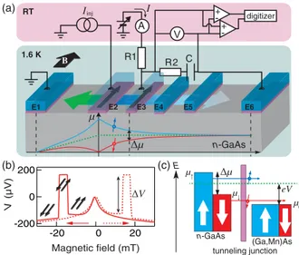
A spin accumulation can be generated, e.g., by electrical spin injection [20,21]. To this end, we prepared a lateral all-semiconductor spin-valve device, which was fabricated from a single epitaxial wafer grown by molecular beam epitaxy on a (001) GaAs substrate, consisting of, in the growth order, a GaAs buffer, an AlGaAs/GaAs superlattice, a 1μm n-GaAs channel, a 15 nm GaAs with linearly graded doping n→nþ (n¼2×1016 cm−3 and nþ¼ 5×1018 cm−3), an 8 nm nþ-GaAs, a 2.2 nm AlGaAs, and a 50 nm (Ga0.945Mn0.055) As. Because of the highnþ- doped GaAs region adjacent to the degeneratelyp-doped (Ga,Mn)As layer, a tunneling Esaki diode structure is formed at the junction, enabling efficient generation and detection of spin accumulation in n-GaAs. The wafer was patterned into 50μm—wide mesas along the [110]
direction by standard photolithography and wet chemical etching. Then six ferromagnetic (Ga,Mn)As electrodes (E1 toE6) are defined by electron beam lithography and by wet chemical etching down to the lightly dopedn-GaAs channel, as schematically shown in Fig.2(a) [22–24]. Each ferromagnetic electrode serves a specific purpose: one is used as an injection electrode (E2), three as detection electrodes (E3,E4, andE5), and two as reference electro- des (E1andE6). Only the E1 electrode is grounded.
By applying a constant currentIinjtoE2[see Fig.2(a)], we inject spin polarized electrons into then-GaAs channel.
As a consequence, spin accumulation—i.e., splitting of the chemical potentials (Δμ¼μ↑−μ↓) for spin-up and spin-down electrons (μ↑ and μ↓, respectively)—occurs underneath the injection contact and diffuses to both sides.
Figure 2(b) shows a typical spin accumulation signal obtained by measuring the nonlocal dc voltage difference between contactsE3andE6as a function of the in-plane magnetic field B[see Fig. 2(a)]. All of the measurements were carried out at 1.6 K in a variable temperature insert.
The abrupt voltage changes, displayed in Fig.1(b), corre- spond to magnetization switching of E2 or E3. Different coercive fields were adjusted by different widths of the respective contacts. The voltage change ΔV between parallel (P) and antiparallel (AP) magnetization configu- rations, being 0.30 mV here, is proportional to Δμ and
given byΔV¼γΔμ=e[25,26]. For our device we extract γ¼0.820.03in the smallIinj limit[22,24].
To measure Sthrough the tunneling barrier formed by the Esaki diode at the p-(Ga,Mn)As/n-GaAs interface at the corresponding contact, we use an additional circuit, as shown in Fig.2(a). Three passive components are placed at 1.6 K: two surface mounted metal-film resistors (R1¼1MΩ,R2¼1kΩ) and a laminated ceramic capaci- tor (C¼1μF). S is converted to voltage noise by R2, while R1 prevents the current noise from leaking to the voltage source. The two sets of voltage noise signals are independently amplified by two amplifiers (NF LI-75A) at room temperature and are recorded at a two-channel digitizer. Cross-correlation spectra were obtained in the frequency range between 16 kHz and 160 kHz (9001 points)[27,28]. To extractSacross the tunneling barrier, we carefully calibrated the measurement system and elimi- nated thermal noise from R2 and the channel resistance [24]. We experimentally confirmed that the contribution of frequency-dependent noise, such as 1=f noise, does not affectSfor the parameter range examined.
The measurement procedure is as follows[24]: together with the constant spin injection current Iinj, which determines the manitude of the spin accumulation, we inject a small currentIto one of the detection electrodes
1.6 K
A
digitizer
B RT
E1
R1 R2 C
I
E2 E3
V (V)
Magnetic field (mT)
n-GaAs
n-GaAs
(Ga,Mn)As eV E
(a)
) c ( )
b (
-+ -+
-200 0 200
-20 0 20
E4 E5 E6
0
tunneling junction
inj I
FIG. 2 (color online). (a) Schematic diagram of the sample and measurement system. Six (Ga,Mn)As electrodes (E1toE6) are placed on then-GaAs channel, whereE2(4μm ×50μm size) is an injection electrode, while either E3, E4, or E5 (0.5μm×
50μm size) is a detection electrode. The center-to-center spacing between the neighboring electrodes is5μm. Schematic spatial dependence of each chemical potential in then-GaAs channel is illustrated. (b) Typical nonlocal voltage signal forIinj¼−23 μA.
A peak observed around the zero magnetic field is induced by dynamic nuclear spin polarization (DNP) [23]. This effect is irrelevant to the present result, as the noise measurement was performed outside of the DNP region. (c) Schematic energy diagram at the detection electrode in the presence ofeVandΔμ.
(eitherE3,E4, orE5) using a constant current technique [see Fig. 2(a)]. We directly measure the voltage drop V andSacross the tunneling barrier, as schematically shown in Fig.2(c). The dependence of these values on currentI was measured for both P and AP configurations. Note that by reversing the contact magnetization we switch the up and down direction of the accumulated spins in the n-GaAs channel. As I is set between −300nA and 300 nA, well belowIinj, the influence of this probe current on the spin accumulation is negligibly small. The data shown in Fig. 3(a) are obtained for injection currents Iinj¼0;−9, and −23μA atE3. In order to compare our data with the predictions of Eq.(1), we discuss below the measured noiseSas a function ofV. For Iinj¼0 μA, the observed Sis independent of the magnetization configu- ration, and it monotonically increases as jVj increases, as expected from conventional shot noise theory [13].
The finiteSatV ¼0stems from thermal noise. This curve is perfectly reproduced by the conventional formula given by
S¼4kBTe
Rd
þ2F
eIcoth
eV
2kBTe
−4kBTe
Rd
; ð2Þ
whereRd,Te, andFare the differential resistance at a given bias, the electron temperature, and the Fano factor, respec- tively. For Te¼1.6K, the fitting to this formula gives F¼0.780.04, as shown in Fig.3(a)by the dotted curve.
The Fano factor is slightly reduced from unity, as expected for a tunneling junction. This is most probably due to the contribution of defects in the tunneling barrier which are unavoidably created during the (low-temperature) growth process[29–31].
WhenIinj is finite, i.e., for−9and−23μA, Sstarts to depend on the magnetization configuration, as expected by Eq.(1)except for the low bias region, which is dominated by thermal noise [See Figs.1(b)and3(a)]. Moreover, for Iinj¼−23μA, the horizontal shift ofSbetween P and AP configurations is 0.28 mV, matching closely the magnitude of the nonlocal voltage signal ofΔV ¼0.30mV, shown in Fig. 1(b). This indicates the validity of the scenario put forward in the introduction and demonstrates that “noise spectroscopy”successfully detects the nonequilibrium spin accumulation Δμ [see also Fig. 2(c)]. We emphasize that the observed difference between the two different magnetic configurations is reproducible. Actually, theBdependence of S was measured for a constant V ¼−6.8mV in independent measurements, as shown in Fig. 3(b). Clear spin-valve-like changes were observed for Iinj ¼−9μA and −23μA, reflecting magnetization switching in the electrodes, while no detectable change was observed for Iinj¼0μA. Thus, the configuration-dependent contribu- tion of the noise measured at finiteIinj is undoubtedly the shot noise associated with spin accumulation.
In order to distinguish contributions from the voltage drop across the barrierVand the spin accumulation in the channelΔμin the measured current, we adopt the following model based on the Landauer-Büttiker formalism[13,32].
Currents for P (IP) and AP (IAP) states are written as IP=AP ¼e
hT1ðeVΔμ=2Þ þe
hT2ðeV∓Δμ=2Þ; ð3Þ with T1ð2Þ being the sum of all of the transmission probabilities of the tunneling channels from the nonmag- netic GaAs conduction band states to the majority (minor- ity) spin states in the ferromagnetic (Ga,Mn)As. The first and second terms in Eq. (3) represent tunneling currents with up- and down-spin, respectively. By using the ratio of the tunneling conductances, α¼T1=ðT1þT2Þ and β¼T2=ðT1þT2Þ, Eq. (3) can be rewritten as IP=AP¼ ð2e=hÞTeV¯ ðe=hÞðα−βÞTΔμ, where¯ T¯ ≡ðT1þT2Þ=2.
To separate the currents driven by the applied biasV and the spin accumulation Δμ, we define the charge current IC≡ð2e=hÞTeV¯ and the spin current IS≡ðe=hÞTΔμ¯ . Note that this spin current is solely driven by the spin
40
0 S (10-27 A2 /Hz)
-5 0 5
V (mV)
55
50
45
Magnetic field (mT) S (10-27 A2 /Hz)
) b ( )
a (
IS (nA) -23 µA
-9 µA -23 µA -23 µA
5 µm 5 µm 10 µm 15 µm
(c)
4
2
00 10 20 30
80
40
00 300
S (10-27 A2 /Hz)S S (10-27 A2 /Hz)C
IC (nA)
C 2 C
S = eI F
S 2 S
S = eI F
E2 E3
-20 -15
sweep -23 µA AP P
-9 µA AP P 0 µA AP P
fitted
Iinj L
Iinj
20 60
FIG. 3 (color online). (a) MeasuredSat E3 as a function of V for P and AP configurations for several injection currents.
The curves are offset vertically by1×10−26 A2=Hz for clarity.
The dotted curve is the fitted curve from Eq.(1). The error bar for each point is 0.4×10⁻²⁷ A2=Hz. (b) B dependence of S measured with keeping V constant (V¼−6.8mV) for Iinj¼0;−9, and−23μA (from bottom to top). The thick arrows denote the magnetization directions ofE2andE3. (c)SSversus ISfor the bias region (jeVj>Δμ=2,2kBT) for several injection currents and for different detection electrodes. The dashed line is the linear relation withF¼0.77. The inset shows the counterpart of the main graph forSC versusIC.
accumulation in the n-GaAs channel. These currents can be extracted from the experiment using the relations, hICi ¼ ðIPþIAPÞ=2 and hISi ¼ ðIP−IAPÞ=2ðα−βÞ. By using the experimentally obtained value of γ, we deter- minedαandβ as 0.91 and 0.09, respectively. The energy dependence of these values is negligible in the present experiment at low bias.
We first focus on the excess shot noise in the high bias region (jeVj>Δμ=2,2kBT) and discuss the measured noise in parallel configuration SP and antiparallel configuration SAP. Note that, becausejeVj>Δμ=2, eithereVΔμ=2>
0 or eVΔμ=2<0 holds [see Fig. 2(c)]. By similar transformations, SP and SAP can be written as SP=AP¼ ð4e2=hÞTFeV¯ ð2e2=hÞðα−βÞTFΔμ. Accordingly, the¯ conventional shot noise SC and the excess shot noise SSare defined asSC≡ð4e2=hÞTFeV¯ ¼ ðSPþSAPÞ=2and SS≡ð2e2=hÞTFΔμ¯ ¼(jSP−SAPj=2ðα−βÞ), respectively.
Using experiments such as the one shown in Fig. 2(a), we can experimentally derive the relation betweenhISiand SS exactly as in conventional shot noise experiments. By tuningIinj, choosing different electrodes for detection (E3, E4, or E5), or both, we perform noise measurements for different values of Δμ. In Fig. 3(c), we show the corre- sponding dataSSvshISiandSCvshICiforjeVj>Δμ=2, 2kBT, for several values of Iinj and for different detec- tion electrodes. SC is well fitted by the linear function SC¼2eFjhICij [see inset in Fig. 3(c)], which yields F¼0.770.04, consistent with the zero-injection case discussed above [see Fig.3(a)]. Similarly, we find that the excess shot noise SS also linearly depends on hISi and, more importantly, satisfies the relation SS¼2eFjhISij (dashed line) with the same Fano factor obtained for the conventional shot noise. Both the linear relations and the equal Fano factors justify the applied procedure to extract the excess shot noise which is generated by the spin accumulation.
In the low bias region (jeVj≤Δμ=2), SP and SAP are expected to have opposite slopes, as shown in Fig.1(b). For finite temperature, the pronounced kinks at V¼ Δμ=2e are smeared, and Eq. (1) need to be replaced by S↑=↓∝ αjeVΔμ=2jcoshððeVΔμ=2Þ=2kBTeÞ þβjeV∓Δμ=2j coshððeV∓Δμ=2Þ=2kBTeÞ. For an electron temperature of Te ¼1.6K, equal to the bath temperature, the kinks should be detectable[11]. However, this structure is not resolved in experiments due to the thermal smearing of the distribution function by the injected hot electrons.
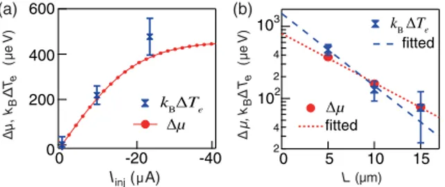
The latter can be seen by estimating the degree of nonequilibrium in terms of the effective electron temper- ature by fitting ðSPþSAPÞ=2 to Eq. (2). The estimated value ofkBTe is always larger thanΔμ.kBΔTeandΔμare plotted againstIinjand the injector-detector separationLin Figs.4(a)and4(b), respectively, whereΔTe(≡Te−1.6K) is the effective temperature rise. One can see that, as Δμ increases as a function of Iinj,kBΔTe increases similarly.
To the best of our knowledge, direct information such as
kBΔTeto characterize the degree of nonequilibrium due to spin accumulation has not been demonstrated so far.
Moreover, asΔμ relaxes according to the diffusion equa- tion,kBΔTealso relaxes. By fittingΔμandkBΔTetoΔμ∝ expð−L=λSÞand kBΔTe∝expð−L=λeÞ, we obtain a spin relaxation length λS¼5.6μm and an energy relaxation length λe ¼4.3μm in the channel, respectively [see the dashed curves in Fig.4(b)]. The good agreement between the two relaxation lengths indicates that spin relaxation is accompanied by energy relaxation.
Finally, we note that the SC andSS described here are identical due to the absence of spin flips [2,4,8,10] or Coulomb interaction effects [6], which would otherwise generate different Fano factors for spin and charge current.
By measuring this difference, general spin-dependent shot noise physics can be addressed. In addition, the present demonstration can lead to a new probe to explore the spin- transfer torque physics[9], the spin heat accumulation[33], and the spin-dependent chiral edge states in topological insulators[34].
In summary, we have shown that a nonequilibrium spin accumulation can be detected in the noise spectrum includ- ing the distribution function. The Landauer-Büttiker formal- ism allowed us to disentangle conventional shot noise associated with the charge current and excess shot noise, connected with a spin current. However, because of the elevated electron temperature stemming from nonlocal spin injection, it was not possible to explore excess shot noise in the limit V→0, i.e., when only a pure spin current is flowing.
We appreciate the fruitful comments and support from M. Ferrier and R. Sakano. This work is partially supported by a Grant-in-Aid for Scientific Research (S) (Grant No. 26220711) from JSPS, a Grant-in-Aid for Scientific Research on Innovative Areas“Fluctuation and Structure” (Grant No. 25103003) from MEXT, and a Grant-in-Aid for Young Scientists (Start-up) (Grant No. 25887037) from JSPS, the Murata Science Foundation. D. W. and J. N.
acknowledge support from the German and Japanese Joint Research Program, the German Science Foundation (DFG) via SFB 689, and the Collaborative Research Program of the Institute for Chemical Research, Kyoto University.
µ, kT (µeV)
Iinj ( A) L ( m)
e
(a)
-40 0
600 400 200
0 0 5 10 15
2 4
B
103
102 (b)
fitted
kB Te fitted
kB Te
2 4
-20
kT (eV)eB
FIG. 4 (color online). (a) Iinj dependence of the extracted kBΔTe and Δμ at detector E3. (b) L dependence of kBΔTe
andΔμ forIinj¼−23μA.
*arakawa@phys.sci.osaka‑u.ac.jp
†kensuke@phys.sci.osaka‑u.ac.jp
[1] W. Schottky,Ann. Phys. (Berlin)362, 541 (1918).
[2] E. G. Mishchenko,Phys. Rev. B68, 100409 (2003).
[3] W. Belzig and M. Zareyan, Phys. Rev. B 69, 140407(R) (2004).
[4] A. Lamacraft, Phys. Rev. B69, 081301(R) (2004).
[5] B. Wang, J. Wang, and H. Guo,Phys. Rev. B69, 153301 (2004).
[6] O. Sauret and D. Feinberg, Phys. Rev. Lett. 92, 106601 (2004).
[7] J. Foros, A. Brataas, Y. Tserkovnyak, and G. E. W. Bauer, Phys. Rev. Lett.95, 016601 (2005).
[8] R. L. Dragomirova and B. K. Nikolić, Phys. Rev. B 75, 085328 (2007).
[9] A. L. Chudnovskiy, J. Swiebodzinski, and A. Kamenev, Phys. Rev. Lett.101, 066601 (2008).
[10] R. L. Dragomirova, L. P. Zârbo, and B. K. Nikolić, Europhys. Lett.84, 37004 (2008).
[11] J. Meair, P. Stano, and P. Jacquod,Phys. Rev. B84, 073302 (2011).
[12] S. M. Sze and K. K. Ng,Physics of Semiconductor Devices (John Wiley & Sons, New York, 2007).
[13] Ya. M. Blanter and M. Büttiker, Phys. Rep. 336, 1 (2000).
[14] Quantum Noise in Mesoscopic Physics, edited by Y. V.
Nazarov (Kluwer, Dordrecht, 2003).
[15] C. W. J. Beenakker and C. Schönenberger,Phys. Today56, No. 5, 37 (2003).
[16] S. A. Crooker, D. G. Rickel, A. V. Balatsky, and D. L.
Smith,Nature (London)431, 49 (2004).
[17] M. Oestreich, M. Romer, R. J. Haug, and D. Hagele,Phys.
Rev. Lett.95, 216603 (2005).
[18] S. A. Crooker, J. Brandt, C. Sandfort, A. Greilich, D. R.
Yakovlev, D. Reuter, A. D. Wieck, and M. Bayer,Phys. Rev.
Lett.104, 036601 (2010).
[19] A. V. Kuhlmann, J. Houel, A. Ludwig, L. Greuter, D. Reuter, A. D. Wieck, M. Poggio, and R. J. Warburton, Nat. Phys.9, 570 (2013).
[20] F. J. Jedema, A. T. Filip, and B. J. van Wees, Nature (London) 410, 345 (2001).
[21] X. Lou, C. Adelmann, S. A. Crooker, E. S. Garlid, J. Zhang, K. S. Madhukar Reddy, S. D. Flexner, C. J. Palmstrøm, and P. A. Crowell,Nat. Phys. 3, 197 (2007).
[22] M. Ciorga, A. Einwanger, U. Wurstbauer, D. Schuh, W.
Wegscheider, and D. Weiss,Phys. Rev. B79, 165321 (2009).
[23] J. Shiogai, M. Ciorga, M. Utz, D. Schuh, T. Arakawa, M.
Kohda, K. Kobayashi, T. Ono, W. Wegscheider, D. Weiss, and J. Nitta,Appl. Phys. Lett. 101, 212402 (2012).
[24] See Supplemental Material at http://link.aps.org/
supplemental/10.1103/PhysRevLett.114.016601 for addi- tional data and discussion.
[25] A. Fert and H. Jaffrès,Phys. Rev. B64, 184420 (2001).
[26] S. Takahashi and S. Maekawa,Phys. Rev. B 67, 052409 (2003).
[27] A. Kumar, L. Saminadayar, D. C. Glattli, Y. Jin, and B. Etienne,Phys. Rev. Lett.76, 2778 (1996).
[28] T. Arakawa, K. Sekiguchi, S. Nakamura, K. Chida, Y. Nishihara, D. Chiba, K. Kobayashi, A. Fukushima, S. Yuasa, and T. Ono,Appl. Phys. Lett.98, 202103 (2011).
[29] R. M. Feenstra, J. M. Woodall, and G. D. Pettit,Phys. Rev.
Lett.71, 1176 (1993).
[30] T. Tsuruoka, N. Tachikawa, S. Ushioda, F. Matsukura, K.
Takamura, and H. Ohno,Appl. Phys. Lett.81, 2800 (2002).
[31] A. Richardella, P. Roushan, S. Mack, B. Zhou, D. A. Huse, D. D. Awschalom, and A. Yazdani,Science327, 665 (2010).
[32] S. Datta, Electronic Transport in Mesoscopic Systems (Cambridge University Press, Cambridge, England, 1997).
[33] F. K. Dejene, J. Flipse, G. E. W. Bauer, and B. J. van Wees, Nat. Phys.9, 636 (2013).
[34] M. Z. Hasan and C. L. Kane, Rev. Mod. Phys. 82, 3045 (2010).