Tasks
Today 23.09 Peierls Transitions & Charge Ordering Tomorrow 24.09 Guest Lecture Christof Aegerter
Monday 30.09
Tasks: Kramer-Kronig Transforms
Read: Kittel, Chapter: Optical Processes and Excitons Three Smaller Notes – On the website
Hand-in exercise sheet Tuesday 01.10
Tasks: Excitons
Read: Kittel, Chapter: Optical Processes and Excitons
Planning
Today 23.09 Peierls Transitions & Charge Ordering Tomorrow 24.09 Guest Lecture Christof Aegerter
Monday 30.09
Tasks: Presentation of Pascal (20 min + 5 min discussions) Kramers-Kronig Transforms
Read: Kittel, Chapter: Optical Processes and Excitons Three Smaller Notes – On the website
Hand-in exercise sheet Tuesday 01.10
Tasks: Excitons
Read: Kittel, Chapter: Optical Processes and Excitons Flipped class room activity:
Short Conceptual Presentation:
What does causality mean?
What is a response function?
What can be said about the Kramers-Kronig relations?
Derivation of KK-relations:
Use causality to derive KK-relations.
See hand written notes
2-5 min presentation:
Anar or Nik?
20-25 min presentation:
Nora?
Implications of KK-relations:
Why is the KK-relations useful?
Examples:
Harmonic oscillator Optical experiments
30 min presentation:
Johan?
Bechgaard Salts
beta-co-(BEDT-TTF)2I3
CRYSTAL STRUCTURE
J. Phys.: Condens. Matter 25 (2013) 343201
Bechgaard Salts
RESISTIVITY
J. Phys.: Condens. Matter 25 (2013) 343201
Bechgaard Salts
- Oxides –Perovskites (2D)
- Transition Metal Dichalcogenides (2D)
Charge ordering – Materials
- Organic Bechgaard Salts (1D)
TWO-DIMENSIONAL SYSTEMS
Dichalcogenides:
Examples
MoS 2 NbSe 2 IrTe 2 TaS 2
..
..
Crystal Structures
Niobium –diselenide:
NbSe 2
Niobium –diselenide:
NbSe 2
Ta Se 2
Nature Materials 7, 960 (2008)
- Oxides –Perovskites (2D)
- Transition Metal Dichalcogenides (2D)
Charge ordering – Materials
- Organic Bechgaard Salts (1D)
Oxides
La 2-x Sr x NiO 4
La 2-x Sr x CoO 4
La 2-x Sr x CuO 4
Nature Communications 7, 11632 (2016)
Different types of charge order
Charge stripe order
Checkerboard order
Nature Communications 7, 11632 (2016)
Different types of charge order
E. Fradkin & S. A. Kivelson
Nat. Phys. 8, 864 (2012) https://www.bnl.gov/newsroom/news.php?a=1865
John Tranquada et al., Nature 375, 561 (1995)
La 2-x Ba x CuO 4
Cuprates: Stripe order
- Kohn Anomaly: Spectroscopy
- New lattice modulation: X-ray diffraction
How to observe – charge ordering
- Charge modulation: STM
- Fermi Surface Reconstruction: Hall effect
- Fermi Surface Reconstruction: ARPES
IrTe 2
Nature Communications 6, 7342 (2015)
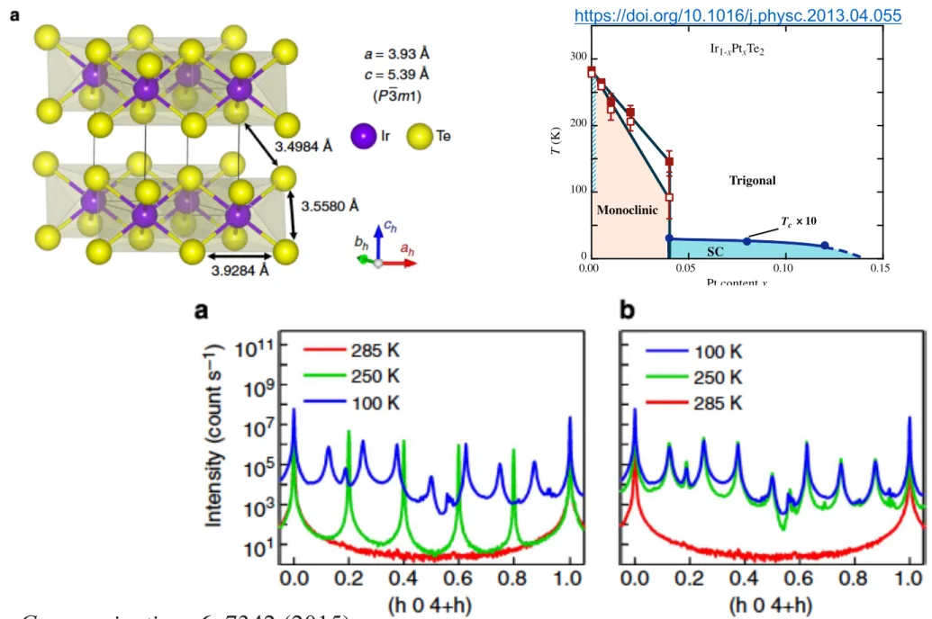
withx= 0.04 (#1 and #2) show an intriguing difference. The resis- tivity inx= 0.04 (#1) shows a steep jump around 90 K and a drop at 140 K. The temperature range of hysteresis is similar to that of polycrystalline Ir0.97Pt0.03Te2(x= 0.03). In contrast, the resistivity in x= 0.04 (#2) shows no hysteresis. The resistivity in x= 0.08, 0.12 also show no hysteresis. The resistivity behaviours of both x= 0.04 (#1) and (#2) indicate that the structural phase transition is completely suppressed at the nominal concentration ofx= 0.04 in the single crystal. This is largely consistent with the case of polycrystalline Ir1!xPtxTe2, where the structural phase transition is suppressed by Pt substitution at the critical content of xc= 0.035[1].
A superconducting transition appears in these samples. As shown inFig. 3a, a clear superconducting transition in the resistivity is observed for bothx= 0.04 (#2) and 0.08 at 3.1 K and 2.6 K, respec- tively. In contrast, the resistivity forx= 0.04 (#1) only shows a slight
decline. The resistivity of this batch shows clear hysteresis as shown inFig. 2a. This suggests that superconductivity emerges only when the structural phase transition is completely suppressed. This is consistent with the result of specific heat measurements in poly- crystalline Ir1!xPtxTe2, which show that bulk superconductivity emerges whenxis larger thanxc= 0.035[1]. Reductions in resistiv- ity in the parent compound of IrTe2(x= 0.0) may be caused by an ex- cess of Te [6]. The resistivity in the over-doped crystal (x= 0.12) does not decline above 1.8 K.Fig. 3b shows the low-temperature magnetization in the Ir1!xPtxTe2single crystal. The weights of the measured samples are almost 1–3 mg. The samples ofx= 0.04 and 0.08 show diamagnetism onsets at 3.1 K and 2.6 K, respectively.
The sharp declines of magnetism in these samples suggest a homo- geneous Pt content in the samples. Under-doped samples do not show superconductivity. The over-doped sample (x= 0.12) shows a slight decline in magnetization below 2 K.
We also found a broad hysteresis of magnetization in a wide range of temperatures in pure IrTe2.Fig. 4shows the temperature dependence of magnetic susceptibility in Ir1!xPtxTe2single crys- tals. The structural transition temperature Ts can also be deter- mined from magnetic measurements [3]. A decrease in paramagnetic susceptibility at a structural transition can be under- stood as a reduction in the density of state, which is also suggested from optical measurements and NMR [6,8]. A magnetization of 06x60.04 shows a steep drop, which indicates the monoclinic- trigonal structural phase transition. No hysteresis is observed for x= 0.08 and 0.12. The estimated Tsis slightly higher than that in a previous report of polycrystals[1]. Forx= 0.0, two types of hys- teresis are observed. A sharp hysteresis around 280 K is consistent with that of the resistivity as shown inFig. 2a. A broad hysteresis in the temperature range between 100 and 280 K is observed. The magnetization of polycrystalline IrTe2shows only a single broad hysteresis[3]. This may indicate some kind of lattice instability in this temperature region. Previous electron or X-ray diffraction measurements have been performed around 84 and 80 K, respec- tively[2,3]. Further structural studies between 100 K and 280 K are needed.
The obtained results are summarized in the electronic phase diagram presented inFig. 5. By using Pt doping as a system-con- trolling parameter, the structural phase-transition temperature in IrTe2is reduced, and a new superconducting phase emerges. The bulk superconductivity appears forxP0.04, with a maximumTc
of 3.1 K at x= 0.04, after which Tc decreases with increasing x.
Superconductivity disappears forx> 0.12. This phase diagram ade- quately reproduced the previously reported diagram using poly- crystals. This suggests that Ts and Tc in IrTe2 can be systematically changed by Pt substitution using our method.
4. Conclusion
Ir1!xPtxTe2 single crystals with 0.006x60.12 were success- fully synthesized and characterized. The monoclinic phase is sup- pressed and disappears with slight Pt doping to the Ir site. The breaking of Ir–Ir bonds, a characteristic of the monoclinic phase in pure IrTe2is accompanied by the emergence of a superconduc- ting phase. The Pt-content dependence of the structural phase transition temperature andTcin single crystals adequately repro- duced those in polycrystalline crystals. We also found a broad hys- teresis of magnetization in a wide range of temperatures only in pure IrTe2. This hysteresis may be independent of the hysteresis that indicates the monoclinic-trigonal structural phase transition.
Acknowledgements
A portion of this work was performed at the Advanced Science Research Center, Okayama University. The work was partially
χ(a.u.)
300 200
100 0
T (K) Ir1-xPtxTe2
0.00 0.005 0.01 0.02 0.04 0.08
x= 0.12 H = 5 T
Fig. 4.Temperature dependence of magnetization in Ir1!xPtxTe2when applying a field of 5 T.
Ir1-xPtxTe2
Tc SC
300
200
100
0
T (K)
0.15 0.10
0.05 0.00
Pt content x Monoclinic
Trigonal 10
Fig. 5.Phase diagram of Ir1!xPtxTe2. Closed and open squares respectively represent Ts upon heating and cooling for Ir1!xPtxTe2. Closed circles represent theTcfor Ir1!xPtxTe2. SC represents the bulk superconducting phase. Hatched area represents a temperature range of broad hysteresis in resistivity.
S. Pyon et al. / Physica C 494 (2013) 80–84 83
https://doi.org/10.1016/j.physc.2013.04.055
www.nature.com/scientificreports/
4
SCIENTIFIC REPORTS | 7: 17157 | DOI:10.1038/s41598-017-16945-7
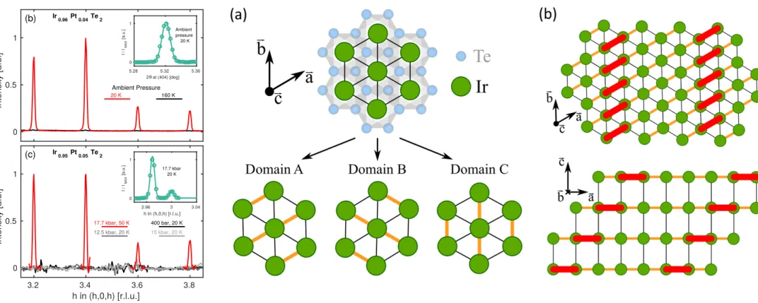
develops three domains with a short lattice parameter along the → a , →
b or → − → a b axes, see Fig. 3(a). All three types of domain are observed when scanning along the (1, 0, 1) direction in the pressure-induced twinned phase and hence two Bragg peaks are found – shown in Fig. 2(a). This twinning effect clearly appears before charge ordering, suggesting that the latter is lattice driven. Given that we observe the same (1/5, 0, 1/5) modulation as in IrTe
2(high-temperature), it is not inconceivable that the same conclusion applies to the parent compound.
Combining our results with previous studies of IrTe
2, we propose in Fig. 4(a) a schematic pressure, Pt substitution and temperature phase diagram including the charge ordering and the structural hexagonal to monoclinic transition.
Charge order structure. The surface and bulk charge ordering structure of IrTe
2has been studied by scanning tunnelling microscopy (STM)
29–34and x-ray diffraction
24,25,35techniques. The STM studies generally find uniaxial charge ordering structures. Furthermore, differences in charge modulations between the bulk and Figure 3. (a) Projection of the hexagonal crystal structure of IrTe
2. The transition into monoclinic structure implies formation of three domains where a short lattice parameter axis is found along the → a , →
b or → − → a b direction. These domains are labeled A, B and C respectively. (b) Stripe charge order forms along the short axis direction. The Ir
3+- Ir
3+dimers – indicated by red bonds – intersect the crystal structures with →
b , → a + → c planes.
Figure 4. (a) Schematic pressure - temperature phase diagrams of the charge ordering and crystal lattice twinning of Ir
1−xPt
xTe
2. (b) Hydrostatic pressure vs temperature map of the difference between the warming and cooling resistivity curves of Ir
0.95Pt
0.05Te
2represented in false colours. (c) Similar map but for the difference of each resistivity curve with the one measured at 1.4 kbar in the superconductor transition temperature range (displayed in logarithmic-intensity scale). Red ticks indicate the measured pressures. White dashed lines are guides to the eye.
www.nature.com/scientificreports/
3
SCIENTIFIC REPORTS | 7: 17157 | DOI:10.1038/s41598-017-16945-7
compared to the stoichiometric compounds IrTe2 and Ir3Te8 [Fig. 1(f)]. Empirically, it seems that the supercon- ducting transition broadens dramatically in the coexistent regime.
To gain further insight into the relation between the lattice and charge order, we carried out an x-ray diffrac- tion study. In Fig. 2(a), we show the fundamental lattice Bragg peak τ = (1, 0, 1) measured at low temperature on Ir0.95Pt0.05Te2 at different pressures as indicated. At low pressure (p = 400 bar) a single sharp Bragg peak is observed. Above a critical pressure pc1, this peak develops a shoulder that upon further increased pressure evolves into a separate Bragg peak. When heating above 200 K, this Bragg peak splitting disappears. Altogether, this evi- dences a low-temperature pressure-induced lowering of the lattice symmetry.
Next, we explore the charge ordering. Q-scans recorded on Ir0.96Pt0.04Te2 along the (h, 0, h) high symme- try direction are displayed in Fig. 2(b). Just as reported in IrTe224,25, no twinning was observed on Bragg peaks equivalent to τ = (1, 0, 1) – see inset. Moreover, below 160 K strong charge order reflections are observed at wave vectors Q =τ + qco where qco= (±1/5, 0, ±1/5) and (±2/5, 0, ±2/5) and τ are fundamental Bragg reflections. We find (not shown) that off-diagonal reflections of the type (h, 0, h + n) with n = 1, 2, 3 are much weaker than for n = 0. As the diffracted intensity I is proportional to Q · u where u is the atomic displacement27,28, we conclude that displacements are predominately along the (h, 0, h) direction.
With this knowledge, we studied the charge order in the pressure-induced twinned phase of Ir0.95Pt0.05Te2. The crystal was carefully aligned on the τ = (3, 0, 3) Bragg peak using the larger lattice constant. At the highest applied pressure p 17 7 kbar, a q. co = (±1/5, 0, ±1/5) charge modulation is observed with respect to the Bragg peak with the shorter lattice parameter [see Fig. 2(c)]. The charge ordering reflection displays, just as the resistivity curves, hysteretic behaviour as a function of temperature [inset of Fig. 2(e)]. Finally, we show in Fig. 2(e) how upon cooling the charge order reflection and the short-axis Bragg peak τ = (4, 0, 4) have identical temperature dependence. This demonstrates an intimate relation between the crystal lattice symmetry breaking and charge ordering.
Discussion/Interpretation
Lattice vs electronic mechanism. We start by discussing the nature of the charge ordering transition. The pressure-induced Bragg peak splitting [Fig. 2(a)] is most naturally explained in terms of domain formation caused by a lowering of the crystal lattice symmetry. In essence, our experiment suggests that the lattice parame- ters along the (1, 0, 1) and (0, 1, 1) directions become inequivalent under application of pressure. The system thus Figure 2. Lattice and charge ordering reflections in Ir1 – xPtxTe2. (a) Bragg peak (1, 0, 1) reflection measured in Ir0.95Pt0.05Te2 as a function of pressure as indicated. Solid lines are Gaussian fits to the data. (b) Ambient pressure x-ray diffracted intensity measured on Ir0.96Pt0.04Te2 along the (1, 0, 1) direction for 20 K (red line) and 160 K (black line) respectively. (c) Scan as in (b) but measured at base temperature (20 K) on Ir0.95Pt0.05Te2 for pressures as indicated. The slightly worse signal-to-noise level stems from the necessary background subtraction of signal originating from the pressure cell. (d) Bragg peak splitting and charge ordering intensity – shown in (a) and (c) – as a function of pressure. (e) Temperature dependence of the intensity of charge ordering and short- axis reflections on Ir0.95Pt0.05Te2 with maximum applied pressure, as indicated. Warming and cooling intensities of charge ordering are shown in the inset.
Charge Ordering in IrTe 2
1
SCIENTIFIC REPORTS | 7: 17157 | DOI:10.1038/s41598-017-16945-7
www.nature.com/scientificreports
Charge-Stripe Order and
Superconductivity in Ir 1 − x Pt x Te 2
O. Ivashko 1 , L. Yang 2,3 , D. Destraz 1 , E. Martino 2 , Y. Chen 4 , C. Y. Guo 4 , H. Q. Yuan 4 , A. Pisoni 2 , P. Matus 2 , S. Pyon 5 , K. Kudo 6 , M. Nohara 6 , L. Forró 2 , H. M. Rønnow 3 , M. Hücker 7 , M. v.
Zimmermann 8 & J. Chang 1
A combined resistivity and hard x-ray diffraction study of superconductivity and charge ordering in Ir Ir 1 − x Pt x Te 2 , as a function of Pt substitution and externally applied hydrostatic pressure, is presented.
Experiments are focused on samples near the critical composition x c ~ 0.045 where competition and switching between charge order and superconductivity is established. We show that charge order as a function of pressure in Ir 0.95 Pt 0.05 Te 2 is preempted — and hence triggered — by a structural transition.
Charge ordering appears uniaxially along the short crystallographic (1, 0, 1) domain axis with a
(1/5, 0, 1/5) modulation. Based on these results we draw a charge-order phase diagram and discuss the relation between stripe ordering and superconductivity.
Transition-metal dichalcogenides have long been the centre of considerable attention because of their complex quasi two-dimensional electronic properties. Semiconductor physics 1 , superconductivity 2–4 and spontaneous breaking of lattice symmetry, driven by charge-density waves (CDW) 5–7 , are commonly reported. Often, the ground state properties of these materials can be controlled by external non-thermal parameters such as chemical substitution 8 , magnetic field 9,10 or hydrostatic pressure 11 . The prototypical 1T-TaS 2 compound can, for example, be tuned from a CDW state to superconductivity by application of hydrostatic pressure 11 . Recently, a connection between charge density wave order in 1T-TaS 2 and orbital textures has been demonstrated 12 . A parallel effort has been to study dichalcogenide systems in which spin-orbit coupling is considerable. To this end, IrTe 2 has attracted interest because spin-orbit coupling on the Ir site is known to be large 13,14 . The IrTe 2 system displays high-temperature charge ordering, and superconductivity can be induced by Pt or Pd substitution that in turn quenches the charge order 15–17 . Several studies concluded in favour of a conventional s-wave pairing symmetry 18,19 . It remains however to be understood how charge order, lattice symmetry and superconductivity interfere.
In the parent compound IrTe 2 , charge order coincides with a lowering of the crystal structure symmetry (from hexagonal P 3 1 to monoclinic C2/m) m 15 . This effect is most likely not accidental and hence IrTe 2 falls into the category of materials such as La 2 − x Ba x CuO 4 20 , Ca 2 RuO 4 21,22 , and URu 2 Si 2 23 where structural and electronic tran- sitions appear simultaneously. For such systems, it is important to address the question whether the transition is lattice or electron driven. Resolving this issue, is often crucial to understand the electronic instability. The fact that superconductivity emerges when charge order is quenched by chemical pressure tuning, is probably also not coincidental. It may indicate that quantum criticality enters as a supporting ingredient to the formation of super- conductivity. The interplay between charge ordering and superconductivity is therefore an interesting topic to explore. Charge ordering of the parent compound has been studied in great detail, and it has been shown how different modulation vectors emerge as a function of temperature. Upon cooling the system first develops a (1/5, 0, 1/5) modulation (T < 280 K) that switches to (1/8, 0, 1/8) at lower temperatures 24–26 , (T < 200 K). There exist, however, no x-ray diffraction studies of the charge order in Ir 1−x Pt x Te 2 near the critical composition (x c ~ 0.045) for superconductivity.
1
Physik-Institut, Universität Zürich, Winterthurerstrasse 190, CH-8057, Zürich, Switzerland.
2Laboratory of Physics of Complex Matter, Institute of Physics, Ecole Polytechnique Féderale de Lausanne (EPFL), CH-1015, Lausanne, Switzerland.
3Laboratory for Quantum Magnetism, Institute of Physics, Ecole Polytechnique Féderale de Lausanne (EPFL), CH-1015, Lausanne, Switzerland.
4Center for Correlated Matter and Department of Physics, Zhejiang University, 310027, Hangzhou, Zhejiang, People’s Republic of China.
5Department of Applied Physics, The University of Tokyo, Tokyo, 113-8656, Japan.
6Research Institute for Interdisciplinary Science, Okayama University, Okayama, 700-8530, Japan.
7Department of Condensed Matter Physics, Weizmann Institute of Science, Rehovot, 7610001, Israel.
8Deutsches Elektronen-Synchrotron DESY, 22603, Hamburg, Germany. O. Ivashko and L. Yang contributed equally to this work. Correspondence and requests for materials should be addressed to J.C. (email: johan.chang@
physik.uzh.ch) Received: 11 August 2017
Accepted: 19 November 2017 Published: xx xx xxxx
OPEN
!
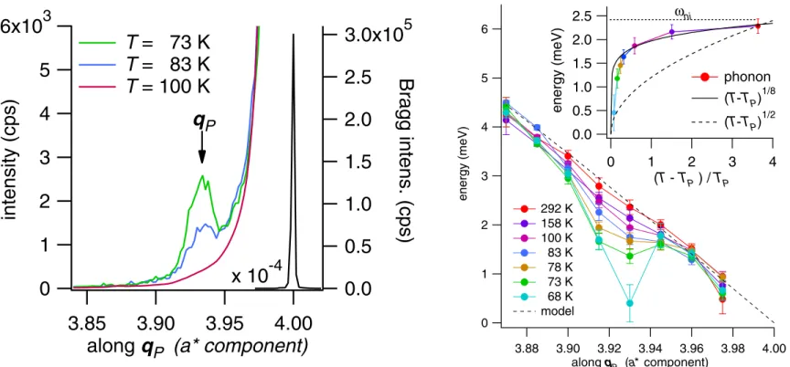
a! 25 A ! and !
c< 10 A ! for o-VIII. Our samples are highly uniform, strongly indicating that the CDW occupies the entire sample volume and not a fraction.
Samples were mounted in a closed-cycle cryostat on a four-circle diffractometer on beam line BW5 at the DORIS storage ring (DESY). This allowed access to a wide range of reciprocal space (h, k, ‘) expressed in units of (2"=a, 2"=b, 2"=c) at temperatures down to 6 K.
A CDW modulation with characteristic wave vector q
CDWgives rise to satellites around reciprocal lattice points at positions Q ¼ ! # q
CDW. High energy x-ray diffraction is sensitive to the atomic displacements parallel to the scattering vector Q [2]. Our previous measurements [2]
on o-VIII showed q
CDW¼ ð #
1; 0; 0:5 Þ and (0, #
2, 0.5) (see Table I). Figures 1(a) and 1(b) show k scans performed on YBCO o-II through the positions (0, #, ‘) and (0, 2 & #, ‘), with ‘ ¼ 0:5 and 6.5 and # ! 0:3. No CDW peaks were found at ‘ ¼ 0:5, but well-defined peaks were observed at
‘ ¼ 6:5. These peaks constitute the first direct x-ray evi- dence for CDW order in YBCO o-II and indicate that the displacements are mainly polarised along c. For compari- son, k scans through the positions (0, 2 & #, ‘) in o-VIII
and o-III are shown in Figs. 1(c) and 1(d) for ‘ ¼ 0:5 and 6.5; again, for modulations along k, the signal at
‘ ¼ 6:5 is stronger.
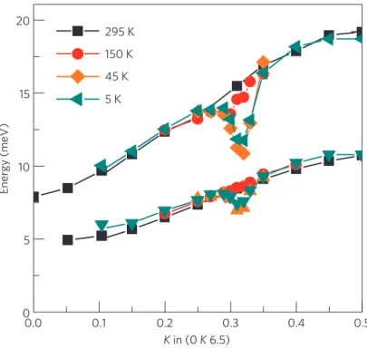
In YBCO o-VIII and III, a lattice modulation is found along both the a- and b-axis directions [1–3]. For o-II, we have searched for a CDW along the a axis, concentrating on positions where a signal was observed in o-VIII. Wave vectors ( j n & # j , 0, ‘) with n ¼ 2, 4 for ‘ ¼ 0:5 and n ¼ 0, 2, 4 for ‘ ¼ 6:5 were measured, and no signal from a lattice modulation was found above the noise level [see Figs. 2(a) and 2(b)]. However, see also the Note added in proof at the end.
Even though the CDW structures in YBCO o-II, III, and VIII are different, the signals from the b-axis modulation have a very similar dependence on ‘, T , and the magnetic field. Figure 3(a) shows the ‘ dependence near ‘ ¼ 6:5 at T ! T
c. All three compounds have a broad peak at ‘ ' 6:5, with a width corresponding to a correlation length of !
c&
10 A. The ! T dependence of several reflections is plotted in Fig. 3(c). As was previously shown for YBCO o-VIII and o-III [1–3], the intensity grows below an onset temperature T
CDW( ! 140 K) down to the respective T
c’s, below which a partial suppression takes place. Here, we show a similar behavior in o-II but with a slightly higher onset tempera- ture. The application of a magnetic field enhances the low-T intensity in a similar fashion to that reported in YBCO o-VIII [2]. It is interesting to note [see Fig. 3(b)]
that the width of the Bragg peak becomes smaller in a field with 11.5 T along c, corresponding to an increase of correlation length !
bfrom 48 # 9 to 63 # 7 A. The ! presence of a magnetic field suppresses superconductiv- ity, and the resurgent competing CDW increases its correlation length.
Modeling of our b-direction data for all three dopings suggests that the displacement pattern involves c-axis
(a) (b) (c) (d)
FIG. 1 (color online). k scans through the CDW wave vector positions (0, #
2, ‘) and (0, 2 & #
2, ‘) in YBCO o-II, VIII, and III at T ! T
c. (a),(b) For o-II, #
2¼ 0:328 ð 2 Þ incommensurate peaks are only observed at ‘ ¼ 6:5, suggesting a strong CDW displacement along z. (c),(d) For o-VIII and o-III, peaks are observed at ‘ ¼ 0:5 and 6.5 with #
2¼ 0:314 ð 2 Þ and 0.308(2), respectively. Linear backgrounds have been subtracted in (a) and (b). To avoid contamination from weakly T-dependent spurious peaks in (c) and the o-III superlattice peak from the minority domain in (d), we plot I ð T
cÞ & I ð 140 K Þ , corrected for a sloping background, as in (a) and (b).
Intensities in (a) and (b) have been multiplied by a factor of 3 to compensate for the smaller o-II sample size.
TABLE I. Characteristics of the YBa
2Cu
3O
ysamples studied.
The superconducting T
cwas determined from the 1 Oe field- cooled magnetization, and doping was evaluated from Ref. [19].
T
CDW, #
1, and #
2are derived from our high energy x-ray experiments—see also the note added at the end of this Letter—(quoted uncertainties in the values of # are dominated by minor crystal alignment errors) and from Ref. [3].
y in Oxygen Doping T
cT
CDW#
1ð a Þ #
2(b) YBCO ordering level p (K) (K) (r.l.u.) (r.l.u.) 6.54 o-II 0.104 58 155(10) 0.320(2) 0.328(2) 6.67 o-VIII 0.123 67 140(10) 0.305(2) 0.314(2) 6.75 o-III 0.132 74 140(10) 0.30 [3] 0.308(2)
PRL 110, 137004 (2013) P H Y S I C A L R E V I E W L E T T E R S week ending 29 MARCH 2013
137004-2
X-Ray Diffraction Observations of a Charge-Density-Wave Order in Superconducting Ortho-II YBa
2Cu
3O
6:54Single Crystals in Zero Magnetic Field
E. Blackburn,
1J. Chang,
2,3,*M. Hu¨cker,
4A. T. Holmes,
1N. B. Christensen,
5Ruixing Liang,
6,7D. A. Bonn,
6,7W. N. Hardy,
6,7U. Ru¨tt,
8O. Gutowski,
8M. v. Zimmermann,
8E. M. Forgan,
1and S. M. Hayden
91School of Physics and Astronomy, University of Birmingham, Birmingham B15 2TT, United Kingdom
2Institut de la matie`re complexe, Ecole Polytechnique Fe´derale de Lausanne (EPFL), CH-1015 Lausanne, Switzerland
3Swiss Light Source, Paul Scherrer Institut, CH-5232 Villigen PSI, Switzerland
4Condensed Matter Physics & Materials Science Department, Brookhaven National Laboratory, Upton, New York 11973, USA
5Department of Physics, Technical University of Denmark, DK-2800 Kongens Lyngby, Denmark
6Department of Physics & Astronomy, University of British Columbia, Vancouver, Canada V6T 1Z1
7Canadian Institute for Advanced Research, Toronto, Canada M5G 1Z8
8Deutsches Elektronen-Synchrotron DESY, 22603 Hamburg, Germany
9H. H. Wills Physics Laboratory, University of Bristol, Bristol BS8 1TL, United Kingdom (Received 16 December 2012; published 28 March 2013)
X-ray diffraction measurements show that the high-temperature superconductorYBa2Cu3O6:54, with ortho-II oxygen order, has charge-density-wave order in the absence of an applied magnetic field. The dominant wave vector of the charge density wave is qCDW ¼ð0;0:328ð2Þ;0:5Þ, with the in-plane component parallel to thebaxis (chain direction). It has a similar incommensurability to that observed in ortho-VIII and ortho-III samples, which have different dopings and oxygen orderings. Our results for ortho-II contrast with recent high-field NMR measurements, which suggest a commensurate wave vector along thea axis. We discuss the relationship between spin and charge correlations inYBa2Cu3Oy and recent high-field quantum oscillation, NMR, and ultrasound experiments.
DOI:10.1103/PhysRevLett.110.137004 PACS numbers: 74.72.$h, 61.05.cp, 71.45.Lr, 74.25.Jb
Charge density waves (CDWs) have recently been observed in the high-temperature superconductors (HTSs)
YBa2Cu3Oy(YBCO) and
ðY;NdÞBa2Cu3Oy[1–3]. The CDW, which competes with HTSs, develops in a region inside the celebrated pseudogap phase, where a number of other probes, including high-field NMR [4], the Kerr effect [5], and the Hall effect [6], show signatures of electronic ordering. This last effect is smoothly connected to the low- temperature high-field quantum oscillations (QOs) [7] that demonstrated the existence of small Fermi surface pockets.
The existence of ground states with competing order is central to many theories of HTSs. A widely discussed example is ‘‘stripe order,’’ that is, a state with coexisting charge and spin order [8]. Stripe order is observed in some HTSs and related compounds, such as
La2$xBaxCuO4[9]
and
La1:6$xNd0:4SrxCuO4[10]. It is important to establish whether the tendency toward stripes is a generic property of the cuprates and whether the spin and charge correla- tions are always related.
YBa2Cu3Oy
differs from, e.g.,
La2$xðBa;SrÞxCuO4, in that it contains bilayers of
CuO2planes, separated by layers containing a certain fraction (depending on
y) ofCu-O chains. The oxygen-filled chains, which run along the orthorhombic crystal
bdirection, tend to order and are labeled ortho-N, depending on the repeat length (Na) of the ordering of the chains along
a[11–13]. A major gap in the CDW picture to date was the failure to observe a CDW in the ortho-II state (the most highly ordered state,
having alternatingly full and empty Cu-O chains). This was surprising because many studies of this composition had suggested that such an order is present, at least in a high field [4,6,14–17]. Most recently, ultrasound measurements have indicated a two-q state in high magnetic fields [18].
In this Letter, we report the observation of a CDW in an ortho-II sample of
YBa2Cu3O6:54in a zero magnetic field with dominant wave vector
qCDW¼ð0;0:328ð2Þ;0:5Þ. This contrasts with both lower and higher dopings, where two wave vectors are observed corresponding to two mod- ulations of similar amplitude [1–3]. Both the wave vector magnitude and the direction of
qCDWdiffer from those inferred from NMR measurements in a high field [4].
The propagation vectors of the charge and spin correlations in ortho-II YBCO do not appear to follow the simple relationship
!charge ¼2!spinobserved in stripe systems [9,10]. We examine the doping dependence of the CDW order in high quality ortho-II, III, and VIII samples (hereafter denoted as o-II, o-III, and o-VIII).
We carried out high energy (100 keV) x-ray diffraction experiments on three
%99%detwinned
YBa2Cu3Oysingle crystals (sample characteristics are given in Table
I). Thesesamples have orthorhombic crystal structures [a
&3:82(ignoring the chain-ordering superlattices),
b&3:87, and c&11:7 A]. The o-II sample shows a more perfect!oxygen-chain order than the other compositions. The coherence lengths are
!a%110A;! !b>150A!and
!c¼ 55A!for o-II,
!a%20A!and
!c<10A!for o-III, and PRL
110,137004 (2013) P H Y S I C A L R E V I E W L E T T E R S
week ending29 MARCH 2013
0031-9007= 13=110(13)=137004(5) 137004-1
!2013 American Physical Society
we start from the far-right side ofFigure 1, in the overdoped metallic state. This state is characterized by a large Fermi surface that has a volume containing 1 þ p holes per Cu atom, as determined by angle-dependent magneto-resistance (11), angle-resolved pho- toemission spectroscopy (12), and quantum oscillations (13), all performed on the single- layer cuprate Tl2Ba2CuO6þd (Tl-2201). The low-temperature Hall coefficient RH of overdoped Tl-2201 is positive and equal to 1 /e(1þp) (14), as expected for a single-band metal with a hole densityn¼1þp. Conduction in the normal state obeys the Wiedemann- Franz law (15), a hallmark of Fermi-liquid theory. At the highest doping, beyond the superconducting phase (Figure 1), the electrical resistivity r(T) of Tl-2201 exhibits the standardT2temperature dependence of a Fermi liquid (16), also observed in La2–xSrxCuO4
(LSCO) (17).
3. SCATTERING AND PAIRING
The question then is this: What makes superconductivity emerge from this particular, rather conventional, metal? The critical doping at which superconductivity springs is roughly the same in all hole-doped cuprates, namely pc # 0.27. Note that although it appears to obey weak-coupling BCS theory, at least initially (15, 18), the superconducting state has d-wave symmetry (19) rather than the usual s-wave symmetry, pointing to an electronic rather than phononic pairing mechanism (20). What happens at pc to make d-wave pairing prevail? Let us investigate one intriguing clue: At this special doping, the scattering between electrons undergoes a qualitative change. Indeed, it is precisely belowpc
0
Pseudogap phase
pc Metal
AF insulator
p*
TN T*
Tc
Hole concentration, p
Temperature, T (K)
ps
0.0 0.1 0.2 0.3
200
100
Superconductor
Figure 1
Schematic phase diagram of cuprate superconductors as a function of hole dopingp. The Mott insulator at p¼0 shows antiferromagnetic (AF) order belowTN, which vanishes rapidly with doping. At high doping, the metallic state shows all the signs of a conventional Fermi liquid. At the critical dopingpc, two events happen simultaneously: Superconductivity appears (below a critical temperatureTc), and the resistivity deviates from its Fermi-liquid behavior, acquiring a linear temperature dependence. The simultaneous onset ofTcand linear resistivity is the starting point for our exploration of cuprates. The evolution from metal to insulator is interrupted by the onset of the pseudogap phase that sets in below a crossover temperatureT$, which goes to zero at a quantum critical point (QCP) located atp$ in the absence of superconductivity (removed, for example, by application of a large magnetic field). The existence, nature, and location of such a QCP are a major focus of this review. In the presence of superconductivity, the QCP may move to lower doping, down topS, as a result of a competition between the pseudogap and superconducting phases (9, 10).
Fermi surface: boundary ink-space that separates occupied electron states from unoccupied states; its volume is directly proportional to the carrier density; when closed, it can be electron-like (enclosing occupied states) or hole-like (enclosing unoccupied states) Quantum oscillations:
oscillations in the resis- tance or magnetization of a metal as a function of magnetic fieldBthat results from cyclotron motion and Landau quantization of energy levels; their frequency in 1/Bis proportional to the cross-sectional area of a closed Fermi surface
www.annualreviews.org % Scattering and Pairing in Cuprate Superconductors 53 Annu. Rev. Condens. Matter Phys. 2010.1:51-70. Downloaded from www.annualreviews.org Access provided by University of Zurich - Hauptbibliothek on 09/24/18. For personal use only.
Charge Ordering in
YBa 2 Cu 3 O 7-x
- Kohn Anomaly: Spectroscopy
- New lattice modulation: X-ray diffraction
How to observe – charge ordering
- Charge modulation: STM
- Fermi Surface Reconstruction: Hall effect
- Fermi Surface Reconstruction: ARPES
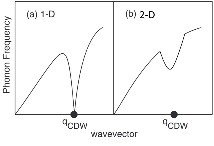
dictated by the ~ q-dependent electron – phonon coupling (EPC) (4 – 7). Mazin and coworkers used the classical CDW materials NbSe 2 , TaSe 2 , and CeTe 3 to justify their conclusion and showed that with a proper inclusion of EPC the observed properties could be explained (4, 6, 7). It is then obvious that experimentally we should be exploring the phonon spectra in detail to determine the
~ q dependence of EPC (8). One may argue that both FSN and EPC are forms of electron – lattice interaction, involving excitations of electrons from filled to empty states. However, they should be distinguished because FSN involves elastic scattering, whereas EPC involves inelastic scattering from the lattice.
Although it is possible that when the dimensionality is truly re- duced, the CDW state will be tied intimately to FSN, it is appro- priate at this stage to quote Peierls (ref. 9, p. 29): “ This (Peierls) instability came to me as a complete surprise when I was tidying material for my book (1955), and it took me a considerable time to convince myself that the argument was sound. It seemed of only academic significance, however, since there are no strictly one-di- mensional systems in nature. I therefore did not think it worth publishing the argument, beyond a brief remark in the book, which did not even mention the logarithmic behavior. ” A recent theo- retical work indicated that Peierls ’ intuition might have been cor- rect (4). Density functional theory calculations were performed for a 1D chain of Na atoms, which should be the best representation of a perfect Peierls system. With the atoms clamped there was no sign of an electronic-only density wave, and relaxation of the ion po- sition in the 1D chain failed to produce any distortion, i.e., no Peierls distortion. However, if the ions were allowed to move in 2D, the lowest energy state was a zigzag chain, but the electronic gap anticipated in the Peierls CDW phase was missing (4).
Experimentally a whole host of techniques must be used to fully characterize the properties associated with a CDW. Angle- resolved photoemission spectroscopy (ARPES) can determine the band structure and the Fermi contour (10 – 12) that are needed to calculate the electronic susceptibility. Electron (13, 14), X-ray (15), and neutron diffraction (16, 17) measurements
can determine the structure, ~ q CDW , and T CDW . Scanning tun- neling microscopy (STM) and spectroscopy (18, 19) can de- termine the wave length of the charge modulation as well as the electronic transition temperature. Inelastic neutron (16, 17) and X-ray scattering (20) can probe the temperature dependence of the Kohn anomaly in the phonon dispersion. Transport mea- surements (21) can reveal the transition temperature and the metal insulator transition predicted by the Peierls model. Finally, because EPC is important, high-resolution ARPES data are needed to estimate the strength of the EPC in a CDW system (22).
Here we stress the importance of the phonon dispersion and linewidth measurements are to understand the origin of CDWs.
To illustrate the importance of EPC in the formation of a CDW state we briefly describe the classic and the most studied CDW system, NbSe 2 (23), a layered quasi-2D material. This material has a hexagonal layered structure with lattice con- stant of 3.443 Å. A CDW phase transition occurs with q CDW ≅ ð 2=3 ÞjΓ M j = 0:695 Å − 1 [ Γ and M are the points at the center and boundary in the Brillouin zone (BZ), respectively, in the high-temperature phase] at T CDW = 33.5 K (15, 17) (shown in Fig.
2A). All of the data and the modeling for this system dramatically
A
k F
-k F 0 k
1D: Peierls B
C 2D: Fermi Surface
k x
k y
Fermi Surface
q k F
k F
k F k F
q D
1D: Kohn Anomaly
0
2D 1D
3D 1D
Lindhard Function
Fig. 1. Schematic representations of the physical phenomena associated with Fermi surface nesting. (A) The plot of the one-dimensional free electron band structure for a chain of atoms with separation a and one electron per atom site. The location of the Fermi energy is indicated with the nesting vector q. (B) Kohn anomaly in the acoustic phonon branch as a function of temperature, which results from Fermi surface nesting. (C ) The Fermi con- tour of a 2D free electron system. (D) Lindhard response function χ 0 ð ~ q Þ as a function of dimensionality (1). The dotted line shows the effect of 2%
deviation from perfect FSN and Inset shows a small Drude relaxation (4).
A B
C
D E
F G
Ts
q q
( )
1( )
Fig. 2. Properties of the CDW in NbSe 2 . (A) Fermi surface contours (10) with the experimental ~ q CDW (16, 17) shown. (B and C ) Re χ 0 ð q Þ and Im χ 0 ð q Þ cal- culated from experimental data (10) along the Γ – M direction. (D) STM image of the CDW phase at T = 22 K. Inset shows the fast Fourier transform (19). (E ) STM image at a temperatures above T CDW (19). (F ) Order parameter of the lattice transition associated with the CDW (17). (G) Resistivity as a function of temperature, with the superconducting and CDW transition temperatures indicated (21). D and E are modified with permission from ref. 19, copyright the American Physical Society.
2368 | www.pnas.org/cgi/doi/10.1073/pnas.1424791112 Zhu et al.
Kohn Anomaly – 1D
Classification of charge density waves based on their nature
Xuetao Zhu a,1 , Yanwei Cao a,1 , Jiandi Zhang b , E. W. Plummer b,2 , and Jiandong Guo a,2
a
Beijing National Laboratory for Condensed-Matter Physics and Institute of Physics, Chinese Academy of Sciences, Beijing 100190, China; and
bDepartment of Physics and Astronomy, Louisiana State University, Baton Rouge, LA 70808
Contributed by E. W. Plummer, January 7, 2015 (sent for review August 15, 2014; reviewed by Takeshi Egami and Steven G. Louie)
The concept of a charge density wave (CDW) permeates much of condensed matter physics and chemistry. CDWs have their origin rooted in the instability of a one-dimensional system described by Peierls. The extension of this concept to reduced dimensional systems has led to the concept of Fermi surface nesting (FSN), which dictates the wave vector ( ~ q CDW ) of the CDW and the corre- sponding lattice distortion. The idea is that segments of the Fermi contours are connected by ~ q CDW , resulting in the effective screen- ing of phonons inducing Kohn anomalies in their dispersion at
~ q CDW , driving a lattice restructuring at low temperatures. There is growing theoretical and experimental evidence that this picture fails in many real systems and in fact it is the momentum depen- dence of the electron – phonon coupling (EPC) matrix element that determines the characteristic of the CDW phase. Based on the published results for the prototypical CDW system 2H-NbSe 2 , we show how well the ~ q-dependent EPC matrix element, but not the FSN, can describe the origin of the CDW. We further demonstrate a procedure of combing electronic band and phonon measure- ments to extract the EPC matrix element, allowing the electronic states involved in the EPC to be identified. Thus, we show that a large EPC does not necessarily induce the CDW phase, with Bi 2 Sr 2 CaCu 2 O 8+ δ as the example, and the charge-ordered phenom- ena observed in various cuprates are not driven by FSN or EPC. To experimentally resolve the microscopic picture of EPC will lead to a fundamental change in the way we think about, write about, and classify charge density waves.
charge density wave | phonon | nesting
T he phrase charge density wave (CDW) was first used by Fröhlich (1, 2) but originates from Peierls ’ description of a fundamental instability in a one-dimensional (1D) chain of atoms equally spaced by a lattice constant a (2). Fig. 1A shows the free electron band of such a 1D chain with one electron per atomic site. The Fermi points are at k F = ±π /2a and are con- nected by the nesting vector q = 2k F . In 1930 Peierls asserted that this system is unstable, showing an electronic disturbance with the wave vector 2k F , changing the periodicity of the chain, and opening up a gap at the zone boundary (k = π /2a) of the new unit cell containing two atoms (1, 2). The conjecture was that the gain in electronic energy would always overwhelm the cost of restructuring the atoms (1). Consequently in the Peierls model there would be a transition from the metallic high-temperature state to the insulating-dimerized ground state at a critical tem- perature T CDW . Kohn (3) pointed out that there is an image of the Fermi surface in the vibrational spectrum, because the zero energy electronic excitations at 2k F will effectively screen any lattice motion with this wave vector. Fig. 1B shows the phonon dispersion for this 1D chain at different temperatures (1). Below T CDW the phonon energy at q = 2k F becomes imaginary, meaning there is a new lattice structure. Above T CDW there is a sharp dip (Kohn anomaly) in the phonon dispersion but no static restructuring.
The question is how to extend the Peierls picture to real sys- tems in higher dimensions (a real one-dimensional system is only quasi-1D). A standard practice is to calculate the susceptibility
χ ð ~ q; ω Þ for a given electronic configuration (1) and to use the zero energy value of the Lindhard response function χ 0 ð ~ q Þ ≡ χ 0 ð ~ q; ω = 0 Þ (SI Text) to determine whether the electron response can drive a Peierls phase transition ― there should be a peak in the imaginary part of the response function Im ½ χ 0 ð ~ q Þ$ at the Fermi surface nesting (FSN) vector ~ q CDW as well as in the real part Re ½ χ 0 ð ~ q Þ$ , because the real part defines the stability of the system (4). Fig. 1D shows the plot of Re ½ χ 0 ð ~ q Þ$ for a free electron system in 1D, 2D, and 3D (1), respectively, whereas Fig. 1C displays the free-electron Fermi contour in 2D. There is a logarithmic di- vergence in Re ½ χ 0 ð ~ q Þ$ for the 1D system but no peaks in the 2D and 3D electron gases. If CDWs are created by FSN, the Fermi contour must have been distorted to create nesting as represented by Re ½ χ 0 ð ~ q Þ$ . In a seminal paper Johannes and Mazin demon- strated that the logarithmic divergence of Re ½ χ 0 ð ~ q Þ$ is not robust against small deviations from perfect nesting (4). The dotted line in Fig. 1D illustrates what happens for only a 2% deviation in k F from perfect nesting and Fig. 1D, Inset, shows the effect of including a small “ Drude relaxation ” in the calculation for the susceptibility.
If FSN is the origin of the CDW as in the Peierls picture, the real and imaginary parts of the susceptibility calculated using the measured band structure should both show strong peaks at ~ q CDW , there should be a Kohn anomaly in all of the phonons (except ones not allowed by symmetry) at ~ q CDW (4), and at least one of the modes must go imaginary at low temperature, inducing a lattice distortion and an electronic gap. However, Johannes and Mazin argued, “ only a tiny fraction if any, of the observed charge ordering phase transition are true analogs of the Peierls instability . . . ” (ref. 4, p. 1). In fact, it has been postulated that CDW phases are
Significance
Charge density waves (CDWs) are observed in many solids, especially in low-dimensional systems. Their existence was first predicted in the 1930s by Rudolf Peierls, who prophesied that CDWs would exist in an ideal one-dimensional (1D) chain of atoms, lowering the energy of the system and driving a re- construction of the lattice. In 1959, Walter Kohn pointed out that this nesting results in what is now known as a “ Kohn anomaly, ” a simultaneous softening of coherent lattice vibra- tions, i.e., phonon softening. This simple textbook picture of the origin of CDWs does not seem to be correct in many materials and in this report we propose a previously un- identified classification of CDWs based upon their nature.
Author contributions: X.Z., Y.C., J.Z., E.W.P., and J.G. designed research; X.Z., Y.C., and J.G.
performed research; X.Z., Y.C., J.Z., E.W.P., and J.G. analyzed data; and X.Z., J.Z., E.W.P., and J.G. wrote the paper.
Reviewers: T.E., University of Tennessee; and S.G.L., University of California, Berkeley.
The authors declare no conflict of interest.
Freely available online through the PNAS open access option.
1
X.Z. and Y.C. contributed equally to this work.
2