semiconductors in complex
environments and under external fields
DISSERTATION ZUR ERLANGUNG DES DOKTORGRADES DER NATURWISSENSCHAFTEN (DR. RER. NAT.)
DER FAKULT ¨ AT F ¨ UR PHYSIK DER UNIVERSIT ¨ AT REGENSBURG
vorgelegt von
Jonas Zipfel
aus Regensburg
Februar 2020
Pr¨ufungsausschuss: Vorsitzender: Prof. Dr. Vladimir Braun Erstgutachter: Dr. Alexey Chernikov Zweitgutachter: Prof. Dr. Christian Sch¨uller weitere Pr¨ufer: Prof. Dr. Dominique Bougeard
semiconductors in complex
environments and under external fields
DISSERTATION ZUR ERLANGUNG DES DOKTORGRADES DER NATURWISSENSCHAFTEN (DR. RER. NAT.)
DER FAKULT ¨ AT F ¨ UR PHYSIK DER UNIVERSIT ¨ AT REGENSBURG
vorgelegt von
Jonas Zipfel
aus Regensburg
Februar 2020
1 Introduction
52 Theoretical background
92.1 Basic properties of transition metal dichalcogenides
. . . 92.1.1 Crystal structure . . . 10
2.1.2 Electronic structure . . . 12
2.1.3 Electro-optical properties - Excitons . . . 15
2.2 Excitons in high magnetic fields
. . . 252.2.1 Valley Zeeman effect . . . 25
2.2.2 Diamagnetic shift . . . 27
2.2.3 Landau level splitting . . . 28
2.3 Environmental sensitivity of exciton properties
. . . 312.3.1 Effects of dielectric screening on exciton states . . . 31
2.3.2 Dielectric environment as a source of disorder . . . 33
2.4 Exciton Propagation
. . . 352.4.1 Diffusive propagation of excitons . . . 35
2.4.2 Saha equilibrium of charge carriers . . . 38
2.4.3 Coupled exciton-plasma diffusion . . . 40
2.5 Organic-inorganic 2-dimensional semiconductors: Perovskites
42 2.5.1 Structure of layered halide perovskites . . . 422.5.2 Electronic structure . . . 44
2.5.3 Electro-optical properties . . . 45
3 Experimental methods
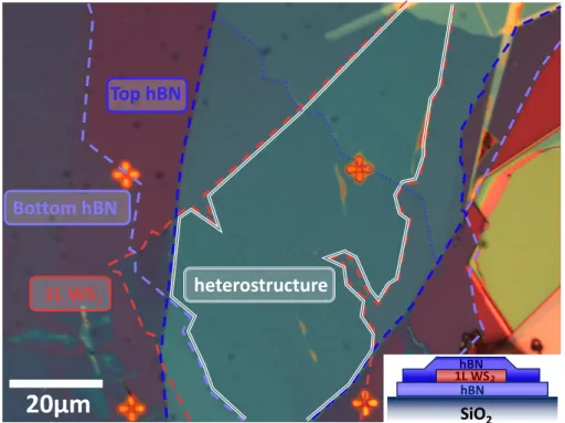
473.1 Sample preparation
. . . 473.1.1 Exfoliation of monolayer TMDCs . . . 47
3.1.2 Fabrication of TMDC heterostructures . . . 49
3.1.3 Preparation of encapsulated perovskite samples . . . 50
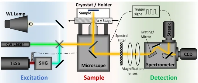
3.2 Experimental setup
. . . 523.2.1 General spectroscopy setup . . . 52
3.2.2 High magnetic field setup . . . 53
3.3.1 Analyzing reflectance spectra - a transfer matrix approach . . . 56
3.3.2 Diffusion coefficients from time resolved photoluminescense . . . 60
4 Results and discussions
634.1 Excitons in high magnetic fields
. . . 634.1.1 Measurements in high magnetic fields . . . 64
4.1.2 Magnetic field dependent exciton resonance shifts . . . 65
4.1.3 Quantitative valley Zeeman and diamagnetic shift . . . 67
4.1.4 Exciton radii from diamagnetic shifts . . . 69
4.2 Influence of the environment in experiments
. . . 734.2.1 Resonance broadening from nanoscale disorder . . . 73
4.2.2 Suppression of nanoscale disorder . . . 77
4.2.3 Probing disorder fluctuations on the microscale . . . 79
4.2.4 Conventional sources of disorder . . . 82
4.3 Exciton transport in disorder-free structures
. . . 864.3.1 Exciton propagation dynamics under ambient conditions . . . . 86
4.3.1.1 Predicted exciton diffusion in disorder-free structures . 90 4.3.1.2 The Saha equilibrium under experimental conditions . 93 4.3.1.3 Experimental compound exciton-plasma diffusion . . . 94
4.3.1.4 Influence of doping on the Saha equilibrium . . . 96
4.3.2 Exciton propagation at low temperatures . . . 98
4.3.2.1 WSe2 photoluminescence at low temperatures . . . 99
4.3.2.2 Phonon-assisted emission from dark exciton states . . 102
4.3.2.3 Neutral exciton propagation at low temperatures . . . 106
4.4 Exciton transport in 2D perovskite systems
. . . 1114.4.1 Stability of perovskites . . . 111
4.4.2 Exciton dynamics in monolayer perovskites . . . 114
4.4.3 Exciton propagation in monolayer perovskites . . . 115
5 Summary and outlook
119Acknowledgements
123Bibliography
125Introduction
Preface - a few personal considerations
Writing this first part of the work I find myself at a point where it is commonly expected to give a motivation for what has been researched. This immediately leads me to confront the question, that I have heard what feels like a thousand times over the course of this work: ”What can it be used for?”. In terms of the audience reached with this work, such a question might have less relevance, however, given how often I encountered it, also in scientific surroundings, it at least deserves a few words of consideration. Quite obviously it can be extended to a bigger philosophical magnitude of questioning what anything is ever useful for, that has racked many a brains and is far beyond the few words I will spare it here. Yet I feel the need to give at least a somewhat satisfactory justification for why I have put three years of work into this research. Turning back to the question under the aspect of whether this work has direct relevance for any applications, I can honestly state that I do not know. But I also do not think that it is the relevant question here. Research can and should not be judged on whether it yields direct relevance or use for novel applications. It is rather directed in gathering information about promising systems, concepts or ideas, with no certainty of whether the proposed big breakthrough is found in the end. In a way it is comparable to the prominent parabola of exploring a cave, where someone might choose a certain branch-off, not knowing whether he finds a dead end or the anticipated light at the end of the tunnel. In this context it is common to encounter one or the other dead end, or find no exit at all, but that should not stop us from searching. The gathered information can be used to draw a map of a bigger picture, that is then of assistance for further (re)searches. The more important question is thus, whether choosing a certain path can yield new, relevant or helpful information based on what we already know. With that being put up front, let me try to give the expected motivation, in terms of simply introducing the branch of the tunnel that we are in, for this particular work. It is then upon the individual reader to assess, whether, in the context of existing technologies, concepts and ideas, it is worth to be further pursued.
Motivation
Understanding, controlling and manipulating charge carriers has been the fundamental concept of everyday information technology, since at least the demonstration of the first working transistor in 1948 [1] and thus lays the very foundation for almost every electrical or opto-electrical device based on semiconducting materials. An ever increas- ing demand of computing power, while at the same time keeping devices of handy size, has long called to the need for a shrinking of the individual operating units [2]. How- ever, the miniaturization of electronic devices has also manifested itself particularly in making devices thinner, with futuristic concepts such as fully transparent and flexible devices starting to take a hold in everyday life [3–5]. From a more realistic point of view this rises the quite general and omnipresent question of ”where are the limits?”.
Given the state of the art understanding of solid state physics, the answer to such a question is readily found in the smallest stable material quantity known to us: a single atom. Now while it is widely known that atoms do not live up to the greek etymology of their name-giving as being ’indivisible’, a single layer of atoms does still constitute the thinnest stable material system one can imagine to exist.
On one hand, just taking the concept of such a system, it is found that the reduc- tion of a material’s dimensions to such dramatic extent brings along intriguing aspects to consider. It is well understood, that such dimensional confinement leads to arising quantization effects in their electronic structure [6], resulting in a wide range of novel physical concepts and properties, readily utilized in state of the art opto-electrical tech- nologies [7]. However, the room for postulated ideas and potential applications in this world of quantum-engineering is still seemingly limitless [8]. On the other hand, one should recognize what results from the fact of a material really being intrinsically two- dimensional in a realistic scenario. Following this thread of thought, it is of particular interest to refer to a famous saying, attributed to Pauli [9], stating that the surfaces of materials were ”made by the devil”. They set a boundary to the well ordered and structured system of the bulk material and thus give rise to a source for significant amounts of inhomogeneities, disorder and impurities [10]. In sufficiently big bulk ma- terials, electronic properties are dominated by the volume and the influence of these surface and interface states is mostly of subordinate importance. However, decreasing the dimensionality of a structure then calls back the significance of precisely such states.
In the limit of single layers of atoms, that are materials of inherent two-dimensional character, this is taken to the extreme, as they can also be viewed to be pure surfaces.
Following Pauli’s reasoning one would then come to the conclusion, that such materials are of the devil’s own making, as reducing their size to such fundamental limits intro- duces a potential for chaotic amounts of disorder. In this context however, it should
of materials thus gives ways to proverbially play tricks on the devil, in the means of making use of exactly that pronounced surface sensibility. It opens up a whole new way of influencing and controlling charge carrier dynamics, that is in form of the material’s directsurroundings. In contrast to conventional quantum well systems, this might even be extended to the concept of combining multiple such single-atom layers via lateral stacking to create novel materials with entirely unseen electronic properties [13].
Resulting from such concepts and ideas follows an incentive for the search of materi- als and structures that approach such a two-dimensional limit, while at the same time holding suitable and intriguing electronic properties. By now there are a wide range of available ultra-thin materials from all different material classes, including metals, semi-metals, semiconductors, insulators, superconductors etc. [14–16] An important class of such materials is found in single layers of van-der-Waals crystals, due to the discovery that monolayers of such materials can be easily fabricated through exfoliation of mono-crystalline bulk crystals. First prominently demonstrated on the example of graphite, yielding single layers of graphene [17, 18], a rapidly evolving field of these two-dimensional crystals was established, with van-der-Waals crystals spanning a huge variety of available and stable elemental compositions [19].
A sub-class of such structures that has spread wide interest in the scientific com- munity over the past several years is that of the two-dimensional semiconductors, in particular in the form of monolayers of transition metal dichalcogenides (TMDC). This is mainly due to two important intrinsic properties. On the one hand, as first demon- strated for the compound of MoS2 [20, 21], TMDCs have direct bandgap character in the monolayer limit. On the other hand, as a result from quantum and dielectric confinement, Coulomb interactions in these systems are significantly enhanced [22,23].
This gives rise to the formation of extraordinarily tightly bound electron-hole pairs, called excitons. These quasi-particles are found to have binding energies sufficiently high (∼500 meV) to make them stable under ambient conditions and therefore domi- nate the charge carrier properties of these materials even under room temperature [24].
Together these two properties lead to remarkably efficient light-matter coupling in these materials. From such intriguing properties follows a variety of proposed concepts, including the fabrication of artificial heterostructures as mentioned above [25], seem- ingly well accessible from simple and efficient fabrication methods, such as exfoliation and subsequent stamping onto desired substrates [26]. While such methods lack scal- ability, they turn out to be a suitable and efficient approach to build even complex structures on a laboratory scale. From that, the easy access to exciton dynamics via optical means made these two-dimensional structures a prototypical platform for the
study of fundamental physical concepts and effects, arising from the quantum confine- ment in one direction. It has turned out to be of particular interest for the investigation of excitonic properties in systems where, in contrast to conventional semiconductors, excited charge carriers are generally not found in an unbound state. Here, a wide range of novel physical phenomena can be studied. In particular, it is of interest to point towards the physical behavior found in connection with excitons in these systems, bar- ing remarkable resemblance to the concept of a hydrogen atom as known from classical atomic physics. Such findings include an excitonic Rydberg series of excited states [27, 28], charged excitons [29, 30] or even exciton aggregates, so called biexcitons [31–33].
Additionally their peculiar band structure gives rise to riveting effects, such as coupling of spin and valley degree of freedom, allowing for the selective optical addressing of spin states and introducing a novel stage for the research of spin phenomena [34–36].
Finally such intriguing exciton properties also give rise to more futuristic opto-electrical innovations and conceptional devices [15, 37, 38], not least arising from the materials’
capability to efficiently transport photoexcitations in the form of correlated electron- hole pairs over considerably large distances [39, 40].
In the frame of this work we use these remarkable electro-optical properties and ded- icate ourselves to the study of fundamental exciton properties. With remark to Pauli’s statement, we show that the material’s optical response can be used to investigate in- fluences of the surroundings, in particular disorder, on the bound charge carrier states, given the two-dimensional character of the structures. Via optical spectroscopy, insight into the exciton ground and excited states’ spatial extent from field induced resonance shifts is given. We further investigate the impact of environmental disorder and more- over study how it can be suppressed in a controlled way, using the concept of above mentioned artificial heterostructures. We then utilize such structures to study exciton transport dynamics and examine the influence of disorder effects by comparing the re- sults to that of pristine monolayers subjected to significant disorder [40].
Finally, we also investigate a different two-dimensional semiconductor system, that of layered halide perovskites. These systems find wide interest, in particular in the use as suitable materials for photo-voltaic devices and their research in the past was indeed driven from a more application oriented point of view. However, their similar optical response compared to TMDC monolayers, in particular the formation of equally tightly bound excitons, has sprung an incentive for are more in-depth understanding of their general electro-optical properties. We show that our theoretical understanding, as well as experimental methods from the study of two-dimensional TMCD structures can be extended to such systems. Moreover, we find that it provides a way to empirically study fundamental material properties and exciton dynamics that are yet theoretically hard to capture.
Theoretical background
In the first segment of this scientific discourse the necessary theoretical background for the underlying work shall be presented. The first section gives an introduction into the basic properties found in the two-dimensional semiconductor materials of mono- layer transition metal dichalcogenides. Their intriguing electro-optical properties are highlighted with particular focus on the extraordinarily strong light-matter interaction and formation of tightly bound excitons. Hereafter, sections 2.2-2.5 are dedicated to more specific topics and the content as well as the structuring follow closely along with experimental results presented inchapter 4, defining a central theme to follow. For this purpose the second section discusses the origin of magnetic field induced energy shifts of exciton resonances and details how these are linked to fundamental properties of the same. The following section outlines the relevance of a material’s surroundings, given an inherent two-dimensional character and how this can affect experimental observations.
In the third section, the concept of excitons as freely moving quasi-particles is detailed and the theoretical description of such transport processes is captured. Finally, in the last section a different two-dimensional semiconductor material class, that of layered hybrid halide perovskites, will be discussed and similarities to the monolayer TMDCs will be illustrated on an empirical basis.
2.1 Basic properties of transition metal dichalco- genides
In this first part we focus on the fundamental properties of transition metal dichalco- genides (TMDC) in the limit of an atomically thin monolayer of the material. While at first a brief introduction to their crystal structure is given, the main focus lies on their electronic structure and resulting electro-optical properties. Particular focus is put on the strong light-matter interaction, dominated by the formation of bound electron-hole pairs (excitons), as a result from quantum and dielectric confinement effects due to their two-dimensional character. While in this context general properties of excitons and exciton formation dynamics in ultra-thin semiconductors are discussed, also more specific concepts, resulting from the unique band structure of TMDC materials, are introduced.
2.1.1 Crystal structure
Real space lattice
Transition metal dichalcogenides (TMDCs) in bulk form are so called van-der-Waals crystals, meaning, that in analogy to the well known graphite, these crystals are built from stacked layers, weakly bound by van-der-Waals forces in the out-of-plane direction.
In the in-plane direction, however, the single layers are formed by strong covalent bonds, resulting in a honeycomb-like hexagonal lattice [41–43]. In contrast to graphite, TMDC layers have two different atoms in their base lattice, shown infig. 2.1(a) in a top view, which leads to a reduced D6h point group symmetry with in-plane lattice constants between two atoms of the same type typically ranging around 3.1-3.3 ˚A [44]. There are three known different stacking orders called 1T, 2H and 3R phases [45], where the 1T phase is a non-stable phase, that is not found to exist naturally [46–48].
K- K+
K- (c)
K+
𝛬- 𝛤
K+
M
K-
𝛬+
2H
(a) (b) (d)
Figure 2.1: Adapted from [45]: (a) Top view of a single layer of a transition metal dichalcogenide crystal, with transition metal atoms in blue and chalcogenides in orange.
The yellow diamond represents the unit cell. (b) Three dimensional cutout of the single layer along the blue triangle shown in (a). (c) First Brillouin zone of a TMDC monolayer including high symmetry points. (d) Schematic representation of the 2H phase, with alternating layers being rotated by 180° and ABAB stacked.
While in principle both 2H and 3R phase can be stable, first principle calculations show the 2H form to be the energetically favorable phase [49]. Accordingly, most of the available TMDC materials are found in the 2H form [50], where alternating layers are stacked in an ABAB pattern on top of each other, with an additional 180° twist angle between adjacent layers (seefig. 2.1(d)). As a consequence only this phase will be considered in the scope of this work. Fig. 2.1(b) shows a cutout of a single layer along
the blue triangle. It can be seen, that a single layer of these materials is made up by basically sandwiching a layer of transition metals between two layers of chalcogenides.
Considering the unit cell of such a crystal illustrated infig. 2.1(a) by a yellow diamond, one yields the stochiometric formula of MX2, where M is a transition metal and X a chalcogen atom. While there are different combinations of elements to form TMDCs, the relevant material systems for this work include only the prominent combinations of M=Mo/W and X=S/Se. From now on referring to TMDCs will only include these four combinations.
Since single layers of such crystals are only weakly bound to one another, it was found that they can be easily separated by mechanical exfoliation down to a single monolayer [17,18]. While this does have immediate consequences for the electronic band structure due to quantum confinement effects (further discussed in the next section), it also leads to breaking of the inversion symmetry [51,52]. A bulk hexagonal lattice in 2H stacking does always have an inversion center in the approximation of the bulk being infinitely big compared to the surface. This approximation, however, breaks down when considering crystals of only few layers. In this limit even numbered layers will still have an inversion center, since in 2H stacking, a transition metal atom of the subsequent layer will always be stacked on top of a chalcogen atom of the previous layer (see fig. 2.1(d)). For odd numbered layers in the few layer limit though, this will lead to a breaking of the inversion symmetry, most easily evident in the case of a monolayer. As a consequence, the symmetry group is reduced to a three-fold rotational symmetry with the point group D3h [45].
Reciprocal lattice
The hexagonal real space lattice of monolayer TMDCs results in the first Brillouin zone of the reciprocal lattice also being hexagonal, as shown in fig. 2.1(c). The blue lining indicates a trace, typically used in band structure calculations, including important high symmetry points such as the K−points at the corners of the first Brillouin zone and the Λ−points (also referred to as Q−points in a bulk crystal), located between Γ−and K−points. Due to the inversion symmetry breaking in the monolayer limit, time reversal symmetry constitutes that high symmetry points are no longer completely equivalent.
Instead, opposing points in the Brillouin zone are distinguishable by different valley indicesτ =±1, meaning only every second point is fully equivalent with the other. This is commonly distinguished by two equivalent notations, either by marking points with + or - (e.g. K+/K-), or marking one of the points with an apostrophe (e.g. K/K’). The result is a similar three-fold rotational symmetry in k-space as in real space, with the Γ−point being the rotation center, which has immediate implications for the resulting electronic structure, discussed in the following [20].
2.1.2 Electronic structure
Transition to a direct semiconductor in the monolayer limit
On the basis of such well defined real space and reciprocal lattices, the resulting elec- tronic band structure shall be presented. Here TMDCs in bulk form are well known to be momentum-forbidden indirect semiconductors [41–44]. However, as mentioned in the previous section, the confinement of TMDCs in one dimension, meaning the transi- tion from bulk to a two-dimensional monolayer material, has direct consequences for its electronic properties. It has been found that this confinement leads to a transition of the monolayer TMDCs’ band structure from an indirect bandgap to a direct bandgap one [20, 21, 53]. This will be showcased in detail on the prominent example of MoS2, although being analogous for the other TMDCs.
In a bulk crystal of the material the bandgap is found between valence band maximum located at the Γ−point and conduction band minimum at the Q−points, as depicted for a calculated band structure of MoS2 in the left panel of fig. 2.2. For a decrease in
Bulk MoS2 4-Layer 2-Layer 1-Layer
𝛤 M K 𝛬 𝛤 𝛤 M K Q 𝛤
𝛤 M K Q 𝛤 𝛤 M K Q 𝛤
Figure 2.2: Adapted from [21]. Calculated change of the MoS2 band structure when transitioning from bulk to the monolayer limit. While for bulk, 4-layer and 2-layer MoS2 (left three panels respectively) an indirect transition between Γ−point in valence band and Q−points in conduction band is expected, the material changes to a direct semiconductor at the K−points in the monolayer limit (right panel).
the number of layers, the calculations show (right panels), that the considered Γ− and Q−points shift to lower and higher energy respectively. This, in the limit of a monolayer, leads to the Γ−point being lower in energy than the K−points in the valance band and at the same time the Λ−points (former Q−points) being higher in energy than the K−points in conduction band, hence making the material a direct semiconductor at the K−points.
To understand this effect, it is helpful to consider the tight binding model in a form where bands are the result of the wave function overlap of individual atomic orbitals [54, 55]. While generally different bands (at different points in k-space) can have mixed contributions of various atomic orbitals, for the case of the above-mentioned high sym- metry points, the contributions from specific atomic orbitals are well defined. The Γ−point in the valence band is mainly made up by dz2 orbitals and the Λ/Q−points in conduction band by px and py orbitals, all located at the chalcogen atoms on the outside part of individual layers. As a result those orbitals have a sizable overlap with orbitals of neighboring layers and can hybridize efficiently. This consequentially leads to a significant environmental sensibility of the resulting high symmetry points [21,53, 56]. When decreasing layer numbers, this hybridization of orbitals of adjacent layers be- comes smaller, which in the context of the tight binding model then leads to an energy shift for the underlying bands. Evidently such an effect is strongest when there are no more neighboring layers at all. From the consideration of such orbital hybridizations, it is thus found that a confinement in the z-direction can also have direct consequences for the electronic band structure in the x-y direction. In contrary to that, the K−points are mainly composed of hybridized dx2−y2+dxy in valence and dz2 orbitals in conduction band, firmly localized at the transition metals in the center of layers. Following from that, the wave function overlap of these orbitals with neighboring layers is insignificant and the K−points remain mostly insensitive to changes of the environment in the out- of-plane direction [21, 45, 53–56]. Therefor a change in layer numbers hardly affects the band structure at these points.
Spin-orbit splitting and spin-valley locking
From the intriguing finding of TMDCs being direct semiconductors in the monolayer limit, we shall take a more detailed look at this particular point of the band struc- ture. For this we refer to ab initio calculations [57] of monolayer WS2, as presented in fig. 2.3(a). In analogy to the case discussed for MoS2, the direct bandgap is located at the K−points in reciprocal space. As shown, it is found that the inclusion of spin-orbit coupling leads to a significant splitting of valence and conduction bands around the direct gap, originating from contributions of the rather heavy transition metal atoms.
Calculations of the valence band splitting ∆SOCv in WS2 yield values on the order of 430 meV and of conduction band splitting ∆SOCc on the order of 30 meV. For WSe2 the calculated values are slightly higher, with ∆SOCv ≈470 meV and ∆SOCc ≈40 meV [56, 58]. Since the main contribution of the spin-orbit splitting stems from the transition metal atoms, the lighter Mo atoms (compared to W) in molybdenum-based materials result in a generally lower spin-orbit splitting (∆SOCv ≈160 meV [34] and ∆SOCc ≈2- 10 meV [56]). It shall be noted that, due to different effective masses between the two spin-split conduction bands in Mo-based materials, a resulting band crossing leads to
K+ K-
ΔvSOC ΔcSOC
𝜎
+𝜎
-(b)
mj= +1/2 mj= -1/2
mj= +5/2
mj= +3/2 mj= -3/2
mj= -5/2 mj= +1/2 mj= -1/2
𝜎
+𝜎
-(a)
K 𝛬
𝛤 M 𝛤
Figure 2.3: (a) Adapted from [57]. Ab initio band structure calculation of a WS2 monolayer including spin-orbit coupling. The relevant valence and conduction bands are colored and the direct bandgap located at the K-points is indicated. (b) Schematic illustration of the bandgap around the marked region in (a) for both K+/K- valleys.
Different spins are color coded and the splitting due to spin-orbit coupling in the respec- tive bands is denoted by ∆SOCv/c . The bands are additionally labeled by the z-component of their total angular momentum mj and optically allowed transitions are indicated.
an inverted sign of the spin-splitting compared to the valence band [56, 58]. Addi- tionally we find that the spin-orbit splitting has opposite signs in K+/K- valley. This is due to the inversion symmetry breaking in the monolayer limit in combination with time reversal symmetry, that demandsE↑(~k) = E↓(-~k), where↑,↓denote the respective spins in the band at wave vector~k. Now if we further consider that the K+/K- valleys are well separated in momentum space, meaning transitions between these valleys are robust against scattering, the significant splitting in the spin degeneracy from SOC implies that valley and spin index are intrinsically coupled [34, 59–62]. This so called spin-valley locking has direct consequences for optical selection rules [34,63, 64].
Selection rules in TMDC monolayers
TMDC monolayers being direct bandgap semiconductors makes them particularly opti- cally active as it allows direct photoinduced transitions between valence and conduction bands [20, 21]. In order to derive the optical selection rules we use a simplified pic- ture, considering the quantum numbers in valence and conduction band. Again, this shall be exemplary studied for the case of WS2. As mentioned above, both valence and conduction band have d-orbital character giving them identical principal and az- imuthal (orbital) quantum numbers. However, their magnetic quantum number ml, in the relevant z-axis projection, is different. The dz orbitals of the K−points in con- duction band contribute ml= 0, whereas the hybridized dx2−y2+dxy orbitals of valence band contribute ml=±2, with the sign depending on the valley index (for K+/K-) [54, 55, 65]. Considering the spin quantum number contribution (ms=±1/2) we get mj, the z-component of the total angular momentum, for each of the spin-split bands. For the exemplary case of the K+ valley these yield: mv,↑j = +5/2, mv,↓j = +3/2, mc,↑j = +1/2 , mc,↓j = -1/2. An optically allowed transition between states with same spins becomes possible when additionally including the hexagonal lattice symmetry. It can be shown that this symmetry, at the K−points, allows to compensate for a mismatch of value 3, or to put it more mathematically, allows transitions between states mod3 [63, 64].
As an example, this means a transition between both spin-up valence (mv,↑j =+5/2) and conduction band (mc,↑j =+1/2) in K+ is allowed using right-hand polarized light (∆ quantum number = +1), since +5/2 + 1 = +1/2 mod3. This case can be made analogously for all valleys, obtaining the selection rules as depicted infig. 2.3(b), where excitations in K+ valley are driven by right-hand and vice versa in K- by left-hand polarized light. From this arises the fact that valley and spin in these systems can be selectively addressed via accurately chosen polarized excitation. This, in combination with spin-valley locking, opens up a platform for spectroscopic investigations of spin and valley phenomena [35, 36].
2.1.3 Electro-optical properties - Excitons
Coulomb interaction and exciton formation
Beside TMDC monolayers becoming direct semiconductors, their 2D-character has ad- ditional strong implications for their electro-optical properties. The two dimensional quantum confinement leads to remarkably strong Coulomb interactions [22, 23], with only weak dielectric screening of the field lines in the monolayer limit [66–69]. This is schematically depicted in fig. 2.4(a) in a real space illustration of interacting charges in a TMDC monolayer in free space vacuum (although we note that this concept is generally valid for two-dimensional semiconductors). Most of the field lines extend out-
side of the monolayer limit with the vacuum dielectric constantε0 being lower than the TMDC’s dielectric constant εT M DC. This leads to comparably low dielectric screening and subsequently enhanced Coulomb interactions, resulting in mainly two phenomena:
A renormalization of the bandgap due to repulsive electron-electron interaction (illus- trated in the top panel) [27,70–72] and formation of strongly bound electron-hole pairs, so called excitons, due to attractive electron-hole interaction (illustrated in the bottom panel) [73–77].
In order to understand this it is helpful to first consider the band structure without Coulomb interactions, shown on the left-hand side infig. 2.4(b) for the relevant crystal momentum of the direct bandgap. It shall also be noted that while there are essen- tially two optically allowed transitions between the spin-split bands (fig. 2.3(b)), we will only cover the energetically lower transition, referred to as A-transition, while sim- ilar arguments can be made for the energetically higher transition (B-transition). Also for simplicity only the optically accessible upper spin-split conduction band is shown.
Without Coulomb interactions the transition can be fully covered in a conventional single-particle band structure, where electrons are excited from the valence into the conduction band following the selection rules, thereby leaving an empty electron state (hole) in the valence band. There the transition energy is simply given by the difference of valence and conduction band, yielding the bandgap energy without Coulomb inter- actionsEgnc =ECB−ECV, withECB and ECV as the respective valence and conduction band energies.
Let us now switch to the case where Coulomb interactions are taken into account.
Here we should mention that the single-particle band structure is useful in understand- ing the properties of the individual charge carriers, but has strong limitations when including the coulombic interactions of the two particles that lead to a bound excitonic complex. For this purpose we switch to a two-particle model, introducing a Wannier- Mott type like exciton picture (the applicability is further discussed insec. 4.1) with a combined center of mass momentum qeh [22, 23, 73,78], where
qeh =qe+qh, (2.1)
with electron and hole momentaqe, qh respectively. An energy scheme for such a two- particle band structure is depicted on the right-hand side offig. 2.4(b). Due to repulsive electron interactions the bandgap renormalizes to higher energies Eg = Egnc + ∆Ec (details are further discussed in sec. 2.3.1). At the same time, however, the attractive interactions between electron and hole lead to the formation of distinct excitonic states, that lie below the bandedge by an energy defined by their binding energyEb,n, withn as the exciton’s principal quantum number.
These excitonic states are commonly labeled as 1s, 2s, 3s, etc. analogously to atomic orbital theory. In fact, the comparison of excitons to a hydrogen atom with a positive core and negatively charged electron, bound together by coulombic forces, can often be a helpful one. However, one major difference of excitons lies within their mass approximation. While in a hydrogen atom the mass is usually approximated by the proton mass due to it being about four orders of magnitude higher than the electron mass, in TMDC systems electron and hole masses are quite similar in their value [56, 79–81]. On account of that a reduced effective exciton mass [23, 73, 78] is introduced as:
µex= memh
me+mh, (2.2)
where me and mh are the respective electron and hole effective masses. This mass can therefore be theoretically estimated from the individual effective charge carrier masses of single-particle calculations. For the investigated TMDCs values around 0.15-0.2m0 of the electron rest mass m0 are obtained. Note that this is not to be confused with the exciton total mass Mex =me+mh that is a simple sum of the individual effective masses and yields values around 0.5-1m0 [56, 79–81].
Within such a frame we could expect the Rydberg series of excited exciton states to follow the 2D hydrogen series, with binding energies for the n-th given by [23]:
Eb,n= e2µex
2~2εs2(n−1/2)2, (2.3) where εs is the dielectric constant that accounts for the screening of the Coulomb interactions. Indeed, excitons have been found to exhibit a Rydberg like series [27,28], though the behavior deviates from such an ideal hydrogen model. As mentioned above the situation in 2D-materials is more complex. With field lines extending out of the two- dimensional limit, we can imagine that there is basically a part that is screened by the dielectric constant of the TMDC εT M DC and a part screened by the dielectric constant of the surroundingsεext. The electron-hole interaction is thus screened non-locally [27, 68, 69, 82]. This leads to the attractive potential deviating from a classical coulombic V(r) ∼1/(εr) potential. As a consequence we can directly infer that different exciton states are also affected differently. With higher excited states having larger radii, their field lines will extend more into the surroundings. The consequence is that the part of the field lines screened by the dielectric surroundings becomes increasingly larger with higher principal quantum number, thus the overall screening being different for the different excited states. The parameter εs in eq. 2.3 therefore is not a constant in the two-dimensional limit. In order to take this non-local screening into account, it is
q
ehE
1s 2s 3s ꝏ q
p∙c
E
b,nE
gSingle particle No Coulomb
Two- particle incl. Coulomb +E
e, -E
h-k
e, k
hE
gnc
ΔE
c(a) (b)
ε
0ε
TMDCε
0𝜎
±ε
0ε
0Repulsive Coulomb
Attractive Coulomb ε
TMDCFigure 2.4: (a) Adapted from [27]. Illustration of charge carrier interactions in the two-dimensional limit due to coulombic forces, with field lines extending well outside the monolayer. (b) Left: Schematic, simplified band structure for TMDCs in a single- particle picture, explicitly excluding Coulomb interactions, where Encg represents the bandgap without Coulomb interaction. An allowed optical excitation of an electron into conduction band, leaving a hole in the valence band, is exemplarily indicated. Right:
Two-particle representation of optical excitations (forming excitons) when including Coulomb interactions with the x-axis being the two-particle center of mass momentum qeh. The bandgap renormalizes to higher energies Eg = Encg + ∆Ec, with ∆Ec being the renormalization energy due to Coulomb interactions. Excitonic states are formed below the bandgap with the energy difference to the bandgap defined by their binding energies Eb,n. Yellow triangle represents the optically accessible transitions with an allowed momentum mismatch from the photon dispersion relation ∆qeh ≤Ephoton/c.
common to use an approximation forV(r) in form of a thin-film Coulomb potential in the ultra-thin limit [27, 28, 66,67, 83]
V(r) = − e2 8ε0r0
H0
εextr r0
−Y0
εextr r0
. (2.4)
H0 and Y0 are the Struve and Neumann functions and εext is the dielectric constant of the monolayer surroundings, while r0 represents the characteristic length scale for the monolayer systems between 3 and 5 nm [69, 84]. It can also be expressed in form of the 2D polarizability χ2D of the planar material as r0 = 2πχ2D and gives a crossover length where V(r) scales as a classical 1/(εextr) coulombic potential, with εext as the
dielectric constant of the surroundings for r > r0 and as log(r) for r < r0 [68]. Under the assumption of such a thin-film potential, solving the Schr¨odinger equation then gives a way to obtain a model with a rescaled relation ofeq. 2.3 to describe an excitonic Rydberg series with non-locally screened Coulomb interactions [27, 28].
Finally we focus on the lowest of these states, the A-exciton (from A-transition) ground state. In TMDCs this state exhibits extraordinarily high binding energies on the order of 0.5 eV, due to the reduced screening as well as comparably high masses and dominates the electro-optical properties of the materials even at room temperature [24, 85]. Considering the optical excitation of such an exciton with photons of energy Ephoton = Eg −Eb,1s and momentum qphoton = Ephoton/c from the photon dispersion relation, one finds that, due to momentum conservation, optically excited excitons can only have a center of mass momentum of qeh ≤ qphoton [24]. Vice versa it constitutes that the recombination of a bright exciton, meaning an electron recombines with its hole under emission of a photon, has to fulfill the same momentum conserving conditions.
Thus excitons can only undergo photoluminescent recombination when the electron and hole momentum mismatch can be compensated for by the photon momentum. The resulting consequence is known as the light cone (indicated by the shaded orange area infig. 2.4(b), right), a limitation from the photon dispersion relation, in which optically accessible excitons can be found [24].
Broadening of exciton resonances
From this understanding of excitonic states one could expect the resonances for excitons to be sharp delta-like functions, with the transition energy of then-th stateEn defined by the state’s binding energy and the renormalized bandgap energy asEn =Eg−Eb,n. However, there are several mechanisms that can contribute to a broadening of excitonic resonances. Generally, these can be divided into the two sub-classes of homogeneous and inhomogeneous broadening.
First we can assume that upon excitation the polarization of all excitons is in phase due to being created by the same incident electromagnetic field. Now homogeneous broadening includes all effects that lead to a loss of polarization coherence of the exci- tons’ oscillator, while the oscillator frequency, on the other hand, is not affected. Such a loss can be described by a specific coherence lifetime τp, the time after which 1/eex- citon oscillators of the initial ensemble evolve still perfectly coherent in time, while the others have undergone a polarization coherence destroying event. Resulting from that the polarization coherenceP is lost with time asP(t) = P0exp(−t/τp) [23]. In turn, we can view this as a damping of the polarization coherence, that will lead to a spectral broadening of the exciton resonances with Lorentzian line shape. From another point
of view we can also understand this broadening in terms of the uncertainty principle.
This tells us, the more precise the confinement of a periodical signal is in time, the less precise is the confinement in frequency space, which is interestingly also directly derived by a Fourier transform of the periodically evolving signal to frequency space for a given coherence lifetime.
The resulting broadening ∆Eex in the exciton’s spectral resonance, measured in its intensity broadening (where intensity∝polarization2) due to purely homogeneous con- tributions, is then given by [23]
∆Eex= ~
τp. (2.5)
Events that lead to such a disruption of the oscillators’ periodicity can be of multiple origin. The most basic and fundamental one is that of radiative decay, when the oscillator is simply destroyed via bright recombination of electron and hole. It is a result of the finite lifetime of the exciton states inside the light cone and will therefore always contribute to the homogeneous broadening. For materials with high oscillator strength, such as TMDC monolayers, this can be particularly relevant, since here exciton lifetimes are commonly limited by rather short radiative lifetimes, on the order of≤1 ps [86–90].
Such lifetimes will then constitute a broadening effect on the order of a few meV [91, 92], giving a theoretical limit for the observed linewidth known as radiative broadening.
In realistic scenarios, however, there are scattering events that can occur on even faster time scales, depending on certain parameters, such as temperature, excitation density and sample quality.
These scattering events can be roughly divided into three different types of scattering.
First, scattering with any lattice inhomogeneities including lattice defects, impurities, charge carriers from doping or interface roughness. Scattering events of this type are evidently due to non-intrinsic lattice inhomogeneities and are heavily influenced by the quality of the crystal. Second, scattering with other excitations, e.g., other excitons or excited free charge carriers. Here, scattering efficiency is simply dependent on the den- sity of injected charge carriers and commonly requires high densities to have relevant effects. And third, inelastic scattering with lattice phonons, that is either absorption or emission of optic or acoustic phonons. Scattering under phonon absorption scales with the number of available phonons given by the phonon population. Since in a crystal lattice this population is temperature dependent, so will be the induced reso- nance broadening. This means that at sufficiently high temperatures this mechanism commonly dominates the overall broadening [23]. Note, however, that in general the scattering of phonons under emission is not strictly dependent on the availability of phonons. Thus the efficiency of these events is rather dependent on the availability of, and wave function overlap with the final state that is scattered into [92].
However, in real systems broadening of exciton resonances is often not purely homo- geneous, but rather may also contain contributions from inhomogeneous broadening.
This is understood in a frame of the exciton oscillators of a given ensemble not having an identical frequency. Again we can assume that initially all excited exciton oscilla- tors are identical, however, due to certain conditions, like disorder (further discussed in sec. 2.3.2) the individual oscillators can relax and have slightly different frequencies depending on their surroundings. Such fluctuations in the frequencies then translate to slightly different emission energies, resulting in a broadened emission. Such inhomoge- neous effects thus lead to a Gaussian line shape broadening, since also the distribution of frequencies is naturally given by a Gaussian distribution.
Dark excitons
Until now we have only covered the optically accessible, bright excitons. However, also so-called dark excitons, that may not be directly excited by incident light, can be formed when a system thermalizes, given their overall energy is comparable or lower than that of the bright species. In principle, two types of dark exciton states can be differentiated:
Momentum-forbidden and spin-forbidden dark excitons [93–96]. In order to introduce these excitonic configurations, we shall again refer to a single-particle band structure, as depicted in fig. 2.3 for tungsten-based TMDCs. Although it shall be clearly stated that we can not fully cover binding energies in this picture due to their dependence on the reduced exciton mass (eq. 2.3), it gives an intuitive access to understanding the reasons for an exciton transition not being optically active.
The first species are those which do not fulfill momentum conservation as discussed above, meaning electron and hole have a momentum difference bigger than the photon dispersion at the given transition energy and can not recombine under the sole emission of light. Hence, these excitons are called momentum-forbidden. A common example in tungsten-based monolayers includes excitons formed from holes at K+/K- higher spin-split valence band, with the electron sitting in the opposite valley’s (K-/K+) lower spin-split conduction band. Note that this transition would technically be allowed under selection rules, having the same quantum numbers as the optically allowed exciton in K+ valley (fig. 2.3(b)). Additionally, in tungsten-based materials, another low lying momentum-forbidden dark exciton is theoretically predicted. This state is expected to form from holes in K± and electrons in the lower spin-split Λ± valleys. While in the single-particle band structure the three-fold degenerate Λ valleys are found to be higher in energy than the K valleys, electrons in these valleys also exhibit larger effective masses [56, 57, 97]. This leads to an increase of the binding energy, according to the relation of eq. 2.3, and can compensate for this energy offset, resulting in an
overall energetically favorable K−Λ exciton state, in contrast to the bright K−K state [93]. However, the exact energetic position of this excitonic state, estimated from band structure offsets, is not yet well defined and varies over 10’s of meV between different calculations [56,93, 98].
The second species of dark excitons include those, which do not fulfill spin conser- vation, accordingly called spin-forbidden excitons. These are excitons made up of an electron in conduction band with a different spin compared to its empty electron state in the valence band. For the example of tungsten-based TMDCs, these are excitons formed with an electron in the lower spin-split conduction band at K+/K- and the hole in the same valley’s higher spin-split valence band. While this transition would be momentum-allowed, it is forbidden by selection rules. In this context though, we remark that these spin-forbidden dark excitons have an out-of-plane transition dipole moment and it has been shown that it is possible to directly probe these states via photoluminescent optical spectroscopy anyhow [63, 99, 100]. Finally, considering the dark states in tungsten-based materials that only include K−point contributions, we find that there excitons have an almost identical binding energy compared with the bright species, since the reduced effective exciton masses are very similar [35, 61]. As a consequence, these dark excitons are lower in energy than the bright states due to their electron always sitting in the lower spin-split band. In tungsten-based TMDC monolayers the energetically favorable exciton states are therefore dark.
Trions and other exciton complexes
In the context of excitons, referring back to the parallels to the concept of a hydrogen atom, we might further extend this analogy to the existence of other exciton complexes, comparable with, for example, H±-ions or H2 molecules. Indeed, such complexes have been found to stably form at low temperatures, where entropy arguments favor bound states over multiple individual states, even for rather low binding energies. The experi- mentally confirmed exciton complexes are depicted infig. 2.5(a) and charged complexes are only depicted in their negative form. These include trions, which are excitons with an additional charge (referred to as X±) [29, 30, 101–105], biexcitons, which are two bound excitons (XX) [32, 106] and charged biexcitons - biexcitons with an additional charge (XX±) [31, 33, 107]. The potential combinations to form such complexes in- crease with the number of involved particles, while at the same time becoming more and more intricate, where each individual charge can have multiple available valleys to occupy. To examine how such complexes are formed, we refer to a single-particle picture, using the example of the most basic exciton complex, the trion.
K+ K-
Trion
Biexciton
charged Biexciton
(a) (b)
Figure 2.5: (a) Illustration of the experimentally confirmed exciton complexes. For simplicity, charged complexes are only included in their negative form. (b) Schematic of the bright trion formation in tungsten-based materials. Two different bright trion species exist, with an additional electron in one of the lower spin-split conduction band minimums of the K−valleys from doping. The resulting trions can either be in singlet (green) or triplet (yellow) spin configuration leading to different close range exchange interactions.
Depicted in fig. 2.5(b) are the two possible configurations of electrons and holes forming the bright, negatively charged trion species in tungsten-based TMDCs. In principle, these trions are made up from a bright exciton, with an additional electron from doping sitting in the minimum of the conduction band at either K+ or K- lower, spin-split valley. The binding of an additional electron leads to the total binding energy of this complex being higher than that of a single exciton. This additional energy is the trion binding energy EbX− on the order of 30 meV [30, 69]. However, these two trion configurations are not energetically degenerate. As seen infig. 2.5(b), the trions can be differentiated by the spin of their second electron. The green complex shows the trion with two electrons of different spins, commonly referred to as the singlet trion. Depicted in yellow is the trion with identical electron spins, the triplet trion. This contrasting spin configuration results in a lifting of the energy degeneracy of the two species due to close range electron-electron exchange interaction, with a splitting on the order of 6 meV [103]. Also a dark trion with the two electrons sitting in each one of the lower spin-split conduction band valleys has been reported [108, 109]. Note, however, that two charges sitting in the same valley can never form an exciton complex, since they would have identical quantum numbers (Pauli exclusion principle).
As stated before, for biexcitons and charged biexcitons the possible configurations become progressively more complex, since more charges from various valleys can be in- volved in formation of these complexes. Therefore, a multitude of possible combinations exist, which are beyond the scope of this work and for a detailed analysis of this rather complex topic we refer to literature [32, 33, 106]. Here, we only include the binding energies for the observed optically bright complexes found in WSe2 that are relevant for this work. The values are commonly given in form of the gain in total binding energy, as compared to the binding energy of a single ground state exciton, and for the neutral biexciton are found to be on the order ofEbXX ≈20 meV [31, 104]. For the negatively charged biexciton, being a neutral biexciton combined with an additional electron, we get a binding energy ofEbXX− ≈EbXX+EbX−= 50 meV [31].
2.2 Excitons in high magnetic fields
In the first sections we have thoroughly introduced the concept of excitons and consid- ered their pronounced importance in two-dimensional semiconductors. Now, in order to access fundamental properties of such bound electron-hole pairs, the study of excitonic resonance shifts in high magnetic fields has historically proven to be a suitable handle [42, 110–113]. In this context, it is important to note that multiple magnetic field in- duced effects contribute to an overall observed shift of the exciton resonances, which in turn allow to investigate different exciton properties. Here, the valley Zeeman effect allows to extract properties such as the exciton g-factor [54, 55, 65, 114–118], while diamagnetic shifts give access for the direct investigation of the exciton states’ spatial extent [83, 110–112, 116]. Finally, an arising Landau level splitting at sufficiently high fields can also give rise to resonance shifts and allows estimates of properties such as the effective exciton mass [28, 119]. For this reason, understanding the origins of magneto- induced energy shifts is necessary in order to untangle the individual contributions and open a way to experimentally study the mentioned properties. With respect to that, the following sections provide a theoretical basis for the understanding of the different effects, whereas the main focus shall be on the valley Zeeman and diamagnetic shift effect. In addition, we briefly discuss the origin of an arising Landau level splitting that can affect exciton transition energies and give a limit for when this effect becomes of relevant magnitude.
2.2.1 Valley Zeeman effect
At first we discuss the valley Zeeman effect, which results in a linear splitting of exciton transition energies for bright excitons with different valley index when an external field is applied. To explain such a behavior, it is again helpful to refer to the single-particle band structure, as this effect, in a simplified way, can be understood as a combination of multiple single-particle effects. In this frame, we neglect the exciton binding energy and only consider shifts in the free-particle bandgap at the K±−points, assuming that exciton transition energies directly follow such shifts, since binding energies are not affected [65]. For this purpose, the band structure at the direct bandgap is depicted in fig. 2.6(a) for a WS2 monolayer. Shown are the two non-identical K+ and K- valleys and different spins are color coded in blue (up) and red (down). The dotted lines mark the valleys at zero field, while the solid lines are the shifted valleys due to an arbitrary magnetic field B>0. In an abridged model, we will consider three different mechanisms that lead to the depicted shift of the bands with applied magnetic field [65, 115].
𝜎-
𝜎+
ΔE𝐾±𝑉 (valley)ΔE𝐾±𝑆 (spin)
ΔE𝐾±𝑂 (orbital)
K+
K-
(a)
(b) B-field
mind
spin
Figure 2.6: (a) Adapted from [65]. Schematic illustration of the WS2 single-particle band structure at the K-points, where blue/red indicate spin up/down bands. Dot- ted lines represent the bands at zero field and solid lines the shifted bands due to an arbitrary external field B>0, while arrows indicate the individual contributions: spin
∆EK±S in black, valley ∆EK±V in green and orbital momentum ∆EK±O in purple. Opti- cally allowed transitions are indicated for the lifted energy degeneracy between opposing valleys. (b) Illustration of the diamagnetic shift effect. An exciton is pinned at its hole and exposed to an arbitrary external magnetic field B. The electron’s cyclotron motion creates an induced magnetic moment mind, anti-parallel to the external field.
Firstly, the well known Zeeman shift due to the electron spin (denoted by black arrows) leads to a shift of the bands, according to:
∆EK±S =sgµBB. (2.6)
Here,s=±12 denotes the spin quantum number,g is the electron g-factor,µB the Bohr magneton andB the applied magnetic field. Due to optically allowed excitations being spin conserving (sV B = sCB), the resulting shift for valence and conduction band are identical, resulting in the bandgap energy being unaffected [54,55, 65].
Secondly, there is a contribution from the valley magnetic moment (denoted by green arrows). It follows:
∆EK±V =ατ µBB, (2.7)
where τ is the valley index ±1, and α = m0/m∗ the valley g-factor with m∗ being the effective masses in the respective bands [54, 65]. Since effective masses in both
conduction and valence band are very similar, according to k·p calculations [35, 61], the resulting shift is approximated as being the same for both bands, as well. Following from that, the valley magnetic moment also does, in a good approximation, lead to a change of the bandgap energy.
The third effect originates from contributions of the orbital magnetic moment (de- noted by purple arrows):
∆EK±O = mlµBB. (2.8)
Here, mlis the orbital’s magnetic moment along the z-axis and, as described insec. 2.1.2, is ±2 in the K± valleys of the valence band and 0 in the conduction band. As a consequence, this magnetic shift is different for the two bands and leads to a net shift of the bandgap energy. Furthermore, since the sign of mlis different for the two valleys, the shift is reversed in opposing valleys. Resulting from that, the degeneracy of the bandgap energy is lifted for the two K±valleys, which is expressed in a different exciton transition energy for σ±polarized light, as follows from the selection rules in fig. 2.3.
Finally, we can write the valley Zeeman shift for the change in transition energy in individual valleys K± in analogy to the classical Zeeman shift as:
∆EK±vZ = τ
2gvZµBB, (2.9)
where gvZ denotes the valley Zeeman g-factor. From the individual contributions, as discussed above, this total magnetic field induced energy shift of the transition energies is dominated by contributions from the orbital magnetic moment. Following from that, the valley Zeeman g-factor is expected to be in the range of gvZ ≈ −4, with slight deviations due to minor differences in effective masses, neglected in the above-mentioned approximation of the orbital momentum contribution [120].
2.2.2 Diamagnetic shift
In contrary to the valley Zeeman effect, the resonance shift from diamagnetic effects can be covered in a fully excitonic picture and is most intuitively understood in the classical frame of an electron moving around its hole in a circular motion. Let us therefor fix the hole at an arbitrary point as depicted in fig. 2.6(b). An external magnetic field then leads to the electron cyclotron motion aligning perpendicular to this field with a given cyclotron frequency ω=eB/me, depending on the electron mass me, the applied field B, and the elemental charge e. This will in return create an induced magnetic moment mind =ehr2iω/2, anti-parallel to the external field with hr2i being the mean squared radius of the circular motion. The result is a shift in the exciton’s transition energy with ∆E =mindB. The magnitude of this shift will hence directly depend on the radius
of the electron’s circular motion. In the weak-field limit (further discussed in the next section), where other magnetic field induced effects are small compared to the exciton binding energy, this radius is equivalent to the average electron hole separation, or in other words, the exciton size. If we now consider the exciton’s effective reduced mass and the two-dimensional character of the system, a full quantum mechanical treatment of the diamagnetic shift yields the quadratic field dependence of the energy shift [121–
123]
∆EnDia = e2hrn2i
8µex B2 =σnB2. (2.10)
Here, hrn2i is the exciton’s mean squared radius for the n-th state and µex its reduced effective mass, while σn is commonly introduced as the diamagnetic shift parameter.
Note that the energy shift due to this effect is always positive, regardless of the applied field or investigated valley the exciton resides in. Additionally, from eq. 2.10, we find that the diamagnetic shift scales with the square of the exciton radius. As a result, this effect becomes stronger with increasing principal quantum numbernof the exciton state, since higher excited states have a larger spatial extent.
The exciton mean squared radius in 2D is defined by Ψn(r), its radial exciton wave function, ashr2ni =hΨn|r2|Ψni= 2πR∞
0 r2|Ψn|2rdr. The spatial measure of an exciton in its n-th state is then characterized by its root mean square (rms) radius p
hr2ni.
Note that this rms is not equivalent to the Bohr radius aB, which is often used to give estimates of exciton sizes. For a conventional 3D hydrogen wave function, this Bohr radius a3DB is defined as the peak of the radial probability function 2πr|Ψn(r)|2 for the ground state and is equivalent to the exponential parameter a3D0 in the wave function. In contrast to that, in a 2D hydrogenic 1/r potential the Bohr radius is given as a2DB = a2D0 /2. The rms radius of the ground state is related to this Bohr radius in the 2D case as rms=√
6a2DB [124].
2.2.3 Landau level splitting
As briefly mentioned before, the quadratic shift of the exciton resonances depend- ing on the exciton radius is only valid in the weak-field limit, or more precisely, for fields in which the exciton binding energy is large compared to the cyclotron energy Ecyclotron = ~ω = ~eB/µex [111, 113, 125, 126]. At the breakdown of this approxi- mation, where these energies become of similar magnitude, one can imagine that the charges will progressively be forced onto specific cyclotron orbits. The reason for that is the appearance of quantized Landau levels in valence and conduction band, in which op- tical transitions occur when applying a sufficiently high magnetic field [127–129]. This is schematically shown infig. 2.7(a), including the allowed optical transitions between
![Figure 2.1: Adapted from [45]: (a) Top view of a single layer of a transition metal dichalcogenide crystal, with transition metal atoms in blue and chalcogenides in orange.](https://thumb-eu.123doks.com/thumbv2/1library_info/3740055.1509265/12.892.118.769.472.758/figure-adapted-single-transition-dichalcogenide-crystal-transition-chalcogenides.webp)
![Figure 2.3: (a) Adapted from [57]. Ab initio band structure calculation of a WS 2 monolayer including spin-orbit coupling](https://thumb-eu.123doks.com/thumbv2/1library_info/3740055.1509265/16.892.120.765.347.655/figure-adapted-initio-structure-calculation-monolayer-including-coupling.webp)
![Figure 2.4: (a) Adapted from [27]. Illustration of charge carrier interactions in the two-dimensional limit due to coulombic forces, with field lines extending well outside the monolayer](https://thumb-eu.123doks.com/thumbv2/1library_info/3740055.1509265/20.892.120.754.105.517/figure-adapted-illustration-interactions-dimensional-coulombic-extending-monolayer.webp)
![Figure 3.4: (a) Adapted from [218]. Schematic illustration of light traveling through a multilayer stack with N=4 layers](https://thumb-eu.123doks.com/thumbv2/1library_info/3740055.1509265/61.892.123.773.321.756/figure-adapted-schematic-illustration-light-traveling-multilayer-layers.webp)