Creating and Steering Highly Directional Electron Beams in Graphene
Ming-Hao Liu (劉明豪),* Cosimo Gorini, and Klaus Richter
Institut für Theoretische Physik, Universität Regensburg, D-93040 Regensburg, Germany (Received 4 August 2016; published 8 February 2017)
We put forward a concept to create highly collimated, nondispersive electron beams in pseudorelativistic Dirac materials such as graphene or topological insulator surfaces. Combining negative refraction and Klein collimation at a parabolicpnjunction, the proposed lens generates beams, as narrow as the focal length, that stay focused over scales of several microns and can be steered by a magnetic field without losing collimation. We demonstrate the lens capabilities by applying it to two paradigmatic settings of graphene electron optics: We propose a setup for observing high-resolution angle-dependent Klein tunneling, and, exploiting the intimate quantum-to-classical correspondence of these focused electron waves, we consider high-fidelity transverse magnetic focusing accompanied by simulations for current mapping through scanning gate microscopy. Our proposal opens up new perspectives for next-generation graphene electron optics experiments.
DOI:10.1103/PhysRevLett.118.066801
The recent development of high-mobility graphene samples, showing ballistic dynamics of Dirac fermions over distances of several microns, has spurred an impres- sive renewal of interest in coherent charge transport and interference phenomena in graphene. Accordingly, over the past few years, novel transport features of electrons in ballistic single-layer graphene have been reported, such as Fabry-Pérot interference[1–4], signatures of the Hofstadter butterfly in exfoliated graphene on hexagonal boron nitride (hBN)[5,6]and in epitaxial graphene grown on hBN[7], snake states alongpnjunctions[8,9], gate-defined electron waveguides [10,11], negative refraction [12], ballistic Josephson junctions [13,14], and transverse magnetic focusing [15–19]. Such experimental achievements [20], together with improved numerical techniques allowing for a one-to-one modeling of the measurement setups, put closer within reach true“optics”or even“quantum optics”
applications in graphene. Despite such stunning progress, however, decent control of electron wave propagation in graphene is still limited. In particular, the lack of a source or mechanism for providing narrow and well-collimated beams still prevents graphene electron optics from fully taking advantage of its opticslike electronic characteristics.
Motivated by the recent realization of point contacts in hBN-encapsulated graphene [22], here we propose and apply a conceptually simple but efficient electron collima- tor for point sources in graphene, exploiting the negative refraction unique to Dirac materials. Contrary to the usual Klein collimation[23]or supercollimation in superlattices [24], we consider a parabolicpnjunction with a pointlike source located at its focal point; see Fig.1(a). Paraboloidals have a wide variety of applications, from flashlight reflec- tors to radio telescope antennas[25], where either a wave emitted from a point source is turned into a plane wave by specular reflection [black arrows in Fig.1(a)] or vice versa.
For a point source of waves torefracttoward an identical direction parallel to the parabola axis [white arrows in Fig.1(a)], on the other hand, the refraction indices inside and outside the parabolicpnjunction must be of opposite sign, provided that the point source is located at the focal
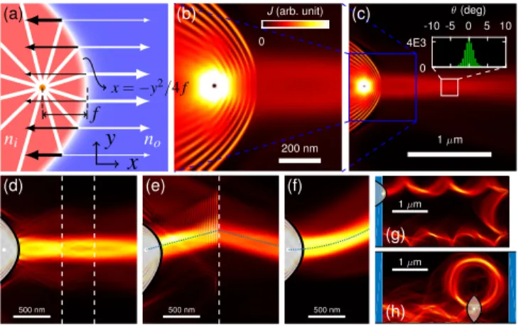
FIG. 1. (a) Schematic of the lensing apparatus composed of a pointlike source at the focal point of a parabolic interface separating two regions with densitiesni and no ¼−ni. (b) An example of the probability current density distribution for design (a), enlarged from (c). Inset in (c): Angle (with respect to thex axis) distribution of the current density analyzed for the white box area. Gallery of panels (d)–(h) showing the electron beam versatility: (d) nearly perfect Klein tunneling, (e) negative re- fraction, (f) bending in a perpendicular magnetic field B, (g)“skipping beam”in theBfield along the edge of a graphene cavity, and (h) beam (from double lens) bent by theBfield to form a full cyclotron orbit. Parameters used: focal lengthf¼ 200nm in (b)–(f),(h) and 100 nm in (g); carrier densityno¼ 6×1011 cm−2in (b)–(g) and7×1011cm−2in (h) (Fermi wave- length≈46and 42 nm, respectively); magnetic fieldB¼40mT in (f) andB¼150mT in (g),(h). Vertical white dashed lines in (d) [(e)] mark an additional potential barrier (step) with densityni.
point. In graphene, the role of the refraction index is played by the Fermi energy relative to the Dirac point and, hence, the carrier density relative to the charge neutrality point. Thus, a parabolic electron lens with individually controllable inner and outer carrier densities ni and no, respectively, can be realized by electrical gating.
Most notably, when ni¼−no, the refracted electron waves are expected not only to collimate into a unidirec- tional wave, but also to concentrate in intensity in a narrow range around the parabola axis due to Klein collimation [23], i.e., the perfect transmission probability across thepn junction at normal incidence, known as the Klein tunneling [26,27], rapidly decreases with an increasing angle of incidence. This combined effect generates a highly direc- tional electron beam with a width of the order of the parabola focal lengthf. This is illustrated in Fig. 1(b)by the local probability current density for f¼200nm.
Throughout the Letter, we refer to the parabolicpnjunction with densitiesni¼−nocombined with a pointlike source at its focal point as the lensing apparatus.
The probability current density images are obtained by the real-space Green’s function method in the tight-binding framework[28]. On siteμatðxμ; yμÞ, the local probability current density at energyE is given by the sum over the bond current vectors to the nearest neighboring sites:
JðE;xμ; yμÞ ¼ X
ν∈n:n:Jμ→νðEÞeμ→ν; ð1Þ witheμ→ν the unit vector pointing from μ toν, and
Jμ→νðEÞ ¼ vF
4πS½G<μ;νðEÞ−G<ν;μðEÞ ð2Þ can be expressed in terms of the lesser Green’s function matrix G<. In noninteracting systems, with the incoming wave sent from one single lead described by self-energyΣi, G<is given by the kinetic equationG<ðEÞ ¼GrðEÞ½Σ†iðEÞ−
ΣiðEÞGaðEÞ, whereGrðaÞis the retarded (advanced) Green’s function of the scattering region.
To treat micron-scale graphene samples, we use a scalable tight-binding model[29], with a scaling factorsf ¼8. This scales the lattice spacing to a∼1nm, enabling us to treat (i) the density range of the order of1012 cm−2, typical for experiments using hBN-encapsulated graphene [30], and (ii) a sharp pn interface of smoothness ∼30nm≫a, a typical thickness of hBN encapsulation layers[4,31]. Note that the prefactor in Eq.(2)containing the Fermi velocityvF and the unit area S¼3 ffiffiffi
p3
a2=4 is irrelevant for current density imaging, since only dimensionless profiles are shown. In our simulations, the pointlike injector diameter will be fixed as 25 nm, not too far from the present technical limit [22].
The presented local current density profiles refer to the magnitude Jðx; yÞ ¼ ½J2xðx; yÞ þJ2yðx; yÞ1=2 of Eq. (1), with the Fermi energy set toE¼0and the on-site energy
profiles obtained from the carrier density profiles described in Ref.[29]. Figure1(c)highlights the unique characteristic of the generated electron wave pertaining to its narrow shape over micron scales. To quantify the high degree of beam collimation, the inset in Fig. 1(c) shows the angle distribution histogram of the azimuthal angle θ¼ arg½Jxðxμ; yμÞ þiJyðxμ; yμÞ for sites μ within the white box area (with totally 80 800 sites). The angle distribution width is as narrow as∼5°. Note that the beam generated by a perfect parabolicpnjunction in the clean limit considered in Fig.1(c), as well as the rest of the discussion, is robust against disorder, as long as the mean free path is much longer than the focal length, and practically insensitive to the junction edge roughness, if the latter’s length scales are shorter than the Fermi wavelength [31]. In addition, all calculations consider zero temperature, since the lensing mechanism is not expected to be vulnerable to finite temperatures[31].
The gallery of panels Figs. 1(d)–1(h) demonstrates various extraordinary properties of the focused electron beam: In Fig. 1(d), an additional barrier (white dashed lines) with the density gated to −no is considered. The collimated wave tunnels through the barrier almost reflec- tionlessly, a consequence of Klein tunneling due to the normal incidence of the beam. In Fig.1(e), an additional potential step (right of the white dashed line) with the density gated to −no results in a symmetrically and negatively refracted electron beam (injected from a lensing apparatus tilted by 15°) as clearly visible from the current density; the blue dotted line marks the expected trajectory in the ray optical limit. The collimation persists also in the presence of a weak perpendicular magnetic field, B¼ ð0;0; BÞ, where “weak” means that the resulting cyclotron radius rc ¼ℏ ffiffiffiffiffiffiffiffiffiffi
πjnoj
p =eB≫f. This is clearly seen in Fig.1(f), the blue dotted line marking the expected cyclotron trajectory segment.
This close correspondence between the quantum mechanical wave propagation and classical cyclotron motion is further illustrated in Figs.1(g) and1(h), where blue patches represent transparent semi-infinite leads. The lensing apparatus in the upper left corner of a graphene cavity, shown in Fig. 1(g), generates a “skipping wave”
that tracks a classical skipping orbit, composed of many cyclotron segments along the top, right, and bottom edges that amount to a length of about 10μm. Skipping orbits are often considered as the classical analogue of quantum Hall edge channels, albeit in a loose sense. Here, the electron beam represents a particular solution to the Schrödinger equation that probably can be regarded as maximally classical, though still subject to interference.
Correspondingly, the ring wave mimicking a full cyclotron orbit, depicted in Fig.1(h)where a double-sided parabolic lens is considered, encloses an Aharonov-Bohm flux.
The ability to both generate such narrow beams and steer their direction through bending in a B field, with high
angular resolution and without losing collimation, immedi- ately opens up the possibility to substantially improve two prominent applications in ballistic graphene electronics, to be described in the following.
First, it enables one to accurately measure the angle- resolved transmission of carriers traversing apn junction, i.e., angle-dependent Klein tunneling, which has remained a long-standing experimental challenge despite some recent efforts[36,37]. Using the proposed lensing apparatus, the angle of incidence can be continuously varied by tuning the Bfield, which bends the electron beam. To simulate such an angle-resolved transmission “experiment,” we perform a transport calculation considering the geometry in Fig.2(a).
There, the transparent drain leads labeled by d are to suppress boundary effects from the finite-size graphene lattice. After traversing a distancelalong the parabola axis, a bent trajectory hits the interface under an angle (with respect to its normal)
ϕ¼arcsin eBl ℏ ffiffiffiffiffiffiffiffiffiffi
πjnoj
p ; ð3Þ
which can be controlled by the field strength B and density no.
Figure 2(b) shows the transmission T for charge flow from the source s to the collector c as a function of magnetic field B and density no by varying the density inside the lens ni¼−no accordingly and fixing nc¼−6×1011 cm−2at the collector.TðϕÞin Fig.2(c)is obtained by takingTðBÞalong the white dashed line cut in Fig.2(b)and usingϕðBÞgiven by Eq.(3). Since along this cut the sharppnjunction between the scattering region and the collector lead becomes symmetric (no¼−nc), the transmission function is expected to behave like a cosine
squared[23]. As seen in Fig. 2(c), the normalized TðϕÞ indeed agrees well with cos2ϕ. As a reference line,TðϕÞ for nc¼no¼6×1011 cm−2 is also shown in Fig. 2(c), exhibiting a nearlyϕ-independent form. BothTðϕÞcurves withnc ¼−no and nc¼no exhibit a small kink around ϕ≈45°, which is simply a boundary (finite size) effect.
By either shorteninglor increasing the width, it is possible to investigateTðϕÞ up to higher angles.
Second, controlled bending of the narrow electron beam is also particularly suited to improve transverse magnetic focusing (TMF). Very recently, TMF in high-mobility graphene has gained strong experimental interest[15–19]
as a tool to study and engineer charge carrier flow. TMF requires that the carrier density fulfills
n¼1 π
eB
h D
j 2
; ð4Þ
wherejis a positive integer andDis the distance between the midpoints of a source and a collector probe. Here we consider a2-μm-wide graphene sample [see the left inset in Fig.3(a)] with the right side attached to a transparent lead (d), such that the sample becomes semi-infinite, and the left side attached to two probes of widthw¼0.4μm, one source (s) and one collector (c), separated by D¼ 1.6μm from each other. We consider only transmission froms to cfor a two-point measurement, rather than the
FIG. 2. (a) Schematic of the lensing apparatus in the presence of a weak magnetic Bfield. (b) TransmissionT for electron flow from the point source (s) to the collector (c) as a function of the field strength and densitynooutside the lens. The density is set to ni¼−noinside the lens and fixed atnc¼−6×1011 cm−2inc. Along the white dashed line,TðBÞnormalized to its maximum is reinterpreted as TðϕÞ in (c), with ϕðBÞ given by Eq.(3), and compared to cos2ϕ(black dashed curve). As a reference curve, TðϕÞwithnc¼no is also shown.
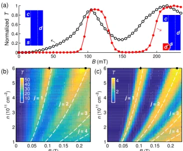
FIG. 3. (a) Normalized transmission T from source s to collectorcas a function of B at densityn¼6×1011 cm−2 in the TMF geometry, without (left inset, black curve) and with (right inset, red curve) the lensing apparatus [similar to Fig.2(a)]
at the lower left terminal. (b) [(c)] Color maps of transmission TðB; nÞ (not normalized) without (with) the lensing apparatus.
TMF states forj¼1;…;4predicted by Eq.(4) are marked by white dashed lines. Symbols diamond and square in (b) and (c) mark the values ofBandnused in Fig.4.
six conductance coefficients required for the four-point resistance [28].
For fixed density n¼6×1011 cm−2, the normalized transmissionTðBÞis shown by the black curve with open circles in Fig.3(a), with two broad peaks corresponding to j¼1andj¼2in line with Eq.(4). Replacing the probes by the lensing apparatus with f¼100nm [right inset in Fig.3(a)], the normalized TðBÞis shown by the red curve with solid dots in Fig.3(a). The lensing apparatus clearly sharpens the TMF signal by narrowing down the j¼1 peak width. Most notably, outside the peak, TðBÞ drops drastically to zero, implying a perfect peak-to-background ratio, as a result of the sharp curved electron beam. In fact, the first TMF peak with lensing occurs roughly between B¼0.1T and B¼0.13T, corresponding to cyclotron diameters of 2rc≈1.81μm and 2rc≈1.39μm, respec- tively. The difference ≈0.42μm agrees well with the collector probe width of w¼0.4μm, again suggesting a highly concentrated electron beam. In Fig.3(b)[3(c)], we show TðB; nÞ color maps without (with) the lensing apparatus; the latter clearly exhibits enhanced j¼1, 2 TMF peaks.
Finally, we consider and simulate scanning gate micros- copy (SGM) as a tool to monitor charge carrier flow. In SGM experiments, a capacitively coupled charged tip is scanned over a phase-coherent sample, thus acting as a tunable and movable scatterer, and the sample conductance (or resistance in four-point measurements) is measured as a function of the tip positionrtip. The differenceΔGðrtipÞ≡ GðrtipÞ−G0between the sample conductance with (G) and without (G0) the tip is plotted as a function of rtip. The images thus obtained were originally interpreted as maps of the coherent electron flow through quantum point contacts defined in two-dimensional electron gases (2DEGs)[38]:
Backscattering from the tip in a region where a lot of electrons are passing by will cause a sizable conductance change, the contrary holding true when the tip is positioned away from such“high flow” regions.
Previous theoretical and experimental works considering a variety of phase-coherent systems [39–51] showed the versatility of this technique but also that a general inter- pretation of an SGM image as a flow map can be problematic [42,43,46,47]. In particular, it was shown in Refs. [43,46] that an explicit connection between local current densities and SGM images requires stringent symmetry conditions. This is consistent with measurements in 2DEG mesoscopic rings [41,42], which established a connection between the local density of states and theΔG images, as well as with recent theoretical[48]and exper- imental[47]developments.
In this context, the lensing apparatus is an ideal tool for testing the interpretation of SGM measurements. For the TMF geometry considered in Fig.3, we compare in Fig.4 the calculated SGM images ΔT and probability current density maps Jðx; yÞ, without [Figs. 4(a)–4(d)] and
with [Figs. 4(e)–4(h)] the lensing apparatus. Here, ΔTðx; yÞ≡½Tðx; yÞ−T0=T0, where T0 without the per- turbing tip has been shown in Figs.3(b)and3(c)andTðx; yÞ is the transmission function from s to c in the presence of a tip at rtip ¼ ðx; yÞ inducing a local carrier density change modeled byntipðx;yÞ¼n0tiph3ðx2þy2þh2Þ−3=2with n0tip ¼−5×1011 cm−2 and h¼50nm adopted from Ref.[18].
Our three-terminal sample does not meet any particular symmetry requirement, and therefore we do not expect a clear correlation between the local current densities and the SGM maps [46]. This is confirmed by Figs. 4(a)–4(d):
Electrons injected into the system generate complex current patterns extending over most of the sample [Figs. 4(b) and4(d)], which are barely reflected by the SGM images [Figs.4(a)and4(c)]—note that the latter agree with recent measurements on graphene[17,18]. The lensing apparatus drastically changes the picture. In Figs.4(f) and4(h), the current densities focus as narrow beams and agree very well with the expected classical trajectories, in sharp contrast to the case without the lensing apparatus. Moreover, the SGM maps in the presence of the lensing apparatus [Figs.4(e) and4(g)] also show a highly concentrated beam structure that agrees well with the classical trajectories. In other words, the SGM signal and the local current density carry the same information. As a consequence, the system response to the local tip perturbation can be unambiguously interpreted classically in terms of the local current flow.
In conclusion, we proposed an efficient collimation mechanism to generate narrow, nondispersive charge car- rier beams in graphene, which can be steered by magnetic fields without losing collimation. The lens allows unprec- edented control over the electron propagation in ballistic FIG. 4. Scanning gate images ΔTðx; yÞ without (with) the lensing apparatus for (a) [(e)] j¼1 and (c) [(g)] j¼2 TMF states, and their corresponding probability current density dis- tributionJðx; yÞfor (b) [(f)]j¼1and (d) [(h)]j¼2. Values of magnetic fieldBand carrier densitynused in (a),(b),(e),(f) and (c),(d),(g),(h) correspond to diamond and square marked in Fig.3, respectively.
graphene, as demonstrated by the example applications of angle-resolved transmission across a pn junction, trans- verse magnetic focusing, and imaging of the current flow simulating scanning gate microscopy. We expect to excite next-generation graphene electron optics experiments based on the proposed concept for wave collimation. As the underlying mechanism exploits negative refraction and Klein collimation that are unique to pseudorelativistic Dirac materials, the lensing mechanism may equally apply to surface states of topological insulators.
We thank C. Handschin, P. Makk, and P. Rickhaus for sharing their opinion about experimental feasibility and R.
Rückner for technical support and system maintenance of Rechenzentrum Universität Regensburg, where most of the presented calculations were performed. Financial support by DFG within SFB 689 is gratefully acknowledged.
*minghao.liu.taiwan@gmail.com
[1] A. F. Young and P. Kim,Nat. Phys.5, 222 (2009).
[2] P. Rickhaus, R. Maurand, M.-H. Liu, M. Weiss, K. Richter, and C. Schönenberger,Nat. Commun.4, 2342 (2013).
[3] A. L. Grushina, D.-K. Ki, and A. F. Morpurgo,Appl. Phys.
Lett.102, 223102 (2013).
[4] C. Handschin, P. Makk, P. Rickhaus, M.-H. Liu, K.
Watanabe, T. Taniguchi, K. Richter, and C. Schönenberger, Nano Lett.17, 328 (2017).
[5] L. Ponomarenkoet al.,Nature (London)497, 594 (2013).
[6] C. Deanet al.,Nature (London)497, 598 (2013).
[7] W. Yang, X. Lu, G. Chen, S. Wu, G. Xie, M. Cheng, D.
Wang, R. Yang, D. Shi, K. Watanabe, T. Taniguchi, C.
Voisin, B. Plaçais, Y. Zhang, and G. Zhang,Nano Lett.16, 2387 (2016).
[8] T. Taychatanapat, J. Y. Tan, Y. Yeo, K. Watanabe, T.
Taniguchi, and B. Özyilmaz,Nat. Commun.6, 6093 (2015).
[9] P. Rickhaus, P. Makk, M.-H. Liu, E. Tóvári, M. Weiss, R.
Maurand, K. Richter, and C. Schönenberger,Nat. Commun.
6, 6470 (2015).
[10] P. Rickhaus, M.-H. Liu, P. Makk, R. Maurand, S. Hess, S.
Zihlmann, M. Weiss, K. Richter, and C. Schönenberger, Nano Lett.15, 5819 (2015).
[11] M. Kim, J.-H. Choi, S.-H. Lee, K. Watanabe, T. Taniguchi, S.-H. Jhi, and H.-J. Lee,Nat. Phys.12, 1022 (2016).
[12] G.-H. Lee, G.-H. Park, and H.-J. Lee,Nat. Phys. 11, 925 (2015).
[13] V. E. Calado, S. Goswami, G. Nanda, M. Diez, A. R.
Akhmerov, K. Watanabe, T. Taniguchi, T. M. Klapwijk, and L. M. K. Vandersypen, Nat. Nanotechnol. 10, 761 (2015).
[14] M. B. Shalom, M. J. Zhu, V. I. Fal’ko, A. Mishchenko, A. V.
Kretinin, K. S. Novoselov, C. R. Woods, K. Watanabe, T.
Taniguchi, A. K. Geim, and J. R. Prance,Nat. Phys.12, 318 (2016).
[15] T. Taychatanapat, K. Watanabe, T. Taniguchi, and P. Jarillo- Herrero,Nat. Phys.9, 225 (2013).
[16] V. E. Calado, S.-E. Zhu, S. Goswami, Q. Xu, K. Watanabe, T. Taniguchi, G. C. A. M. Janssen, and L. M. K. Vandersypen, Appl. Phys. Lett.104, 023103 (2014).
[17] S. Morikawa, Z. Dou, S.-W. Wang, C. G. Smith, K.
Watanabe, T. Taniguchi, S. Masubuchi, T. Machida, and M. R. Connolly,Appl. Phys. Lett.107, 243102 (2015).
[18] S. Bhandari, G.-H. Lee, A. Klales, K. Watanabe, T.
Taniguchi, E. Heller, P. Kim, and R. M. Westervelt,Nano Lett.16, 1690 (2016).
[19] M. Lee, J. R. Wallbank, P. Gallagher, K. Watanabe, T.
Taniguchi, V. I. Fal’ko, and D. Goldhaber-Gordon,Science 353, 1526 (2016).
[20] Although most such experiments were done on exfoliated graphene samples, ballistic transport has also been demon- strated using graphene grown by chemical vapor deposition [16,21].
[21] L. Banszerus, M. Schmitz, S. Engels, M. Goldsche, K.
Watanabe, T. Taniguchi, B. Beschoten, and C. Stampfer, Nano Lett.16, 1387 (2016).
[22] C. Handschin, B. Fülöp, P. Makk, S. Blanter, M. Weiss, K.
Watanabe, T. Taniguchi, S. Csonka, and C. Schönenberger, Appl. Phys. Lett.107, 183108 (2015).
[23] V. V. Cheianov and V. I. Fal’ko,Phys. Rev. B74, 041403 (2006).
[24] C.-H. Park, Y.-W. Son, L. Yang, M. L. Cohen, and S. G.
Louie, Nano Lett.8, 2920 (2008).
[25] E. Hecht,Optics(Pearson Education, Upper Saddle River, NJ, 2015).
[26] O. Klein,Z. Phys.53, 157 (1929).
[27] M. I. Katsnelson, K. S. Novoselov, and A. K. Geim, Nat.
Phys.2, 620 (2006).
[28] S. Datta, Electronic Transport in Mesoscopic Systems (Cambridge University Press, Cambridge, England, 1995).
[29] M.-H. Liu, P. Rickhaus, P. Makk, E. Tóvári, R. Maurand, F.
Tkatschenko, M. Weiss, C. Schönenberger, and K. Richter, Phys. Rev. Lett.114, 036601 (2015).
[30] C. R. Dean, A. F. Young, I. Meric, C. Lee, L. Wang, S.
Sorgenfrei, K. Watanabe, T. Taniguchi, P. Kim, K. L.
Shepard, and J. Hone,Nat. Nanotechnol.5, 722 (2010).
[31] See Supplemental Material at http://link.aps.org/
supplemental/10.1103/PhysRevLett.118.066801 for numerical examples about potential disorder in graphene samples, edge roughness of the parabolic gate, and smooth- ness of thepnjunction and a brief discussion about finite temperature, which includes Refs. [32–35].
[32] D. K. Ferry, S. M. Goodnick, and J. Bird, Transport in Nanostructures (Cambridge University Press, Cambridge, England, 2009).
[33] T. Fang, A. Konar, H. Xing, and D. Jena,Phys. Rev. B78, 205403 (2008).
[34] A. Yazdanpanah, M. Pourfath, M. Fathipour, H. Kosina, and S. Selberherr,IEEE Trans. Electron Devices59, 433 (2012).
[35] L. Wang, I. Meric, P. Y. Huang, Q. Gao, Y. Gao, H. Tran, T.
Taniguchi, K. Watanabe, L. M. Campos, D. A. Muller, J.
Guo, P. Kim, J. Hone, K. L. Shepard, and C. R. Dean, Science342, 614 (2013).
[36] S. Sutar, E. S. Comfort, J. Liu, T. Taniguchi, K. Watanabe, and J. U. Lee,Nano Lett.12, 4460 (2012).
[37] A. Rahman, J. W. Guikema, N. M. Hassan, and N. Marković, Appl. Phys. Lett.106, 013112 (2015).
[38] M. A. Topinka, B. J. LeRoy, R. M. Westervelt, S. E. J. Shaw, R. Fleischmann, E. J. Heller, K. D. Maranowski, and A. C.
Gossard,Nature (London)410, 183 (2001).
[39] M. T. Woodside and P. L. McEuen, Science 296, 1098 (2002).
[40] K. E. Aidala, R. E. Parrott, T. Kramer, E. Heller, R.
Westervelt, M. P. Hanson, and A. C. Gossard, Nat. Phys.
3, 464 (2007).
[41] F. Martins, B. Hackens, M. G. Pala, T. Ouisse, H. Sellier, X.
Wallart, S. Bollaert, A. Cappy, J. Chevrier, V. Bayot, and S.
Huant,Phys. Rev. Lett.99, 136807 (2007).
[42] M. G. Pala, B. Hackens, F. Martins, H. Sellier, V. Bayot, S. Huant, and T. Ouisse, Phys. Rev. B 77, 125310 (2008).
[43] R. A. Jalabert, W. Szewc, S. Tomsovic, and D. Weinmann, Phys. Rev. Lett.105, 166802 (2010).
[44] S. Schnez, J. Güttinger, C. Stampfer, K. Ensslin, and T. Ihn, New J. Phys.13, 053013 (2011).
[45] N. Paradiso, S. Heun, S. Roddaro, L. Sorba, F. Beltram, G.
Biasiol, L. N. Pfeiffer, and K. W. West,Phys. Rev. Lett.108, 246801 (2012).
[46] C. Gorini, R. A. Jalabert, W. Szewc, S. Tomsovic, and D.
Weinmann,Phys. Rev. B88, 035406 (2013).
[47] A. A. Kozikov, D. Weinmann, C. Rössler, T. Ihn, K. Ensslin, C. Reichl, and W. Wegscheider, New J. Phys.15, 083005 (2013).
[48] K. Kolasiński and B. Szafran,New J. Phys.16, 053044 (2014).
[49] N. Aoki, C. R. da Cunha, R. Akis, D. K. Ferry, and Y.
Ochiai,J. Phys. Condens. Matter26, 193202 (2014).
[50] A. A. Zhukov, C. Volk, A. Winden, H. Hardtdegen, and T.
Schäpers, J. Phys. Condens. Matter26, 165304 (2014).
[51] A. Kleshchonok, G. Fleury, J.-L. Pichard, and G. Lemarié, Phys. Rev. B91, 125416 (2015).