Ming-Hao Liu (劉明豪),∗ Cosimo Gorini, and Klaus Richter
Institut f¨ur Theoretische Physik, Universit¨at Regensburg, D-93040 Regensburg, Germany (Dated: August 8, 2016)
An electron collimator composed of a point-like source and a parabolicpnjunction is proposed as a generator of highly focused electron beams in graphene. The collimator is based on negative refraction and Klein colli- mation, which are unique to pseudo-relativistic Dirac materials. The electron beams generated by the lensing apparatus can be steered by a weak magnetic field without losing collimation, which makes the parabolic lens a flexible platform for next-generation graphene electron optics experiments. This is shown by a few example ap- plications concerning angle-resolved transmission at apnjunction, transverse magnetic focusing, and mapping of the current flow in scanning gate microscopy.
PACS numbers: 72.80.Vp, 72.10.-d, 73.23.Ad
Ballistic charge transport of Dirac fermions has recently been an emerging hot topic in graphene electronics, thanks not only to the rapidly improving sample quality but also to the highly intertwined theoretical and experimental efforts.
Accordingly, over the past few years, novel transport behav- iors of electrons in single-layer graphene have been reported, such as Fabry-P´erot interference [1–3], Hofstadter butterfly in exfoliated graphene on hexagonal boron nitride (hBN) [4,5]
and in epitaxial graphene grown on hBN [6], snake states along pn junctions [7,8], gate-defined electron wave guide [9,10], negative refraction [11], ballistic Josephson junction [12,13], transverse magnetic focusing [14–16], and imaging of their cyclotron trajectories using scanning gate microscopy [17, 18]. Although most of such experiments were done on exfoliated graphene samples, ballistic transport has also been demonstrated using CVD (chemical vapor deposition) graphene [15,19].
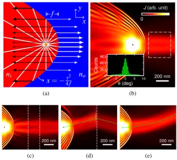
Despite the stunning progress of quantum transport experi- ments and simulations in recent years, decent control of elec- tron wave propagation in graphene is still limited. Whereas electrons in graphene behave like “charged photons” that ex- hibit both electronic and optical properties, the lack of a nar- row beam source hinders the development of graphene elec- tron optics. Motivated by the recent work on point contacts of hBN-encapsulated graphene byHandschinet al.[20], here we propose a simple and efficient electron collimator for point sources in graphene, exploiting negative refraction unique to Dirac materials. Contrary to Klein collimation [21] or super- collimation in superlattices [22], we consider a paraboloidpn junction with a point-like source located at its focal point; see Fig.1(a).
Paraboloidals are known to have a wide variety of applica- tions, ranging from flashlight reflectors to radiotelescope an- tennas [23], where either a wave emitted from a point source is turned into a plane wave by specular reflection [black arrows in Fig.1(a)], or vice versa. For a point source of waves tore- fracttoward an identical direction parallel to the parabola axis [white arrows in Fig.1(a)], on the other hand, the refraction indices inside and outside the paraboloid must be of oppo- site sign, provided that the point source is located at the focal point. In graphene, the role of the refraction index is played
by the Fermi energy relative to the Dirac point, and hence the carrier density relative to the charge neutrality point. Thus a paraboloidal electron lens with individually controllable inner and outer carrier densitiesni,nocan be realized by electrical gating.
Most notably, whenni=−no, the refracted electron waves are expected not only to collimate into a unidirectional wave, but also to concentrate in intensity in a narrow range around the parabola axis due to Klein collimation [21], i.e., the perfect
f
ni no
y x
x=−4fy2 (a)
200 nm J (arb. unit) 0
θ (deg)
Counts
−100 −5 0 5 10 3E3
6E3 9E3
(b)
200 nm
(c)
200 nm
(d)
200 nm
(e)
FIG. 1. (a) Schematic of the lensing apparatus composed of a point source at the focal point of a parabolic interface separating two re- gions with densitiesniandno=−ni. (b) An example of the proba- bility current density distribution due to the lensing apparatus, gen- erating a narrow, collimated electron beam, which shows (c) nearly perfect Klein tunneling, (d) negative refraction, and (e) bending in the presence of a weak magnetic fieldB=40mT. Focal length f=200nm and carrier densitiesno=6×1011cm−2=−ni(Fermi wavelength≈46nm) are considered in (b)–(e). Vertical white dashed lines in (c)/(d) mark an additional potential barrier/step. Green dashed lines in (d) and (e) denote the expected trajectories. Inset in (b): angle distribution (defined with respect tox-axis) of the current density analyzed for the area marked by the white dashed box.
arXiv:1608.01730v1 [cond-mat.mes-hall] 5 Aug 2016
transmission probability across thepnjunction at normal inci- dence, known as the Klein tunneling [24,25], decreases with the increasing angle of incidence. This combined effect gen- erates a non-dispersive electron beam with width of the order of the paraboloid focal lengthf. This is illustrated in Fig.1(b) by the local probability current density for f=200nm. In the rest of the paper, we refer to the parabolicpnjunction with densities ni=−no combined with a point-like source at its focal point as the lensing apparatus.
The probability current density images presented are ob- tained by the real-space Green’s function method in the tight- binding framework [26]. At siteµat(xµ,yµ), the local proba- bility current density at energyEis given by the sum over the bond current vectors to the nearest neighboring sites,
J(E;xµ,yµ) =
∑
ν∈n.n.Jµ→ν(E)eµ→ν, (1) whereeµ→νis the unit vector pointing fromµtoν, and
Jµ→ν(E) = vF
4πS[G<µ,ν(E)−G<ν,µ(E)] (2) can be expressed in terms of the Keldysh Green’s function matrix G<. In noninteracting systems, with the incoming wave sent from one single lead described by self-energyΣi, the Keldysh Green’s function is given by the kinetic equation G<(E) =Gr(E)[Σ†i(E)−Σi(E)]Ga(E), whereGr/ais the re- tarded/advanced Green’s function of the scattering region.
To treat micron-scale graphene samples, we use the scal- able tight-binding model for graphene [27], and adopt a scal- ing factorsf =8. This scales the lattice spacing toa∼1nm, enabling us to treat (i) the density range of the order of 1012cm−2, typical for experiments using hBN-encapsulated graphene [28], and (ii) a sharp pn interface of smoothness
∼30nma, typical thickness of hBN encapsulation layers.
Note that the prefactor in Eq. (2) containing the Fermi veloc- ityvF and the unit areaS=3√
3a2/4 is irrelevant for current density imaging since only dimensionless profiles are shown.
In our simulations, the diameter of the point-like injector [29]
will be fixed as 25nm for convenience, which is not too far from the present technical limit [20].
The local current density profiles shown in this work refer to the magnitudeJ(x,y) = [Jx2(x,y) +Jy2(x,y)]1/2of Eq. (1), with the Fermi energy set to E=0 and the on-site energy profiles obtained from the carrier density profiles described in Ref.27. To further quantify the degree of electron beam colli- mation depicted in Fig.1(b), the inset shows the angle distri- bution histogram of the azimuthal angleθ=arg[Jx(xµ,yµ) + iJy(xµ,yµ)]for sites µ within the area marked by the white dashed box (with totally 80800 sites). The peak width of the angle distribution, as narrow as∼5◦, shows a highly colli- mated electron beam.
The gallery of panels Fig.1(c)–1(e)demonstrates various properties of the focused electron beam: In Fig.1(c), an ad- ditional barrier (marked by the white dashed lines) with den- sity gated to−nois considered. The collimated beam tunnels through the barrier almost reflectionlessly, a consequence of
d
d d
c s
200 nm
rc
φ
`
ni no nc
(a)
B (mT) no (1012 cm−2)
−100 −50 0 50 100
0.4 0.6 0.8 1 1.2
T 2 3 4
(b)
−45 −30 −15 0 15 30 45
0.4 0.6 0.8 1
φ (deg)
Normalized T
nc = n
o
cos2φ nc = −n
o
(c)
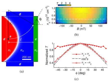
FIG. 2. (a) Schematic of the lensing apparatus in the presence of a weak magneticBfield. (b) TransmissionT for electron flow from the point source (s) to the collector (c) as a function of field strength and densityno outside the lens. The density inside the lens is set toni=−no, and the density in the collector lead is fixed atnc=
−6×1011cm−2. Along the white dashed line,T(B)normalized to its maximum is re-interpreted asT(φ) in (c), withφ(B)given by Eq. (3), and compared to cos2φ(black dashed curve). As a reference curve,T(φ)withnc=nois also shown.
Klein tunneling. In Fig.1(d), an additional potential step (to the right of the white dashed line) with density gated to−no
results in a symmetrically and negatively refracted electron beam which is clearly visible from the current density; the green dashed line marks the expected trajectory in the ray op- tical limit. The collimation generated by the lensing apparatus also works in the presence of a weak perpendicular magnetic field,B= (0,0,B), where “weak” means that the resulting cy- clotron radiusrc=h¯pπ|no|/eB f. This is clearly seen in Fig.1(e), where the green dashed line marks the expected cyclotron trajectory segment.
This fact that the electron beam can be bent by a B field without losing collimation enables one to accurately measure the angle-resolved transmission of electrons traversing apn junction, which has remained an experimental challenge de- spite some recent efforts [30,31]. Using the proposed lens- ing apparatus, the angle of incidence can be continuously var- ied by tuning theBfield, which bends the electron beam to a cyclotron trajectory segment. To simulate such an angle- resolved transmission “experiment”, we perform a transport calculation considering the geometry in Fig.2(a). There, the transparent drain leads labeled bydare to suppress boundary effects from the finite-size graphene lattice. After traversing a distance`along the parabola axis, a bent trajectory hits the interface under an angle (with respect to its normal)
φ=arcsin eB`
h¯pπ|no|, (3) which can be controlled by the field strengthBand densityno. Figure2(b)shows the transmissionT for charge flow from
the sourcesto the collectorcas a function of magnetic fieldB and densitynoby varying the density inside the lensni=−no
accordingly and fixingnc=−6×1011cm−2at the collector.
T(φ)in Fig.2(c)is obtained by takingT(B)along the white dashed line cut in Fig.2(b)and usingφ(B)given by Eq. (3).
Since along this line cut the sharp pnjunction between the scattering region and the collector lead becomes symmetric (no=−nc), the transmission function is expected to behave like a cosine squared [21]. As seen in Fig.2(c), the normal- izedT(φ)indeed agrees well with cos2φ. As a reference line, T(φ)fornc=no=6×1011cm−2is also shown in Fig.2(c), which reasonably exhibits a nearlyφ-independent form. Due to the spatial limit of the considered geometry, both T(φ) curves withnc=−noandnc=noexhibit a small kink around φ≈ ±45◦, which is simply a boundary effect. By either short- ening `or increasing the width, it is possible to investigate T(φ)up to higher angles.
Bending the electron beam in a controllable way makes it also particularly suitable for transverse magnetic focusing (TMF). Very recently, TMF in high-mobility graphene has gained strong experimental interest [14–18] as a tool to study and engineer charge carrier flow. TMF requires that the carrier density fulfills
n=1 π
eB h
D j
2
, (4)
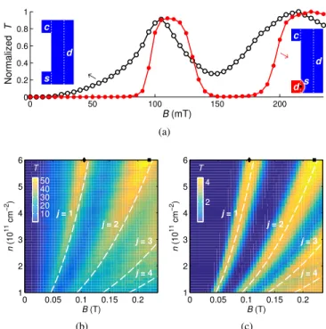
wherejis a positive integer andDis the distance between the midpoints of a source and a collector probe. Here we consider a 2-µm-wide graphene sample [see left inset in Fig.3(a)] with the right side attached to a transparent lead (d), such that the sample becomes semi-infinite, and the left side attached to two probes of widthw=0.4µm, one source (s) and one collector (c), separated byD=1.6µm from each other. We consider only transmission fromstocfor a two-point measurement, instead of all the six conductance coefficients required for the four-point resistance using B¨uttiker formula [26].
For fixed densityn=6×1011cm−2, the normalized trans- missionT(B)is shown by the black curve with open circles in Fig.3(a), with two broad peaks corresponding toj=1 and j=2 in line with Eq. (4). Replacing the probesby the lens- ing apparatus with f =100nm [right inset of Fig.3(a)], the normalized T(B)is shown by the red curve with solid dots in Fig.3(a). The lensing apparatus clearly sharpens the TMF signal by narrowing down the peak width for j=1. Most notably, outside the peak,T(B)drops drastically to zero, im- plying a well defined, curved electron beam. In fact, the first TMF peak with lensing occurs roughly between B=0.1T andB=0.13T, which corresponds to cyclotron diameters of 2rc≈1.81µm and 2rc≈1.39µm, respectively, and the dif- ference≈0.42µm agrees well with the collector probe width ofw=0.4µm, again suggesting a highly concentrated elec- tron beam. In Figs.3(b)/3(c), we showT(B,n)color maps without/with the lensing apparatus; the latter clearly exhibits enhanced j=1,2 TMF peaks.
Finally, we move on to the last example: the scanning gate microscopy (SGM). In SGM experiments, a capacitively cou-
s c
d
ds c
d
0 50 100 150 200
0 0.2 0.4 0.6 0.8 1
B (mT)
Normalized T
←
→
(a)
B (T) n (1011 cm−2)
j = 1
j = 2 j = 3
j = 4 0 0.05 0.1 0.15 0.2 1
2 3 4 5 6
T
10 20 30 40 50
(b)
B (T) n (1011 cm−2)
j = 1
j = 2 j = 3
j = 4 0 0.05 0.1 0.15 0.2 1
2 3 4 5 6
T
2 4
(c)
FIG. 3. Transverse magnetic focusing (TMF). (a) Normalized trans- missionT from sourcesto collectorcas a function ofBat density n=6×1011cm−2 in the TMF geometry, without (left inset, black curve) and with (right inset, red curve) the lensing apparatus [simi- lar to Fig.2(a)] at lower left terminal. (b)/(c) Color maps of trans- missionT(B,n)(not normalized) without/with the lensing apparatus.
TMF states forj=1, . . . ,4 predicted by Eq. (4) are marked by white dashed lines. Values ofBandnmarked byandin (b)/(c) corre- spond to Fig.4(a)/4(c)and Fig.4(b)/4(d), respectively.
pled charged tip is scanned over a phase-coherent sample, thus acting as a tunable and movable scatterer, and the sam- ple conductance (or resistance in four-point measurements) is measured as a function of the tip position rtip. The dif- ference∆G(rtip)≡G(rtip)−G0between the sample conduc- tance with (G) and without (G0) the tip is plotted as a function ofrtip. The images thus obtained were originally interpreted as maps of the coherent electron flow through quantum point contacts defined in two-dimensional electron gases (2DEGs) [32]: Backscattering from the tip in a region where a lot of electrons are passing by will cause a sizeable conductance change, the contrary holding true when the tip is positioned away from such “high flow” regions.
Previous theoretical and experimental works considering a variety of phase-coherent systems [33–45] showed the ver- satility of this technique, but also that a general interpreta- tion of an SGM image as a flow map can be problematic [36,37,40,41]. In particular, it was shown in Refs.37and40 that an explicit connection between local current densities and SGM images requires stringent symmetry conditions. This is consistent with measurements in 2DEGs mesoscopic rings [35, 36], which established a connection between the local density of states and the∆Gimages, as well as with recent theoretical [42] and experimental [41] developments.
x (µm)
y (µm)
s c
0 0.5 1 1.5
−2
−1 0
∆T (%)
−10
−5 0 5 10
x (µm)
y (µm)
s c
0 0.5 1 1.5
−2
−1 0
0
J (arb. unit)
(a)TMF atj=1 without lensing.
x (µm)
y (µm)
s c
0 0.5 1
−2
−1 0
∆T (%)
−10
−5 0 5 10
x (µm)
y (µm)
s c
0 0.5 1
−2
−1 0
0
J (arb. unit)
(b)TMF atj=2 without lensing.
x (µm)
y (µm)
s c
0 0.5 1 1.5
−2
−1 0
∆T (%)
−40
−20 0 20 40
x (µm)
y (µm)
s c
0 0.5 1 1.5
−2
−1 0
0
J (arb. unit)
(c)TMF atj=1 with lensing.
x (µm)
y (µm)
s c
0 0.5 1
−2
−1 0
∆T (%)
−40
−20 0 20 40
x (µm)
y (µm)
s c
0 0.5 1
−2
−1 0
0
J (arb. unit)
(d)TMF atj=2 with lensing.
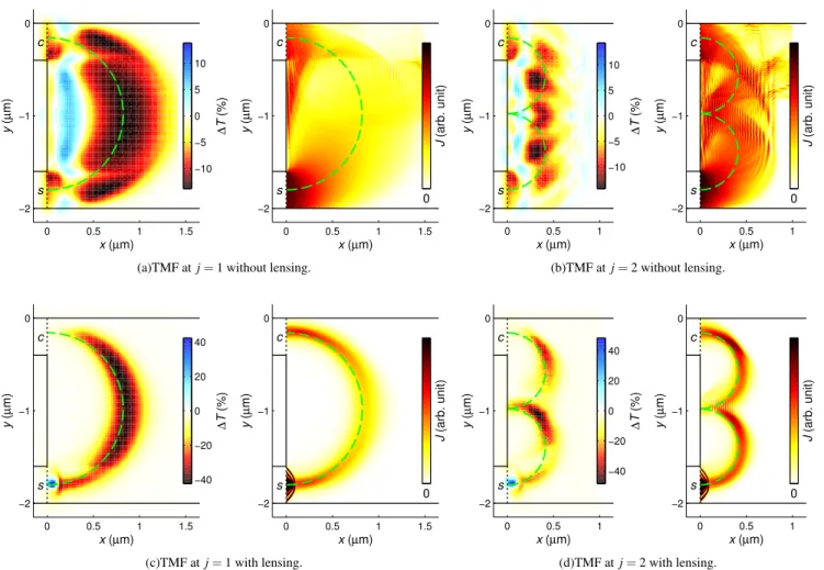
FIG. 4. Scanning gate images∆T(x,y)versus the probability current density distributionJ(x,y)without/with the lensing apparatus for (a)/(c) j=1 and (b)/(d) j=2 TMF states, respectively, with magnetic fieldBand carrier densitynmarked by the solid diamond and solid square in Fig.3(b)/3(c). Green dashed lines in each panel denote the expected classical trajectories in a ray picture.
In this context, the lensing apparatus is an ideal tool for test- ing the interpretation of SGM measurements. For the TMF geometry considered in Fig.3we compare in Fig.4the calcu- lated SGM images∆T and probability current density maps J(x,y), without [Figs.4(a)–4(b)] and with [Figs.4(c)–4(d)]
the lensing apparatus. Here,∆T(x,y) =T(x,y)−T0, where T0 without the perturbing tip has been shown in Figs.3(b)–
3(c)andT(x,y)is the transmission function fromstocin the presence of a tip atrtip= (x,y)inducing a local carrier density change modeled byntip(x,y) =n0tiph3(x2+y2+h2)−3/2with n0tip=−5×1011cm−2andh=50nm adopted from Ref.18.
Our three-terminal sample does not meet any particular symmetry requirement, and therefore we do not expect a clear correlation between the local current densities and the SGM maps [40]. This is confirmed by Figs.4(a)and4(b): electrons injected into the system generate complex current patterns ex- tending over most of the sample [right panels of Figs.4(a)and 4(b)], which are barely reflected by the SGM images – note that the latter agree with recent measurements on graphene [17,18]. The lensing apparatus drastically changes the pic-
ture. In the right panels of Figs.4(c) and 4(d) the current densities focus as narrow beams and agree very well with the expected classical trajectories marked by green dashed lines, in sharp contrast to the case without the lensing apparatus [Figs.4(a)–4(b)]. Moreover, the SGM maps in the presence of the lensing apparatus [left panels of Figs.4(c)and4(d)] also show a highly concentrated beam structure that agrees well with the classical trajectories. In other words, the SGM signal and the local current density carry the same information. As a consequence, the system response to the local tip perturbation can be unambiguously interpreted classically in terms of the local current flow.
In conclusion, the proposed lensing apparatus for graphene has been shown to generate highly collimated, non-dispersive electron beams, which can be steered by a weak magnetic field without losing collimation. As the underlying mecha- nism exploits negative refraction and Klein collimation that are unique to pseudo-relativistic Dirac materials, the lensing mechanism may equally apply to topological insulators. Our lens allows unprecedented control over the electron propaga- tion in ballistic graphene, as demonstrated by the example ap-
plications of angle-resolved transmission across apnjunction, transverse magnetic focusing, and imaging of the current flow using scanning gate microscopy. We expect to excite next- generation graphene electron optics experiments based on the proposed parabolic lens.
We thank P. Rickhaus, P. Makk, and C. Handschin for shar- ing their opinion about experimental feasibility. Financial support by DFG within SFB 689 is gratefully acknowledged.
∗ minghao.liu.taiwan@gmail.com
[1] A. F. Young and P. Kim,Nat. Phys.5, 222 (2009).
[2] P. Rickhaus, R. Maurand, M.-H. Liu, M. Weiss, K. Richter, and C. Sch¨onenberger,Nat. Commun.4, 2342 (2013).
[3] A. L. Grushina, D.-K. Ki, and A. F. Morpurgo,Appl. Phys.
Lett.102, 223102 (2013).
[4] L. Ponomarenko, R. Gorbachev, G. Yu, D. Elias, R. Jalil, A. Pa- tel, A. Mishchenko, A. Mayorov, C. Woods, J. Wallbank,et al., Nature497, 594 (2013).
[5] C. Dean, L. Wang, P. Maher, C. Forsythe, F. Ghahari, Y. Gao, J. Katoch, M. Ishigami, P. Moon, M. Koshino,et al.,Nature 497, 598 (2013).
[6] W. Yang, X. Lu, G. Chen, S. Wu, G. Xie, M. Cheng, D. Wang, R. Yang, D. Shi, K. Watanabe, T. Taniguchi, C. Voisin, B. Plac¸ais, Y. Zhang, and G. Zhang, Nano Lett. 16, 2387 (2016).
[7] T. Taychatanapat, J. Y. Tan, Y. Yeo, K. Watanabe, T. Taniguchi, and B. ¨Ozyilmaz,Nat. Commun.6, 6093 (2015).
[8] P. Rickhaus, P. Makk, M.-H. Liu, E. T´ov´ari, M. Weiss, R. Mau- rand, K. Richter, and C. Sch¨onenberger,Nat. Commun.6, 6470 (2015).
[9] P. Rickhaus, M.-H. Liu, P. Makk, R. Maurand, S. Hess, S. Zihlmann, M. Weiss, K. Richter, and C. Sch¨onenberger, Nano Lett.15, 5819 (2015).
[10] M. Kim, J.-H. Choi, S.-H. Lee, K. Watanabe, T. Taniguchi, S.- H. Jhi, and H.-J. Lee,Nat. Phys. , advance online publication (2016).
[11] G.-H. Lee, G.-H. Park, and H.-J. Lee, Nat. Phys. 11, 925 (2015).
[12] V. E. Calado, S. Goswami, G. Nanda, M. Diez, A. R.
Akhmerov, K. Watanabe, T. Taniguchi, T. M. Klapwijk, and L. M. K. Vandersypen,Nat. Nano.10, 761 (2015).
[13] M. B. Shalom, M. J. Zhu, V. I. Fal’ko, A. Mishchenko, A. V. Kretinin, K. S. Novoselov, C. R. Woods, K. Watanabe, T. Taniguchi, A. K. Geim, and J. R. Prance,Nat. Phys.12, 318 (2016).
[14] T. Taychatanapat, K. Watanabe, T. Taniguchi, and P. Jarillo- Herrero,Nat. Phys.9, 225 (2013).
[15] V. E. Calado, S.-E. Zhu, S. Goswami, Q. Xu, K. Watanabe, T. Taniguchi, G. C. A. M. Janssen, and L. M. K. Vandersypen, Appl. Phys. Lett.104, 023103 (2014).
[16] M. Lee, J. R. Wallbank, P. Gallagher, K. Watanabe, T. Taniguchi, V. I. Fal’ko, and D. Goldhaber-Gordon, ArXiv e-prints (2016),arXiv:1603.01260 [cond-mat.mes-hall].
[17] S. Morikawa, Z. Dou, S.-W. Wang, C. G. Smith, K. Watanabe, T. Taniguchi, S. Masubuchi, T. Machida, and M. R. Connolly, Appl. Phys. Lett.107, 243102 (2015).
[18] S. Bhandari, G.-H. Lee, A. Klales, K. Watanabe, T. Taniguchi, E. Heller, P. Kim, and R. M. Westervelt,Nano Lett.16, 1690 (2016).
[19] L. Banszerus, M. Schmitz, S. Engels, M. Goldsche, K. Watan- abe, T. Taniguchi, B. Beschoten, and C. Stampfer,Nano Letters 16, 1387 (2016).
[20] C. Handschin, B. F¨ul¨op, P. Makk, S. Blanter, M. Weiss, K. Watanabe, T. Taniguchi, S. Csonka, and C. Sch¨onenberger, Appl. Phys. Lett.107, 183108 (2015).
[21] V. V. Cheianov and V. I. Fal’ko, Phys. Rev. B 74, 041403 (2006).
[22] C.-H. Park, Y.-W. Son, L. Yang, M. L. Cohen, and S. G. Louie, Nano Lett.8, 2920 (2008).
[23] E. Hecht,Optics(Pearson Education, 2015).
[24] O. Klein,Zeitschrift f¨ur Physik53, 157 (1929).
[25] M. I. Katsnelson, K. S. Novoselov, and A. K. Geim,Nat. Phys.
2, 620 (2006).
[26] S. Datta,Electronic Transport in Mesoscopic Systems(Cam- bridge University Press, Cambridge, 1995).
[27] M.-H. Liu, P. Rickhaus, P. Makk, E. T´ov´ari, R. Maurand, F. Tkatschenko, M. Weiss, C. Sch¨onenberger, and K. Richter, Phys. Rev. Lett.114, 036601 (2015).
[28] C. R. Dean, A. F. Young, I. Meric, C. Lee, L. Wang, S. Sorgen- frei, K. Watanabe, T. Taniguchi, P. Kim, K. L. Shepard, and J. Hone,Nat. Nano.5, 722 (2010).
[29] The point-like injector is modeled by a self-energy calculated using (i) the cell HamiltonianH0belonging to the block of the Nd sites within the defined disk area of the full Hamiltonian of the considered scaled graphene lattice, and (ii) the hopping HamiltonianH+1 given by anNd×Nd identity matrix multi- plied by−t. For the disk diameter of 25nm considered in all numerical examples of the present work usingsf =8 scaled graphene,Nd=258.
[30] S. Sutar, E. S. Comfort, J. Liu, T. Taniguchi, K. Watanabe, and J. U. Lee,Nano Lett.12, 4460 (2012).
[31] A. Rahman, J. W. Guikema, N. M. Hassan, and N. Markovi´c, Appl. Phys. Lett.106, 013112 (2015).
[32] M. A. Topinka, B. J. LeRoy, R. M. Westervelt, S. E. J. Shaw, R. Fleischmann, E. J. Heller, K. D. Maranowski, and A. C.
Gossard,Nature410, 183 (2001).
[33] M. T. Woodside and P. L. McEuen,Science296, 1098 (2002).
[34] K. E. Aidala, R. E. Parrott, T. Kramer, E. Heller, R. Westervelt, M. P. Hanson, and A. C. Gossard,Nat. Phys.3, 464 (2007).
[35] F. Martins, B. Hackens, M. G. Pala, T. Ouisse, H. Sellier, X. Wallart, S. Bollaert, A. Cappy, J. Chevrier, V. Bayot, and S. Huant,Phys. Rev. Lett.99, 136807 (2007).
[36] M. G. Pala, B. Hackens, F. Martins, H. Sellier, V. Bayot, S. Huant, and T. Ouisse,Phys. Rev. B77, 125310 (2008).
[37] R. A. Jalabert, W. Szewc, S. Tomsovic, and D. Weinmann, Phys. Rev. Lett.105, 166802 (2010).
[38] S. Schnez, J. G¨uttinger, C. Stampfer, K. Ensslin, and T. Ihn, New J. Phys.13, 053013 (2011).
[39] N. Paradiso, S. Heun, S. Roddaro, L. Sorba, F. Beltram, G. Bi- asiol, L. N. Pfeiffer, and K. W. West,Phys. Rev. Lett.108, 246801 (2012).
[40] C. Gorini, R. A. Jalabert, W. Szewc, S. Tomsovic, and D. Wein- mann,Phys. Rev. B88, 035406 (2013).
[41] A. A. Kozikov, D. Weinmann, C. R¨ossler, T. Ihn, K. Ensslin, C. Reichl, and W. Wegscheider, New J. Phys. 15, 083005 (2013).
[42] K. Kolasi`nski and B. Szafran,New J. Phys.16, 053044 (2014).
[43] N. Aoki, C. R. da Cunha, R. Akis, D. K. Ferry, and Y. Ochiai, J. Phys: Condens. Matter26, 193202 (2014).
[44] A. A. Zhukov, C. Volk, A. Winden, H. Hardtdegen, and T. Sch¨apers,J. Phys.: Condens. Matter26, 165304 (2014).
[45] A. Kleshchonok, G. Fleury, J.-L. Pichard, and G. Lemari´e, Phys. Rev. B91, 125416 (2015).