Charge and spin transport in carbon nanotubes:
From Coulomb blockade to FabryPerot interference
DISSERTATION ZUR ERLANGUNG DES DOKTORGRADES DER NATURWISSENSCHAFTEN (DR. RER . NAT . ) DER FAKULTÄT FÜR PHYSIK
DER UNIVERSITÄT REGENSBURG
vorgelegt von
Alois Roman Dirnaichner
aus
Wasserburg am Inn
im Jahr 2016
Promotionsgesuch eingereicht am:
2.7.2015
Die Arbeit wurde angeleitet von:
Prof. Christoph Strunk
Prüfungsausschuss:
Vorsitzender: Prof. Dr. F. Gießibl 1. Gutachter: Prof. Dr. C. Strunk 2. Gutachter: Prof. Dr. M. Grifoni weiterer Prüfer: Prof. Dr. V. Braun
Termin Promotionskolloquium: 27.4.2016
Contents
I Introduction 7
II Tunneling magneto-resistance in a carbon nan-
otube quantum dot 13
1 Introduction to quantum dot transport in the Coulomb block-
ade regime 15
1.1 Quantum dot spectroscopy . . . . 17
1.2 A carbon nanotube quantum dot . . . . 21
1.2.1 The graphene dispersion relation . . . . 21
1.2.2 The carbon nanotube dispersion relation . . . . 23
1.2.3 The single electron transport spectrum of a carbon nanotube quantum dot . . . . 28
2 Modeling a CNT quantum dot coupled to ferromagnetic leads 37 2.1 Introduction to the reduced density matrix approach . . . . . 38
2.1.1 Statistical mixtures . . . . 38
2.1.2 Time evolution of statistical mixtures . . . . 40
2.1.3 The reduced density matrix . . . . 41
2.1.4 The Laplace transform of the Kernel . . . . 47
2.1.5 Electronic transport . . . . 49
2.1.6 Remarks on the reduced density matrix approach . . . 50
2.2 The dressed second order approach applied to a CNT quantum dot . . . . 51
2.2.1 The Hamiltonian of the system . . . . 54
2.2.2 Lowest (second) order in the coupling . . . . 57
2.2.3 The dressed-second order series . . . . 59
2.2.4 Effects of magnetization on resonance width . . . . 67
2.3 Application to experimental data: TMR of a CNT quantum dot 70 2.3.1 Experiment . . . . 72
2.3.2 Measurement . . . . 73
2.3.3 Comparison between experiment and model output . . 77
2.4 Summary & Outlook . . . . 80
Appendices 83 2.A Transformation of Eq. (2.22) to the Schrödinger picture . . . . 83
2.B Fabrication parameters of CB3224 . . . . 84
2.C Contribution of other excited states to the renormalization . . 85
2.D Calculation of Re(Σ) . . . . 85
2.E Spin-orbit coupling and valley polarization . . . . 88
III A carbon nanotube as a ballistic electron waveg- uide 91 3 An electronic Fabry-Perot interferometer 93 3.1 CNT Fabry-Perot interference . . . . 95
3.1.1 Primary Fabry-Perot interference . . . . 95
3.1.2 Multi-channel Fabry-Perot interference without mixing 96 3.1.3 CNT symmetry classification and the relation to inter- ference patterns . . . . 97
3.1.4 Secondary interference in CNTs with broken symmetry 101 3.1.5 Comparison to results by Jiang et al. . . 102
3.2 Experiment & Evaluation . . . 104
3.2.1 Transport Measurement . . . 105
3.2.2 Analysis of the secondary interference . . . 106
3.2.3 The average length of the electron path . . . 110
3.2.4 Properties of the Fourier transform . . . 112
3.2.5 Open questions . . . 115
3.3 Summary . . . 118
4 Loose ends: CNT transport data to be still analyzed 119 4.1 Conductance oscillations in the Fabry-Perot regime at finite bias120 4.2 A 0.7-like feature to the left of the bandgap . . . 122
4.2.1 Magnetic field behavior . . . 123
4.2.2 Temperature dependence . . . 124
4.2.3 Zero-bias peak . . . 125
Appendices 129 4.A Details on the tight-binding calculations . . . 129
4.B Evaluation of the gate voltage lever arm . . . 131
4.C A simple transfer matrix approach to secondary interference . 133
Contents 5
4.D Fabrication of Sample AD_CB14 . . . 136
4.D.1 Optical lithography . . . 138
4.D.2 Electron beam lithography . . . 138
4.D.3 Metallization . . . 138
4.D.4 Catalyst deployment . . . 139
4.D.5 CNT growth . . . 139
4.E Transport characteristics of AD_CB14 . . . 139
4.E.1 Properties of the Fabry-Perot cavity . . . 140
IV Concluding remarks 143
Bibliography 146
Part I
Introduction
9
More than 60 years after its first observation in 1952 by Radushkevich et al. [1], see Fig. 1, and 24 years after its re-discovery in 1991 [2], carbon nanotubes (CNTs) are still primarily a subject of fundamental research. With a few exceptions, e.g., when used as an additive in material compounds to increase the structural performance, CNTs can not compete with state- of-the-art materials. In electronic applications this is insofar a pity, as its superior performance as a field-effect transistor [3] or as electric wiring [4]
is left idle due to the fabrication process that does not meet industrial standards. However, the predominance of silicon based semi-conductor tech- nology is starting to wane. Since transistor sizes dropped below 22 nm, it is getting more and more difficult to overcome limitations of the fab- rication process in further refinements [5]. This is currently leading to a deviation from Moore’s law, a law predicting a doubling of the density of transistors in integrated circuits every two years [6]. As a result, inter- est grows in potential alternatives. Single-wall CNTs, being 2 − 5 nm thin and ballistic conductors with high mobility, are natural candidates to over- come part of the limitations [7]. Fundamental research on the electronic properties of CNTs is important to prepare the ground for this applications.
50nm
Figure 1: Multiwall CNTs in transmission electron micrographs recorded by Radushkevich et al. [1].
This said, let us share with you another, our, incentive to study CNTs. We do not sell integrated circuits. It is the fascination for a unique and versatile electronic material system that encourages us. In this work we will only study electronic transport properties of CNTs at low temperature, in a setup with source and drain contacts and a means to control the electrochemical potential of the CNT. This is quite a limited scope: We do not discuss nano- mechanical properties [8, 9], properties at inter- mediate or room temperatures [10], supercon- ducting properties [11, 12], multi-dot setups [13]
etc. Still, with this ingredients we are able to study a wealth of physical phenomena. Fig. 2 shows a phase diagram of the transport regimes
in this setup for a typical small bandgap carbon nanotube. The grey line
trace is taken from an actual measurement of a CNT at low temperatures
and low bias voltage. To the right of the band-gap, we find the regime of
sequential tunneling. A quantum dot is formed on the CNT. The Coulomb
force between the electrons on the CNT and the incident electrons allows for
the counting of electronic charges on the CNT. In this regime, we can, e.g.,
gate voltage
cu rr en t
Fabry-Perot
Sequential- tunneling
Kondo regime Field effect transistor operation @ high bias voltage
band- gap
Figure 2: “Phase diagram” of electron transport in a CNT at low temper- atures. The different regimes can be distinguished by the transparency of the contacts. In the sequential tunneling regime, the coupling is weak and increases with higher gate voltage until we reach the Kondo regime. In the Fabry-Perot regime to the left of the band-gap, the coupling is strongest.
Applying large bias, ∼ 50 mV, the CNT in the source-drain-gate setup can
be operated as a ballistic field effect transistor. The red filled circle and the
red triangle indicate the regimes that are discussed within this work.
11
use a magnetic field to trace the evolution of the sharp transitions between few-electron charging states [14]. Similarly, the transitions through excited states of the first and second charging state can be mapped by a magnetic field. This is insofar interesting, as the states in CNTs have both spin and orbital degrees of freedom that couple differently to the field [14–16]. The evolution of these transitions can be predicted from microscopical models.
When we increase the gate voltage, we increase the coupling to the CNT and the current increases. The increased coupling enables correlations between electrons on the dot and in the contacts and the Kondo effect can be observed.
Due to the entangled spin and orbital degrees of freedom in CNTs, the Kondo effect in this system is of particular interest [17]. The tool of choice in this regime is the spectroscopy of tunneling through excited states in the blockade region [18].
In the regime to the left of the band gap, hole transport takes place. While the coupling to the CNT in limited by p-n junctions on the electron side in p-doped CNTs [19], the transparency of the contacts in the hole region is usually high and allows for ballistic transport with conductances up to the maximum of a 4-channel conductor, 4 e
2/h [20]. In carefully fabricated, clean CNT devices we can observe electron interference effects in this regime, in full analogy to the optical Fabry-Perot effect [21]. Finally, as already mentioned, CNTs can be studied in the role of high performance field effect transistors at high bias voltage [22].
Within this work we will in the first part focus on the intermediate regime
between the sequential tunneling and the Kondo regime (highlighted by a
red triangle in Fig. 2). While we observe no signatures of the Kondo effect,
it turns out that a key aspect to the understanding of the experiment is the
incorporation of charge fluctuations between the CNT and the contacts going
beyond the concept of sequential tunneling. In the second part, we report
on wave interference patterns in the Fabry-Perot regime (red circle). The
interference of modes from the different channels in the CNT reveals details
on the geometrical structure of the specimen. Although covering only a small
part of the phase diagram we hope to provide a glimpse on the rich variety of
electronic transport in CNTs.
Part II
Tunneling magneto-resistance in a carbon nanotube quantum
dot
Chapter 1
Introduction to quantum dot transport in the Coulomb
blockade regime
The term “quantum dot” was first introduced to describe semiconductor microcrystals which host spatially confined excitons [23]. The absorption spectra of the cavities are related directly to the quantum mechanical confine- ment of the exciton states in the quantum dot. Similarly, an electron can be confined in all spatial dimensions, such that the energy required to overcome the confining potential is large with respect to the quantum confinement energy ε. When ε, in turn, is large with respect to the kinetic energy of the electron, it is considered to be in a quantum dot. The single particle energy spectrum of the quantum dot is then restricted to discrete levels n with energies ε
n(L). Quantum dot behavior can be observed at room temperature for dots with extensions of a few nanometer [24, 25]. At temperatures of a few hundred millikelvin, contrarily, the electron is sensitive to barriers separated by micrometers.
One well established setup to study quantum dot systems is by means of electronic transport spectroscopy. We couple two separate metallic reservoirs source and drain with electrochemical potentials µ
sand µ
dto the quantum dot. The coupling strength is described by coupling parameters Γ
j, j ∈ {s, d}.
For a finite current to flow, we apply a potential difference between the reservoirs, see Fig. 1.1(a). The potential of the electrons on the quantum dot can be controlled by a capacitively coupled gate reservoir.
By correctly tuning the effective couplings Γ
j, and the reservoir potentials,
electrons can traverse the quantum dot by subsequent tunneling between
the source reservoir, the quantum dot and the drain reservoir. The current
across the system can be calculated by applying the Landauer-Büttiker
µ
sµ
dΓ
sΓ
dsource reservoir confined region drain reservoir
µ
sµ
da)
b) R
sR
dC
sC
gC
dC
envgate reservoir
Figure 1.1: Schematic drawing of a quantum dot setup. (a) In a classical
transport measurement, electrons tunnel from the source reservoir on the left
to the confined region in the center at a rate Γ
s. The single particle states
in the confined region are restricted to energies ε
n(L). The out-tunneling
to the drain reservoir takes place at a rate Γ
d. (b) The interactions of the
electrons on the dot with the electrons in the leads, in the gate and in the
environment can be modeled by capacitances in a replacement circuit. The
energy E
crequired to charge the dot with a single electron is determined by
the capacitances. The rates Γ
jcorrespond to resistances in the replacement
circuit.
Quantum dot spectroscopy 17
formalism [26],
I = 2e h
Z
dE T (E)[f
s(E) − f
d(E)], (1.1) where T is the transmission function which includes the couplings Γ
jand the Fermi function f
j(E) = (1 + exp((E − µ
j)/k
BT ))
−1describes the continuum of states in the source and drain reservoirs.
In a measurement, the situation is complicated by the inevitable presence of other electrons on the quantum dot, the leads and the gate reservoir. Within a first approximation, a replacement circuit can be used where capacitances to the leads, C
j, to the gate, C
gand to the environment, C
envcapture the effects of the electronic Coulomb interaction of the electrons on the dot with its surroundings, see Fig. 1.1(b). In the same spirit, the couplings Γ
jto source and drain can be viewed as resistors R
jparallel to the capacitances C
j. In terms of resistivities, a more concise definition of the spatial confinement of electrons on a coupled quantum dot can be given: The resistance between the quantum dot and the lead reservoirs has to exceed the resistance quantum R
K' 25.8 kΩ, otherwise quantum fluctuations between the dot and the reservoirs would dominate transport [27] and no single integer charges can be distinguished in electron transport experiments.
An in tunneling electron has to overcome an electrostatic charging energy E
c= e
2/2C
Σ, where C
Σ= C
s+ C
d+ C
g+ C
env. When the transport across the quantum dot is blocked because the charging energy is to large for incident electrons, the quantum dot is termed to be in the Coulomb blockade. This effect has been observed first in metallic islands in thin metallic films [28], a classical system where the energy quantization due to spatial confinement does not play a role but the capacitance of the islands is small enough for the charging energy to dominate. In the quantum Coulomb blockade, on the other hand, the confinement energy is comparable to the charging energy.
Thus, depending on the charging energy E
c, the confinement energy ε
n, the thermal energy k
BT and the couplings Γ
j, we distinguish parameter regimes where either the classical or the quantum Coulomb blockade dominates, or neither is present.
1We summarize the presented arguments in Tab. 1.1.
1.1 Quantum dot spectroscopy
In the transport experiments described here we can control the potential drop between source and drain reservoir – the bias voltage −eV
b= µ
s− µ
d1
For this distinction we restrict ourselves to transport at low bias voltage V
b, i.e., eV
bis one of the small energy scales in our system.
(Ia) k
BT E
c, ε
nno blockade (large temperature) (Ib) R
s/d< R
Kno blockade (no confinement) (II) E
ck
BT ε
n, min(Γ
j) classical Coulomb blockade (CB) (IIIa) E
c> ε
nk
BT > min(Γ
j) quantum CB, thermal broadening (IIIb) E
c> ε
nmin(Γ
j) > k
BT quantum CB, lifetime broadening Table 1.1: Different electron transport regimes. From top to bottom, the temperature decreases. (Ia) At high temperature, the thermal energy of the electrons in large enough to overcome Coulomb blockade. (Ib) Confinement is also absent if the contact resistances are small. (II) If the electrostatic charging energy is larger than the temperature, current is blocked due to Coulomb repulsion. (III) As an additional scale, the quantum mechanical confinement energy becomes relevant for sufficiently small structures. In this regime of quantum Coulomb blockade, the electron transport at low bias voltages can either be dominated by the thermal energy (IIIa) or by the inverse lifetime energy scale Γ
j(IIIb).
– and the potential on the dot via a capacitively coupled gate reservoir at an electrochemical potential V
g. In the following we keep the drain contact grounded and modify the potential of the source reservoir by V
b. The other parameters of the system, namely the coupling between the dot and the lead reservoirs that determine the rates Γ
jor the capacitive coupling to the gate reservoir are specific to the sample in question and can not be changed independently in the course of a measurement. In a typical characterization measurement of a quantum dot in the quantum Coulomb blockade regime (compare Tab.1.1), we measure the differential conductance as a function of gate and bias voltages, G ≡ dI /dV
b(V
g, V
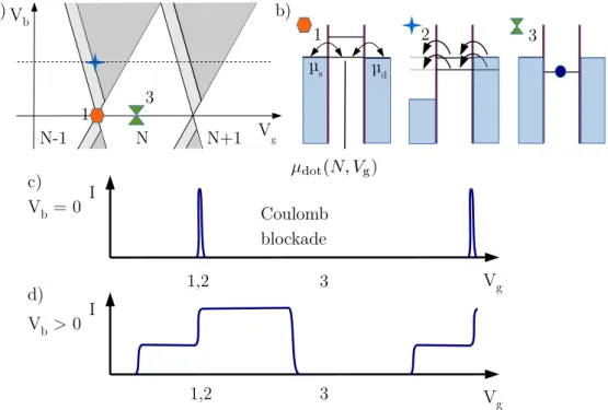
b). A typical result of such a measurement is sketched in Fig. 1.2(a).
The electro-chemical potential of the quantum dot is the minimum energy for adding the N th electron to the dot, i.e., µ
dot(N ) = U (N ) − U (N − 1), where U (N ) is the total ground state energy for N electrons on the dot at zero temperature [29]. Under the assumptions given above, namely that the electron-electron interaction between electrons on the dot and in the reservoirs can be modeled capacitively and under the additional assumption that these capacitances are independent of N , the electro-chemical potential of the quantum dot reads [29]
µ
dot(N, V
g) = ε
N+ e
2C
Σ(N + 1/2) − αeV
g, (1.2) where the capacitive influence of the gate reservoir is incorporated in α =
CCgΣ
.
Quantum dot spectroscopy 19
V
bV
g1
2 3
1 2 3
I
1,2 3 V
gCoulomb blockade
a) b)
c)
µ
sµ
dN-1 N N+1
I
1,2 V
gd) V
b= 0
V
b> 0
3
Figure 1.2: A short review on transport spectroscopy in the Coulomb blockade regime. (a) Schematic drawing of a current measurement as a function of gate and bias voltage. In the white region, the current is blocked and the number of electrons (given below the x-axis) is constant. (b) Electro- chemical potentials for three specific value-pairs of bias and gate voltage highlighted in (a). In 1, transport takes place through the ground state while in 2, a transition through an excited state contributes to the current. In 3, the current is blocked and the electron number on the dot is fixed to N . (c) Current plotted as a function of gate voltage at zero bias. When the
potentials of the dot and of the leads are aligned a peak is visible in the
current signal. (d) At finite bias, we observe steps when additional states
contribute to the transport.
In Eq. (1.2), the first term is the chemical potential, µ
ch= ε
N, while the other terms belong to the electrostatic potential eφ
N. The addition energy, i.e., the energy difference between two charging states with N and N + 1 electrons is given by
∆µ
N= µ
dot(N ) − µ
dot(N − 1) = ε
0+ e
2C
Σ, (1.3)
where we replaced the difference between the single particle energy states by a constant, ε
N− ε
N−1= ε
0. Note that we thereby assume that the single particle energies increase linearly with N .
At low bias and low temperature, i.e., eV
b, k
BT E
c, the condition for electron transport reads µ
s= µ
dot(N ) = µ
d. This situation is shown in Fig. 1.2(b) and marked by a hexagon in the stability diagram in Fig. 1.2(a).
Sweeping the gate voltage we thus expect a series of peaks in the current signal, separated by regions of the size ∆µ
N/α, where the tunneling is blocked by the Coulomb repulsion, see Fig. 1.2(c).
At finite bias, the situation is slightly different. The electro-chemical potential of the quantum dot with N electrons is modified by the capacitance to the reservoirs, i.e.,
µ
dot(N, V
g, V
b) = ε
N+ e
2C
Σ(N + 1/2) + e(α
sV
b− αV
g) (1.4) where α
s= C
s/(C
s+ C
d) describes the capacitive influence of the source reservoir on the quantum dot in relation to the drain reservoir [30].
At eV
b> k
BT, min(Γ
j), the condition µ
s≤ µ
dot≤ µ
dand µ
d> E
didefines a range of V
gvalues where tunneling from drain to source is possible.
Sweeping the gate voltage we observe steps in the current signal, Fig. 1.2(d), and, consequently, peaks in the conductance signal (not shown). Note that electrons can also tunnel through states of higher energy, e.g., the next state with µ
∗dot(N ) = µ
dot(N ) + ε
0, if the bias window is large enough. Such a situation is highlighted by a blue star in Fig. 1.2(a) and depicted in the second level scheme in (b). If the conditions µ
s< µ
∗dot(N ) and µ
d> µ
∗dot(N ) is met, the excited state contributes to the transport and we observe an additional step in the current Fig. 1.2(d) and a line in G = dI/dV
b(not shown).
In Fig. 1.2(c), the finite width of the peaks is determined by the tempera-
ture of the Fermi liquid in the lead reservoirs, compare Eq. (1.1). From this
consideration the condition E
ck
BT arises naturally as a requirement to
observe a Coulomb blockade signature similar to the one sketched in (c).
A carbon nanotube quantum dot 21
1.2 A carbon nanotube quantum dot
To this point, we did not touch the specific nature of the quantum dot. We assumed that the dot is a region that is confined in all spatial dimensions and this confinement determines the allowed electronic states by imposing boundary conditions on the solutions to the Schrödinger equation, Ψ
n(~k, ~r).
This implies a quantization of the wavevector ~k and a discretization of the energy spectrum. The relation between electron energy and wave vector on the quantum dot is given by the potential landscape that is set by the molecular arrangement of the quantum dot material.
In our case, the quantum dot under consideration is made up by a section of a carbon nanotube. The electron wavefunction forms a standing wave similar to the free particle-in-the-box textbook case, see Fig. 1.3. However, due to the particular nature of the graphene lattice, the relation between the wave vector and the quantization energy is linear in carbon nanotubes
2and, hence, such is the relation between the quantization energy and the tube length. We can understand most of the properties of a nanotube by considering the properties of a graphene sheet and taking into account the additional boundary conditions that are imposed by wrapping the sheet. This approach is termed the “zone-folding approximation” [31].
1.2.1 The graphene dispersion relation
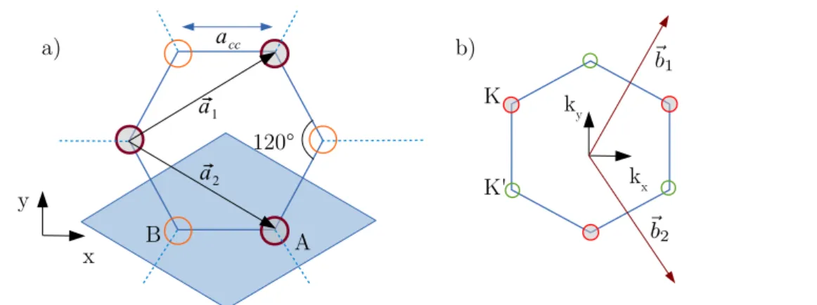
Graphene is an atomically thin layer of graphite. Its peculiar electronic properties arise from the perfect honeycomb lattice that is formed by the carbon atoms. The sp
2-hypridized orbitals of the carbon atoms form σ-bonds at 120
◦angles in the plane, see Fig. 1.4(a). The unit cell is spanned by two vectors
~a
1=
√ 3a 2 , a
2
!
and ~a
2=
√ 3a 2 , − a
2
!
,
and contains two atoms attributed to sublattices A and B. The lattice constant (common to both lattices) is given by
a = |~a
1| = |~a
2| = a
cc√
3 = 2.46Å,
where a
cc= 1.42 Å is the inter atomic distance of the carbon atoms, see Fig. 1.4(a). Correspondingly, the reciprocal lattice can be constructed with two symmetry points K ~ and K ~
0(also called Dirac points) in the first Brouillon
2
The CNT dispersion is approximately linear for states with energies ε . 1 eV.
Position along tube axis (nm)
0.0 1.0 2.0
0.1
0.0
-1.0
bi as v ol ta ge ( V )
Figure 1.3: Conductance from an STM tip to a CNT as a function of the position along the CNT and the applied bias voltage, adapted from Ref. [32].
The modulation of the conductance is interpreted as a modulation of the electron wavefunction in the CNT quantum dot where it forms a standing wave with a wavelength close to λ
F= 0.74 nm, the Fermi wavelength in carbon nanotubes.
x y
B A
120°
a ⃗
1a ⃗
2a) a
ccK
K' k
xk
yb)
Figure 1.4: (a) A segment of the graphene lattice. The small circles represent
carbon atoms, the lines between them represent σ-bonds. Note that the
graphene sheet can be built from two identical sublattices A and B with
common unit lattice vectors ~a
1and ~a
2. The blue shaded region highlights a
unit cell of the graphene lattice. (b) The first Brouillon zone of the graphene
lattice with lattice vectors ~b
1and ~b
2. Corresponding to the sublattices A and
B we find points K ~ and K ~
0in the reciprocal space.
A carbon nanotube quantum dot 23
zone,
K ~ = − 2π 3a , 2π
3 √ 3a
!
and K ~
0= − 2π
3a , − 2π 3 √
3a
!
. (1.5) We denote the length of these vectors by | K| ~ = | K ~
0| = 4π/3 √
3a ≡ K. The unit cell in the reciprocal lattice is spanned by unit vectors
~b
1= 2π
√ 3a , 2π a
!
and ~b
2= 2π
√ 3a , − 2π a
!
. (1.6)
The overlapping wave functions of the sp
2-hybridized electrons in the bonds form bands σ and σ
∗away from the Fermi energy which do not contribute to electronic transport. The remaining p
zorbitals are oriented perpendicular to the honeycomb lattice and constitute bonding π and anti-bonding π
∗bands. Electrons within these bands can move freely across the lattice and are responsible for the ballistic electron transport observed in graphene [33].
The dispersion relation of the valence (π
∗) and conduction (π) bands can be calculated by a tight-binding approach considering states on a graphene lattice with nearest neighbor overlap [34]. The dispersion relation reads [31]
ε
2D±(~k) = ±t
v u u
t 1 + 4 cos
√ 3k
xa 2
!
cos k
ya 2
!
+ 4 cos
2k
ya 2
!
, (1.7) where the plus sign applies to the π
∗and the minus sign to the π band, and the overlap energy is t = 2.6 ± 0.1 eV [31]. The energy surface defined by this relation is plotted in Fig. 1.5 for t = 2.7 eV. In the vicinity of the K ~ and K ~
0points the dispersion can be linearized. For a wave vector ~ q = ~k − K, with ~
~
q ~k
F, we obtain
ε
2D±(~ q) ≈ ±v
F|~ q| + O[(|~ q|/K)
2], (1.8) a linear function of |~ q| resembling the energy-momentum relation of a massless particle as a solution of the Dirac equation (~ q is measured from the Dirac points). From Eq. (1.7) it follows that v
F= √
3at/2 ≈ 8·10
5m/s for t = 2.5 eV.
In Fig. 1.5, a zoom-in shows one of the Dirac cones, i.e., the linear dispersion relation in the direct vicinity of a Dirac point.
1.2.2 The carbon nanotube dispersion relation
Conventionally, the structure of the rolled graphene sheet that forms a carbon
nanotube is characterized by its vector around the circumference in the basis
Figure 1.5: The electronic dispersion relation in graphene plotted as a surface in ~k-space. Clearly visible are the touching points between conductance and valence bands, the Dirac points. A zoom to one of these points highlights the linear evolution of the particle energy with the absolute value of ~ q in the vicinity of the Dirac points. Adapted from Ref. [35].
of the graphene lattice vectors ~a
1and ~a
2, i.e., C ~ = n~a
1+ m~a
2= (n, m). This vector forms an angle θ with the vector ~a
1,
cos(θ) = C ~ · ~a
1| C||~a ~
1| = 2n + m 2 √
n
2+ m
2+ nm , (1.9) where the hexagonal lattice symmetry restricts the chiral angle θ to 0
◦≤ θ ≤ 30
◦and the values of m to 0 ≤ m ≤ n. The diameter of a CNT is d = | C|/π. ~ In Fig. 1.6(A), examples are given for possible wrappings of the graphene sheet that form carbon nanotubes with C ~ = (11, 0) and C ~ = (11, 7). The atomic structure of the latter is shown in the STM image in Fig. 1.6(B). The special cases m = 0 and m = n are named according to the shape of the graphene “edge” along the vector C. Nanotubes where m = 0 are classified as zig-zag nanotubes while CNTs with m = n belong to the armchair class. The vast majority of possible geometries that do not fall into these two categories are called chiral tubes [31]. The smallest lattice vector T ~ perpendicular to C ~ determines the translational period t = | T ~ | of the tube. In the basis of the graphene lattice vectors, T ~ = t
1~a
1+ t
2~a
2, the components read
t
1= 2m + n
gcd(2m + n, 2n + m) and t
2= − 2n + m
gcd(2m + n, 2n + m ,
A carbon nanotube quantum dot 25
Figure 1.6: (A) Characterization of the carbon nanotube geometry. A
nanotube is formally constructed by rolling a graphene sheet along the vector
C. The translational vector ~ T ~ points along the tube axis. The angle between
C ~ and ~a
1is denoted by the chiral angle θ. A CNT with θ = 0
◦is called a
zigzag CNT, a CNT with θ = 30
◦is called an armchair CNT. (B) Atomically
resolved STM images of a armchair-like CNT with a chiral angle of θ = 27
◦and a diameter of d = 1.3 nm, corresponding to the (11, 7) nanotube whose
chiral vector is shown in (A). Adapted from Ref. [36].
where gcd(n
1, n
2) is the greatest common divisor of n
1and n
2. C ~ and T ~ span the translational unit cell of the CNT. We can also define a CNT unit cell using elementary helical chains. From the helical model, the distinction between different bands due to their crystal angular momentum m arises naturally. Please refer to Ref. [37] for a presentation of the helical model.
The most prominent effect of the wrapping on the dispersion relation E
±gof graphene is the restriction of the wave vector perpendicular to the nanotube axis to values spaced by ∆k
⊥= 2π/| C|. The quantum mechanical ~ confinement energy due to the radial confinement is of the order of eV (e.g., 1.1 eV for the nanotube in Fig. 1.6), so the dispersion relation is effectively restricted to the lowest subband in the bias and gate voltage ranges of the experiments presented in this work. Within a first approximation, we can deduce the carbon nanotube dispersion from the graphene dispersion by restricting the values of the wave vector to the one-dimensional subbands, i.e.,
ε(k
||, µ) = ε
2D±
k
||K ~
2| K ~
2| + µ ~ K
1
, (1.10)
where µ = 1, 2, . . . , N is an integer counting the subbands up to the number of carbon atom pairs in the translational unit cell N and
K ~
1= −t
2~b
1+ t
1~b
2N and K ~
2= m~b
1− n~b
2N .
From Eq. (1.10) we can distinguish metallic and semi-conducting nanotubes.
If for some µ the vector k
|| K~2|K~2|
+ µ ~ K
1is equal to K ~ or K ~
0, the valence band touches the conduction band and the tube is metallic, otherwise it is semi-conducting. It is straightforward to derive the condition for a metallic nanotube using Eq. (1.5),
n − m = 3q, where q is an integer number [38].
Classification of CNTs in terms of crystal angular momentum
We can further subdivide the large number of different chiral CNT geometries
by the crystal angular momentum quantum number m of the electrons in
the lowest lying one-dimensional subbands, i.e., the bands crossing the Dirac
point in the ~k-plane. Note that the assignment of m to a band is possible only
in the helical picture [39]. The crystal angular momentum in the armchair-
like class CNTs in these bands is always zero which can be expressed by
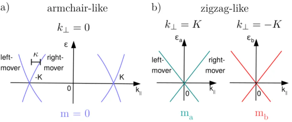
A carbon nanotube quantum dot 27
0 0
εa εb
k|| k||
m
am
bleft- mover
right- mover
b) zigzag-like
-K K
0 ε
k||
armchair-like a)
m = 0
left- mover
right- mover
Figure 1.7: Dispersion of the lowest lying band(s) in metallic CNTs. (a) In armchair-like CNTs, all states on the lowest lying conduction band share the same angular momentum, m = 0. The wave vector component perpendicular to the CNT axis is proportional to the angular momentum, k
⊥= 0. The branch to the left of the K ~ or K ~
0point in each valley is denoted the left-mover branch, the right branch is denoted the right-mover branch. The distance to the closest Dirac point is measured by κ. (b) zigzag-like CNTs host states with different angular momenta in the vicinity of the two Dirac points. Here, k
⊥= ±K in the two valleys, respectively.
the relation (n − m)/n|
mod 3= 0, where n = gcd(n, m) [37], see Fig. 1.7(a).
Note that metallic armchair tubes with n = m are a special case within this class. All other metallic tubes have non-zero angular momentum m
a= (2n + m)/3|
modnand m
b= (2m + n)3
modnin the bands crossing the K ~ and K ~
0points, respectively [39]. Since the angular momentum is defined mod n, we can always choose m
aand m
bwith m
a= −m
bwhich is required by time- reversal symmetry. The CNTs with different angular momentum for the states in the two valleys fall into the zigzag-like class, see Fig. 1.7(b). Again, zigzag CNTs with m = 0 are a special case within this class. In terms of the indices (n, m) we can distinguish armchair-like (and armchair) CNTs that satisfy (n − m)/n|
mod3= 0, and zigzag-like (and zigzag) CNTs where (n − m)/n|
mod36= 0.
In the CNT dispersion relation ε(k), see Fig. 1.7, we distinguish between
right- and left-moving branches for states with positive and negative wave
vectors measured from the Dirac point, respectively. In zigzag and zigzag-like
CNTs, the distance is measured by k with the corresponding sign and in
armchair and armchair-like CNTs the distance is measured by κ.
CNT curvature
This straightforward analysis neglects effects due to the curvature of the nanotube. From tight-binding calculations it can be seen that the nonzero curvature causes a shift in the ~k-plane [34]. More specifically, the allowed values of k
⊥are shifted such that a finite gap opens in all nominally metallic CNTs except armchair CNTs. The size of the gap is given by [40]
E
gap= 3ta
2cc16R
2cos(3θ) = ξ
R
2cos(3θ), (1.11)
where R = d/2 is the nanotube radius and ξ ' 1 eV/Å
2can be used to estimate the size of the bandgap for a tight-binding hopping parameter t = 2.6 eV [40]. According to Eq. (1.11), values for the size of the bandgap range from zero for armchair CNTs to 60 meV for (10, 0) zigzag CNTs.
3. Note, however, that typical single-wall CNTs have radii above 10 Å [42]. The model agrees with experimental observations [43]. More recently, larger bandgaps, up to 200 meV for the (10, 0) CNT are predicted within a non-orthogonal tight-binding model [44].
1.2.3 The single electron transport spectrum of a car- bon nanotube quantum dot
When we want to observe quantum Coulomb blockade in a carbon nanotube quantum dot, we have to provide a lateral confinement such that the condi- tions in Tab. 1.1 are satisfied. In the CNT transport setup, a confinement of the quantum dot is naturally given by the metallic leads which act as electrochemical potential barriers. However, we still have to take care to satisfy ~ Γ < k
BT . Depending on the material of the contacts and other fabrication parameters, it turns out that the tunnel coupling between the CNT and the leads can be too strong to observe Coulomb blockade [21].
These systems are better described in terms of ballistic electron wave-guides;
a subject that we discuss in the second part of this work.
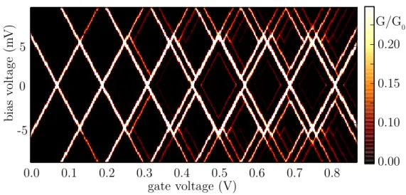
But not only the coupling between the nanotube and the electrode material is crucial. The coupling of the Fermi liquid reservoirs in the leads to the quantum dot on the carbon nanotube section between the contacts heavily depends on the electronic band structure that is modified by the gating potential. In Fig. 1.8 we plot current as a function of backgate voltage for a CNT suspended between two Rhenium contacts at a distance of 700 nm at T = 300 mK. We can clearly observe distinct Coulomb blockade peaks for
3
R ' 4 Å for a (10, 0) CNT, CNTs with R < 4 Å are not considered stable [41].
A carbon nanotube quantum dot 29
-4 gate voltage (V) 0 2 4
0.0 0.5 1.0 1.5 2.0
cu rr en t (1 0
-8A )
valence band band gap conduction band
Figure 1.8: Current plotted as a function of gate voltage (gatetrace) for sample CB3224 recorded at T = 300 mK and V
b= 50 µV. On the left, for values V
g< 0.5 V, we observe high currents and no Coulomb blockade. In this regime, no p-n-junction separates the quantum dot from the leads, as displayed by a schematic drawing in the left bottom corner. In the band-gap, no current can flow because the potential of the leads lies between valence and conduction band. On the right, for V
g> 1.5 V, distinct peaks are a clear signature for Coulomb blockade behavior. The transmittance of the interfaces is decreased by a p-n-junction induced by the highly deformed bands on both sides of the quantum dot.
positive values of the gate voltage beyond the band gap. In this region, a p-n-junction separates the leads from the quantum dot, creating an effective tunnel barrier with high opacity. For higher values of the gate voltage, the effective barrier width decreases and the Coulomb blockade peaks are broadened. For hole conduction through the valence band on the side with negative gate voltage, we observe high current values without a signature of Coulomb blockade.
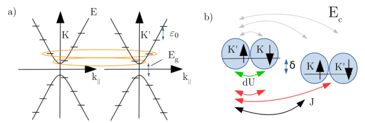
The lateral confinement due to the contacts or the p-n-junctions restricts the available k
||-bands, i.e., the continuous bands introduced in the previous section, to discrete levels, see Fig. 1.9(a), in the following called shells. In the fully degenerate case, a single shell can host up to four electrons with equal energy but different spin or ~k vector. In CNTs of the zigzag class, the states in the vicinity of the two Dirac points K ~ and K ~
0are distinguished by the
“valley” quantum number τ = ±1.
Kramers pairs At this point, all states in one shell are degenerate in energy,
occupying the lowest lying states on the two Dirac cones in the vicinity of
the K ~ and K ~
0points. When the time-reversal symmetry of the system is not
broken, e.g., by a magnetic field, each state can be transformed into one of
a) b)
K K'
k
||E
E
gk
||δ
E c
K' K
K K'
dU
J
Figure 1.9: The quantum dot spectrum in the constant interaction model.
(a) The dispersion relation of a carbon-nanotube with lifted degeneracy of the two Kramers pairs, due to, e.g., spin-orbit coupling. The longitudinal confinement imposes a restriction to discrete values of k
||. (b) Interaction of one electron (on the left) with the other electrons on the quantum dot on a mean-field level in the Oreg model. Thereby, J denotes the spin exchange interaction which has a different sign for parallel (black arrow) and anti- parallel spin (red arrows). dU denotes the interaction between electrons in the same spin-degenerate state (green arrow) and E
cis related to the inter-electronic Coulomb repulsion (grey arrows).
the other states by applying the time-reversal operation. The time-reversal operation flips the spin and the valley quantum numbers and thereby maps a state on its Kramers partner. Thus, the Kramers pairs in one CNT shell are given by |K, ↑i|K
0, ↓i and |K, ↓i|K
0, ↑i.
Analysis in terms of the constant interaction model
A first analysis of traces obtained at low bias voltage by varying the gate potential (e.g., the data shown in Fig. 1.8) can be done in terms of a mean field description of the interaction on the quantum dot [45].
We are interested in the addition energy spectrum, i.e., the spectrum of energies ∆µ
N= µ(N ) − µ(N − 1) at zero bias. In Eq. (1.2) we included the charging energy to account for the Coulomb repulsion between the electrons.
In principle, a careful analysis of the multi-electron ground states even at a mean field level yields a multitude of parameters describing different interactions between the electrons on the CNT quantum dot, see Fig. 1.10(b).
These include, e.g., the excess interaction between two electrons with opposite spin within one Kramers pair, dU , or the spin exchange interaction J [46, 47].
In the following we neglect the parameters dU and J, which are usually small
compared to ε
0, see Ref. [48].
A carbon nanotube quantum dot 31
1.5 2.0 2.5
32 36 40 Δμ
N(meV) 44
gate voltage (V) 5
6 7
8 2
band gap
Figure 1.10: Addition energies as a function of gate voltage for the sample CB3224 extracted from the gatetrace in Fig. 1.8. The numbers close to the crosses denote the electron number on the dot. The second shell is highlighted. For this shell, the analysis in terms of the constant interaction model is performed.
The addition energies of the four electronic states in one shell n can then be written as [46, 47, 49]
∆µ
4n+1= E
c+ ε
0(1.12)
∆µ
4n+3= E
c+ δ (1.13)
∆µ
4(n+2)= ∆µ
4n+4= E
c, (1.14)
where δ denotes an energy shift between the two Kramers pairs, see Fig. 1.9(a).
This shift is introduced as a subband mismatch to fit experimental data, e.g., in Ref. [49]. More recent works strongly suggest that it can be identified with the spin-orbit coupling strength in CNTs [16]. From the gatetrace in Fig. 1.8 we can extract the addition energy spectrum and estimate the parameters.
4In Fig. 1.10 we plot the distance between two peaks in gate voltage, corrected by a gate conversion factor α = 0.46 for sample CB3224. The first point in the plot corresponds to the energy required to add the second electron to the quantum dot. The addition energy for the first electron can not be resolved due to the band gap. Let us now focus on electron numbers N = 5 to N = 8. From the addition energies we extract the parameters of Eq. (1.12 - 1.14). We obtain E
c= 34 meV, δ = 5 meV and ε
0= 11.5 meV. The value for ε
0corresponds to a lateral extension of the CNT quantum dot of 150 nm where we used L = π ~ v
F/ε
0[31]. Compared to the distance between the contacts (700 nm), L(ε
0) is considerably smaller. However, the lateral
4
The values of the difference in gate voltage to add one electron have to be multiplied
by the lever arm α = C
g/C
Σ.
quantum dot size can be reduced significantly by the p-n-junctions [50]. The value of the valley splitting δ is found to be rather large compared to previous observations [16]. Please note that this model is heavily simplified and the parameters of the constant interaction model can not be directly mapped to microscopic parameters of the CNT. From Fig. 1.10 it is evident that the addition energies and thus the parameters of the model are not equal for the five shells that are visible, contrarily to the model predictions.
Single particle state spectroscopy of the one-electron state
We focus on the quantum dot state with one electron on the dot. Thereby we are confident that the effects of electron-electron interaction are sub- leading and we can treat the system within a single-particle approach. As a spectroscopic tool we apply a magnetic field B
palong the nanotube axis. The field induces a magnetic flux through the tube cross-section which changes the component of the wavevector which is perpendicular to the CNT axis, k
⊥[51]. This shifts the energy of the (discrete) states labeled by spin σ and valley τ by
E
σ,τ(B) = 1
2 g
sµ
BB
pσ + g
orbµ
orbB
pτ.
Adjusting the gate voltage to a value close to the first Coulomb peak to the right of the band gap, we can map the resonances that correspond to excited states within a finite bias voltage window,
5see Fig. 1.11(a). When we tune the magnetic field, we trace out the evolution of the four possible single particle states in the first two shells, see Fig. 1.11(b).
We analyze the data
6in this low-field (B
||= 0 − 2 T) regime using a linearized Hamiltonian in the spin and valley basis, i.e., {|K ↑i, |K ↓i, |K
0↑i
5
The measurement was performed together with Daniel Schmid and published in his thesis, Ref. [52].
6
The modeling that is presented in this section was performed by M. Marganska from
the group of M. Grifoni. The results are published in Ref. [52]
A carbon nanotube quantum dot 33
0 6
0.66 0.68
-10 -5 0 5 10
gate voltage (V) dI/dV
(10
-6e
2/h) 3
9
5
1 dI/dV (10
-6e
2/h)
-1 0 1 2
0 4 8 12
bi as v ol ta ge ( m V )
B
||(T)
a) b)
ε
0Δ
KK'Δ
K↑
K'↑
K↓
K'↓
N = 1
Figure 1.11: (a) Conductance as a function of bias and gate voltages in the
vicinity of the first charging state (“diamond”). We can clearly observe the
four lines corresponding to the two Kramers pairs of the first longitudinal
quantization state (shell) and two Kramers pairs of the second shell. The
lines are pointing towards the first charging state on the right. (b) Evolution
of the Kramers pairs with an increasing magnetic field along the nanotube
axis. Within each shell, the Kramers pairs at zero magnetic field are split
by ∆ (cf. δ in the Oreg model). The degeneracy of the constituents of the
pairs is lifted with magnetic field as indicated by the labels on the right. The
excited state energy is denoted by ε
0. Note that K and K
0states show an
anti-crossing at V
g= ±0.2 V with an energy scale ∆
KK0. Colored lines present
a fit to Eq. (1.15).
,|K
0↓i}:
H
lin= 1
2 g
sµ
BB
||
1 0 0 0
0 −1 0 0
0 0 1 0
0 0 0 −1
+ 1 2
∆
SO0 ∆
KK00
0 −∆
SO0 ∆
KK0∆
KK00 −∆
SO0
0 ∆
KK00 ∆
SO
+ B
||g
orb
µ
porb0 0 0 0 µ
aporb0 0 0 0 −µ
aporb0
0 0 0 −µ
porb
+ a|B
|||
1 0 0 0 0 1 0 0 0 0 1 0 0 0 0 1
(1.15) We recognize the first and the third term as being the Zeeman and the Aharonov-Bohm type energy dependence. The magnetic moments associated with the Aharonov-Bohm interaction are different for the two Kramers pairs.
The moment µ
porbis associated to the pair |K ↑i, |K
0↓i and the moment µ
aporbto the pair |K
0↑i, |K ↓i. The second term in Eq. (1.15) contains the spin-orbit coupling ∆
SO, and ∆
KK0, a mixing amplitude between the K and K
0orbital. The former is a consequence of the nanotube geometry and can be obtained from a careful derivation of the full dispersion relation [53]. The latter can be attributed to disorder [54] or arise due to scattering at the ends of the nanotube in the armchair-like geometry class [37], while it is absent in the pure armchair CNTs where mode mixing is prohibited by the parity symmetry.
7The origin of the last term in Eq. (1.15), which is proportional to a and to the modulus of the field is not clear. At the time of this writing, a is a fitting parameter in the ongoing analysis of the one-electron spectrum . In Tab. 1.2 we show the parameters that correspond to the fit presented in Fig. 1.11(b) together with the parameters from the constant interaction model of the previous section. The two Kramers pairs are shifted apart by an energy ∆ = q ∆
2SO+ ∆
2KK0at zero magnetic field, see Fig. 1.11(b). ∆ can be compared to δ from the Oreg model. However, the two values deviate by one order of magnitude. Note that the shell spacing ε
0= 1.4 meV extracted from the fit to the one electron spectroscopy data corresponds to an effective dot extension of 1.2 µm, almost two times larger than the distance between the contacts. In the vicinity of the band-gap, however, the finite curvature of the band reduces the energy spacing between two allowed values of k
||.
7
This will be discussed in more detail in Ch. 3.
A carbon nanotube quantum dot 35
shell 1 shell 2 CI
µ
aporb0.89 meV/T 0.77 meV/T - µ
porb0.88 meV/T 0.69 meV/T -
a 0.17 meV/T 0.05 meV/T -
∆
SO0.48 meV 0.41 meV -
∆
KK00.28 meV 0.21 meV -
∆/δ 0.56 meV 0.46 meV 5 meV
ε
21.4 meV 11.5 meV
Table 1.2: Parameters of the linearized Hamiltonian, Eq. (1.15), for the
first two shells extracted from the one electron spectroscopy. The values are
compared to the previous analysis in terms of the constant interaction model.
Chapter 2
Modeling a CNT quantum dot coupled to ferromagnetic leads
The considerations presented in the previous chapter are based on the as- sumption that the recorded transport data is solely determined by the energy spectrum of the quantum dot and the interaction of the electrons. The trans- port problem is treated as a sequence of single electron tunneling events with rates Γ k
BT that are given by an effective, energy independent coupling between the CNT and the leads, and the temperature.
In the experimental data discussed in this section,
1we observe a broadening of the Coulomb blockade peaks that can not be attributed to temperature.
Further on, this broadening is sensitive to the magnetic properties of the contacts. To correctly interpret the data, we have to go beyond the sequential tunneling description and present a model where the coupling is still smaller, but of the order of the temperature, i.e., Γ ≤ k
BT . Approaching this regime we have to take into account charge fluctuations between the quantum dot and the leads. To this end, we apply a transport framework based on the Liouville-von-Neumann equation [55], incorporating the quantum mechanical nature of the problem and allowing us to go beyond the considerations of Sec. 1.1.
The Liouville-von-Neumann equation describes the time evolution of the density matrix of the quantum mechanical problem fully taking into account the system under consideration and its surroundings. In general, the system has less degrees of freedom than the environment and its time evolution can sometimes be calculated exactly when it is decoupled from the environment.
Within the framework of the reduced density matrix theory we can start with
1
The data has been recorded by Daniel Steininger and Andreas Prüfling from the
University of Regensburg.
the exact solution for the decoupled system and perturb it by the coupling to the environment in a controlled way. Thereby we arrive at the quantum master equation (QME), which, in principle, describes the full dynamics of the weakly coupled system, see Ref. [56] for a review. The transport properties of the system are readily calculated from the QME. We follow the lines of Ref. [57] and present the so-called “dressed second order” (DSO) framework.
Eventually we apply this framework to the problem of a carbon nanotube quantum dot coupled to ferromagnetic leads and compare the results to the experimental data. The results presented in this chapter have been published in Ref. [58].
Note that there are numerous other frameworks to approach this problem, e.g., the non-equilibrium Green’s function technique [17], the Wigner function method [59], the Kubo [60] and the Boltzmann equation approach [61] or the equation-of-motion technique [62]. An approach that reaches beyond the DSO with a different summation scheme is the “resonant tunneling approximation”(RTA) [63]. For a spinless single electron transistor the RTA exactly describes the density matrix and thus the current in the intermediate regime Γ ≤ k
BT . A comparison shows that the DSO predicts the same current as the RTA in this case and thus captures the relevant diagrammatic contributions [57]. For more complicated systems as is the CNT quantum dot the RTA is increasingly difficult to handle while the DSO can be applied to more complex systems straightforwardly.
2.1 Introduction to the reduced density ma- trix approach
In the following, we give a short introduction to the basic concepts of the reduced density matrix approach to quantum transport. The reader that is familiar with the construction of the quantum master equation for the reduced density matrix might as well skip the following section and continue with the introduction of the dressed second order approach in Sec. 2.2.
2.1.1 Statistical mixtures
The largest set of mutually commuting independent observables provides the maximum available information about a quantum mechanical system. A state Ψ specified solely by the eigenvalues of these observables is a pure state
Ψ = X
n
a
n|φ
ni.
Introduction to the reduced density matrix approach 39
The choice of the set of observables is not unique. When the state of the system is not known, i.e., one can not provide a pure state, it is convenient to describe the system in terms of multiple possible states
|Ψ
ni = X
m0
a
(n)m0|φ
m0i,
and define a density matrix ˆ ρ = X
n
W
n|Ψ
nihΨ
n|, (2.1)
where W
nare real positive numbers and P
nW
n= 1. In the basis {|φi} the density operator takes the form
ˆ ρ = X
nmm0
W
na
(n)m0a
(n)∗m|φ
m0ihφ
m|,
or equivalently, in terms of matrix components:
hφ
i| ρ ˆ |φ
ji = X
n
W
na
(n)ia
(n)∗j. (2.2) The significance of this operator can be understood by the observation that the probability of finding the system in the state |Ψ
ni is W
nand that of selecting a certain eigenvector in this state, say |φ
mi, is |a
(n)m|
2. The diagonal elements,
ˆ
ρ
mm= X
n
W
n|a
(n)m|
2,
denote thus the probability to find the system in the eigenstate |Ψ
mi, summed over all possible basis states of the system. Analogously, the probability to find the system in the arbitrary state |Ψi is given by
P (Ψ) = X
n